EP0127347B1 - Breitbandsignalkopplungskreis mit variabler Gleichspannungspegelverschiebung zwischen Ein- und Ausgang - Google Patents
Breitbandsignalkopplungskreis mit variabler Gleichspannungspegelverschiebung zwischen Ein- und Ausgang Download PDFInfo
- Publication number
- EP0127347B1 EP0127347B1 EP84302995A EP84302995A EP0127347B1 EP 0127347 B1 EP0127347 B1 EP 0127347B1 EP 84302995 A EP84302995 A EP 84302995A EP 84302995 A EP84302995 A EP 84302995A EP 0127347 B1 EP0127347 B1 EP 0127347B1
- Authority
- EP
- European Patent Office
- Prior art keywords
- input
- output
- signal
- inverting
- operational amplifier
- Prior art date
- Legal status (The legal status is an assumption and is not a legal conclusion. Google has not performed a legal analysis and makes no representation as to the accuracy of the status listed.)
- Expired
Links
Images
Classifications
-
- G—PHYSICS
- G01—MEASURING; TESTING
- G01R—MEASURING ELECTRIC VARIABLES; MEASURING MAGNETIC VARIABLES
- G01R15/00—Details of measuring arrangements of the types provided for in groups G01R17/00 - G01R29/00, G01R33/00 - G01R33/26 or G01R35/00
- G01R15/08—Circuits for altering the measuring range
Definitions
- the present invention relates generally to signal coupling circuits, and in particular to a wide band-width signal coupling circuit having a variable DC voltage-level shift from input to output.
- Electronic signal-processing circuits are typically grouped in stages which are coupled together in such a manner that each stage may perform its intended operation without influencing or being influenced by the remaining stages, and without degrading signal fidelity.
- a very commonly encountered problem in connecting these stages together is that at the appropriate points of connection the signals or logic levels may have quiescent or average values which are other than zero volts.
- a typical method of coupling circuit stages together is by coupling capacitors or transformers; however, these methods are not practical if DC information is to be preserved.
- Zener diodes or even batteries are sometimes used to provide a fixed DC level shift.
- these devices introduce an uncertain resistance value in series with the input signal path, resulting in difficulties in impedance matching.
- the inherent capacitance of these devices serves to limit the frequency bandwidth of signals being transmitted therethrough.
- ECL emitter-coupled logic
- the output is pulled down to a negative supply (usually about - 2 volts) with an external pull-down resistor (usually 50 to 100 ohms). Since speed is a major consideration in ECL designs the interconnections between logic gates are often transmission lines, and the pull-down resistor doubles as a line termination. If a conventional 500-ohm, 10 X passive probe were used in conjunction with an oscilloscope to examine an ECL output, the probe's 500-ohm resistance to ground would form a voltage divider with the output termination resistor of the particular logic gate being examined. This divider can cause severe distortion of the output signal level, shift the DC operating point of the output transistor of the logic gate, and greatly reduce the gate's noise margin.
- DE-A-2 810 951 discloses a circuit for coupling signals to the input of an electronic device, the circuit being arranged to eliminate DC components of the signals.
- the DC component is compensated using an impedance network consisting of 3 resistors connected in, eg., a ⁇ -style.
- the junction between the first and second resistors forms an input terminal and the junction between the second and the third resistors forms an output terminal.
- DC voltage sources are connected to the opposite ends of the first and third resistors. These sources cause the DC component to be compensated without giving rise to any currents that would affect the input signal.
- a capacitor is coupled in parallel between the input and output terminals, and the second voltage source is derived from the first voltage source using an inverting amplifier. Such an arrangement is not suitable for preserving DC information.
- a method of coupling components of a signal at an input terminal to an output terminal comprising coupling high frequency components of the signal using a high frequency signal transmission path comprising a capacitor coupled between said input terminal and said output terminal, characterised in that the DC component of the signal is coupled, together with the low frequency components of the signal, by means of an inverting operational amplifier having inverting and non-inverting inputs, a feedback path coupled between the output and inverting input of said operational amplifier, and an input resistor serially connected between the input terminal and said inverting input, and by means of a differential amplifier having an input connected to the output of said operational amplifier and an output connected to said output terminal and in that the DC offset at the output terminal is adjusted by altering the DC voltage at the non-inverting input of said operational amplifier.
- the invent also extends to a signal coupling circuit according to Claim 2 suitable for coupling signal components using such a method.
- a feature of the invention is that the values of impedance elements for both the high-frequency and low-frequency transmission paths may be selected to provide predetermined output and output impedances for impedance matching purposes without compromising signal fidelity or limiting the signal bandwidth.
- the signal coupling circuit of the present invention is suitable for a wide variety of applications, such as, for example, for 50-ohm systems, since the input impedance may be made equal to the load impedance at high frequencies.
- the preferred embodiment taught herein is implemented in a passive 10X attenuator probe having a 500-ohm input impedance, a 50-ohm output impedance, and a 1.5 gigahertz pass band. Even though a series impedance is required to effect the desired divide-by-ten signal reduction, because of the manner in which the DC level shift mechanism is implemented, the level shift voltage provided via the probe tip to the signal source is attenuated only slightly so that a wide range of variable level shift voltage (also known as DC offset) is provided without limiting circuit band-width.
- a high-speed probe including the preferred embodiment of the present invention is particularly suited to ECL and TTL logic systems.
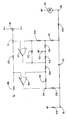
- the single FIGURE shows a detailed schematic diagram of a signal coupling circuit according to the preferred embodiment.
- a signal coupling circuit in which both a high-frequency signal transmission path and a low-frequency signal transmission path are coupled between an input terminal 10 and an output terminal 12.
- a voltage generator (e g ) 14 is shown connected to input terminal 10, and it should be understood that such voltage generator may suitably represent the output of another circuit and as such may be, for example, a test point to be connected to an oscilloscope for viewing. Accordingly, the quiescent (DC) or average voltage of voltage generator 14 may be other than zero volts; for example, it may be the lower -1.7-volt level of an ECL circuit.
- the high-frequency signal transmission path comprises a capacitor Cl.
- the low-frequency signal transmission path which is substantially in parallel with capacitor C1, comprises resistors R1, R2, R3, R4, R5, and R6.
- Resistors R2 and R4 are serially connected in the feedback path of an inverting operational amplifier, the active element of which is amplifier U1.
- Resistors R5 and R6, amplifier U2, and resistors R7 and R8 form a differential amplifier.
- Amplifiers U1 and U2 suitably may be commercially-available field-effect transistor (FET) input "op amps" with very high input impedance at the inverting (-) and non-inverting (+) inputs thereof.
- a load resistor R9 is shown connected between output terminal 12 and ground.
- a resistor R10 is connected from the junction of resistors R1 and R2 to the inverting input of op amp U1 to isolate the high-frequency loading represented by the high stray capacitance of the op amp input from the signal source.
- Resistor R10 should have a fairly large value, e.g., 10 kilohms or higher, so that the dominant loading of the lower end of resistor R1 is resistor R2. Accordingly, resistor R2 should have a comparatively small value, e.g., less than one kilohm, so that any loading represented by resistor R10 is substantially negligible.
- a capacitor C2 may be connected from the output of op amp U1 to the inverting input thereof to provide a maximum, but controlled step response for the low-frequency transmission path.
- the value of capacitance chosen depends upon the particular op amp type used, with op amp stability and control of the response speed being the design criteria.
- a capacitor C3 may be connected to ground from the junction of resistors R2 and R4 to form a phase-lead network which forces op amp U1 to compensate for the phase lag due to the finite bandwidth of op amp U2, delaying the current through resistor R1 by an amount equal to the phase-lag-caused delay of current in resistor R3.
- the current delivered through resistor R2 to output terminal 12 from the output of op amp U2 is phase delayed compared with the input signal simply due to the rolloff of higher-frequency response through the low-frequency signal transmission path.
- op amp U1 acts dynamically to maintain a "virtual ground" at the junction of resistors R1 and R2 by feeding back the required current to match the input signal current, capacitor C3 causes a delay just sufficient to allow the output of op amp U2 to respond.
- the net result is a smooth time changeover of the current into the R1-C1 node from capacitor C1 to resistor R1.
- resistors R2 and R4 may be replaced by a single feedback resistor.
- An optional series resistor R11 is included in the signal path between input terminal 10 and the junction of resistor R1 and capacitor C1 if the signal coupling circuit is to provide attenuation as well.
- a potentiometer 16 which is disposed between a pair of suitable voltage supplies +V and -V, produces a variable level-shift voltage V1 at a movable wiper arm thereof.
- the level shift voltage V1 is applied to the non-inverting input of op amp U1 and to one end of resistor R7. Since it is a characteristic of inverting operational amplifiers for the inverting input to actively balance the potential applied to the non-inverting input, the level-shift voltage is transmitted to the operational amplifier null point or "virtual ground" at the junction of resistors R1 and R2.
- the level-shift voltage is adjusted to match the quiescent (DC) or average voltage of the signal source represented by signal generator 14; when this match is achieved, no current flows through resistor R1, nor does any current flow through feedback resistors R2 and R4 in this condition.
- the level-shift voltage V1 is applied to the junction of resistors R4 and R5, matching the voltage V1 applied to resistor R7, and the output voltage V2 from the differential amplifier is zero volts, provided the resistance values of resistors R5, R6, R7, and R8 are properly selected.
- the ratios of values should be equal on the two sides of the amplifier to provide the symmetry required for common mode rejection.
- resistors R5 and R6 are equal in value so as to provide unity gain
- resistors R7 and R8 should be also be. In the preferred embodiment, all four resistors are the same value.
- level-shift voltage feature of the present invention is in connecting to an oscilloscope a signal having a quiescent DC voltage level other than zero volts.
- a passive signal acquisition probe containing the preferred embodiment is connected between the signal source and the oscilloscope input.
- the quiescent DC voltage level of the signal source if other than ground potential, causes the trace to jump away from screen center to a distance represented by the DC voltage.
- potentiometer 16 is then adjusted to bring the trace back to screen center; that is, a value of voltage V1 has been produced to match the DC level of the signal source so that voltage V2 at the output of op amp U2 is equal to zero volts.
- a proposed commercial embodiment is a passive 10X attenuator probe having a 500-ohm input, a 50-ohm output, and a l.5-gigahertz bandwidth.
- Resistors R11 and R1 have values of 450 ohms and 50 ohms, respectively, providing both the desired 500-ohm input impedance and the divide-by-ten signal division.
- the 50-ohm output impedance is provided by a 50-ohm coaxial cable connected between the junction of capacitor C1 and resistor R3 and the output terminal 12.
- the load resistor R9 may suitably be a 50-ohm resistor to terminate the coaxial transmission line.
- Resistors R5, R6, R7, and R8 are each 10-kilohm resistors, and resistor R3 is a one-kilohm resistor. It should be noted that resistor R3 appears in parallel with resistor R9 to signals passing through the high-frequency signal transmission path (capacitor C1), and thus should be chosen to be substantially larger than the load resistor. The effect of the resulting attenuation of the R3-R9 voltage divider ratio in the low-frequency signal transmission path may be cancelled by selecting the gain of the operational amplifier U1 (actually the ratio of resistors R1 and R2) to be equal to the attenuation, as long as the gain of the differential amplifier U2 is one.
- the overall gain of the low-frequency path including the level-shifting operational amplifier (op amp U1 and its associated circuit elements including the R3-R9 divider) and the output differential amplifier (op amp U2 and its associated circuit elements) is unity so that there is no signal loss.
- Capacitor C1 has a value of one microfarad.
- the values of R2, R4, R10, C2, and C3 are selected to set the proper gain and step response and to provide an overall frequency response that is substantially flat over the entire 1.5-gigahertz frequency range.
- the level shift provided by this embodiment is approximately + and - 5 volts.
Landscapes
- Physics & Mathematics (AREA)
- General Physics & Mathematics (AREA)
- Amplifiers (AREA)
- Logic Circuits (AREA)
Claims (3)
- Verfahren zum Ankoppeln einer Signalkomponente einer Eingangsanschlußklemme (10) an eine Ausgangsanschlußklemme (12), wobei das Verfahren aus dem Ankoppeln von Hochfrequenzkomponenten des Signals unter Verwendung eines Hochfrequenzsignalübertragungsweges besteht, der einen zwischen der Eingangsklemme (10) und der Ausgangsklemme (12) angekoppelten Kondensator (C1) aufweist,
dadurch gekennzeichnet, daß
die Gleichstromkomponente des Signals mit den Niedrigfrequenzkomponenten zusammen verkoppelt ist und zwar über einen umkehrenden Betriebsverstärker (U1) mit Umkehr- und Nichtumkehreingängen, einem zwischen den Ausgang und den umkehrenden Eingang des Betriebsverstärkers (U1) gekoppelten Rückkopplungsweg (R2, R4, C2, C3, R10) und einen Eingangswiderstand (R1), der zwischen der Eingangsanschlußklemme (10) und dem umkehrenden Eingang in Reihe verbunden ist und über einen Differentialverstärker (R5 - R8, U2) mit einem mit dem Ausgang des Betriebsverstärkers verbundenen Eingang und einem mit der Ausgangsklemme (12) verbundenen Eingang, und dadurch daß die Gleichstromaufprägung an der Ausgangsklemme durch Verändern der Gleichstromspannung an dem nichtumkehrenden Eingang des Betriebsverstärkers eingestellt wird. - Eine Signalkopplungsschaltung zum Verkoppeln von Signalkomponenten gemäß dem Verfahren von Anspruch 1, wobei das Signal aus:- einem Hochfrequenzsignalübertragungsweg mit einem zwischen der Eingangsklemme (10) und der Ausgangsklemme (12) angekoppelten Kondensator (C1)- einem Niederfrequenzübertragungsweg (R1 - R8, R10, C2, C3, U1, U2), welcher einen Umkehrbetriebsverstärker (U1) und einen zwischen der Eingangsklemme (10) und der Ausgangsklemme (12) in Reihe geschalteten Differentialverstärker (R5 bis R8, U2) aufweist, wobei der Betriebsverstärker (U1) umkehrende und nichtumkehrende Eingänge, einen zwischen den Ausgang und den umkehrenden Eingang des Betriebsverstärkers (U1) angeschlossenen Rückkopplungsweg (R2, R4, C2, C3, R10) und einen in Reihe zwischen die Eingangsklemme (10) der Verkopplungsschaltung und den umkehrenden Eingang des Betriebsverstärkers (U1) geschalteten Eingangswiderstand (R1) hat und- einer Spannungsquelle für veränderlichen Gleichstrom besteht, mit einem Potentiometer (16), der an dem nichtumkehrenden Eingang des Betriebsverstärkers (U1) angeschlossen ist.
- Eine Signalverkopplungsschaltung gemäß Anspruch 2, worin der Betriebsverstärker (U1) außerdem ein Phasen-Voreilungs-Impedanz-Netz (C3) in seinem Rückkopplungsweg für den Ausgleich einer Phasennacheilungs-Betriebscharakteristik des Differentialverstärkers (R5 bis R8, U2) aufweist.
Applications Claiming Priority (2)
| Application Number | Priority Date | Filing Date | Title |
|---|---|---|---|
| US06/497,917 US4551636A (en) | 1983-05-25 | 1983-05-25 | Wide bandwidth signal coupling circuit having a variable voltage-level shift from input to output |
| US497917 | 1983-05-25 |
Publications (3)
| Publication Number | Publication Date |
|---|---|
| EP0127347A2 EP0127347A2 (de) | 1984-12-05 |
| EP0127347A3 EP0127347A3 (en) | 1986-04-16 |
| EP0127347B1 true EP0127347B1 (de) | 1991-02-20 |
Family
ID=23978862
Family Applications (1)
| Application Number | Title | Priority Date | Filing Date |
|---|---|---|---|
| EP84302995A Expired EP0127347B1 (de) | 1983-05-25 | 1984-05-03 | Breitbandsignalkopplungskreis mit variabler Gleichspannungspegelverschiebung zwischen Ein- und Ausgang |
Country Status (5)
| Country | Link |
|---|---|
| US (1) | US4551636A (de) |
| EP (1) | EP0127347B1 (de) |
| JP (1) | JPS60132417A (de) |
| CA (1) | CA1215439A (de) |
| DE (1) | DE3484116D1 (de) |
Families Citing this family (16)
| Publication number | Priority date | Publication date | Assignee | Title |
|---|---|---|---|---|
| US4737735A (en) * | 1986-07-25 | 1988-04-12 | Kampes Donald P | Phantom powered amplifier |
| US4857825A (en) * | 1988-09-16 | 1989-08-15 | Datatape, Inc. | Voltage controlled resistor |
| GB9317075D0 (en) * | 1993-08-17 | 1993-09-29 | Blomley Peter F | An improved amplifier |
| US5539354A (en) * | 1993-08-18 | 1996-07-23 | Carsten; Bruce W. | Integrator for inductive current sensor |
| WO1996010865A1 (en) * | 1994-10-03 | 1996-04-11 | Motorola Inc. | Method and apparatus for providing a low voltage level shift |
| US6087881A (en) * | 1998-07-23 | 2000-07-11 | International Business Machines Corporation | Integrated circuit dual level shift predrive circuit |
| US7256575B2 (en) * | 2004-06-01 | 2007-08-14 | Tektronix, Inc. | Wide bandwidth attenuator input circuit for a measurement probe |
| JP4668599B2 (ja) * | 2004-12-14 | 2011-04-13 | 岩通計測株式会社 | 広帯域オフセット回路 |
| JP2007201864A (ja) * | 2006-01-27 | 2007-08-09 | Yokogawa Electric Corp | レベルシフト回路 |
| JP4910520B2 (ja) * | 2006-07-07 | 2012-04-04 | 横河電機株式会社 | アクティブプローブ |
| US8129867B2 (en) * | 2008-06-27 | 2012-03-06 | National Instruments Corporation | RF AC/DC coupling circuit using general purpose solid-state relay |
| US8022730B2 (en) * | 2009-10-13 | 2011-09-20 | Himax Technologies Limited | Driving circuit with slew-rate enhancement circuit |
| CN102053177B (zh) * | 2009-11-10 | 2014-12-10 | 北京普源精电科技有限公司 | 一种有源差分电压探头 |
| DE112017005338T5 (de) * | 2016-10-19 | 2019-07-11 | Microsemi Storage Solutions, Inc. | Virtuelles Hybrid zur Vollduplexübertragung |
| US10778089B2 (en) * | 2017-04-07 | 2020-09-15 | Texas Instruments Incorporated | Cascaded active electro-magnetic interference filter |
| US11601045B2 (en) | 2019-04-01 | 2023-03-07 | Texas Instruments Incorporated | Active electromagnetic interference filter with damping network |
Family Cites Families (7)
| Publication number | Priority date | Publication date | Assignee | Title |
|---|---|---|---|---|
| US3393369A (en) * | 1965-10-22 | 1968-07-16 | Electronic Associates | Feedback limiter circuit having voltage gain amplifier |
| FR2112727A5 (de) * | 1970-11-06 | 1972-06-23 | Sercel Rech Const Elect | |
| GB1390341A (en) * | 1971-03-12 | 1975-04-09 | Dolby Laboratories Inc | Signal compressors and expanders |
| US4011504A (en) * | 1975-06-12 | 1977-03-08 | Depillo Lawrence V | Solid state scale expanding circuit for electrical indicator devices |
| US4142110A (en) * | 1977-04-07 | 1979-02-27 | Fa. Weber Lichtsteuergerate Kg. | Circuit to eliminate DC bias |
| DE2810951C2 (de) * | 1978-03-14 | 1980-02-07 | Hewlett-Packard Gmbh, 7030 Boeblingen | Kompensationsschaltung für elektronische Meßgeräte |
| US4403183A (en) * | 1981-04-10 | 1983-09-06 | Tektronix, Inc. | Active voltage probe |
-
1983
- 1983-05-25 US US06/497,917 patent/US4551636A/en not_active Expired - Lifetime
-
1984
- 1984-05-03 EP EP84302995A patent/EP0127347B1/de not_active Expired
- 1984-05-03 DE DE8484302995T patent/DE3484116D1/de not_active Expired - Lifetime
- 1984-05-08 CA CA000453794A patent/CA1215439A/en not_active Expired
- 1984-05-25 JP JP59106340A patent/JPS60132417A/ja active Granted
Also Published As
| Publication number | Publication date |
|---|---|
| CA1215439A (en) | 1986-12-16 |
| JPH0510849B2 (de) | 1993-02-10 |
| DE3484116D1 (de) | 1991-03-28 |
| EP0127347A2 (de) | 1984-12-05 |
| US4551636A (en) | 1985-11-05 |
| EP0127347A3 (en) | 1986-04-16 |
| JPS60132417A (ja) | 1985-07-15 |
Similar Documents
| Publication | Publication Date | Title |
|---|---|---|
| EP0127347B1 (de) | Breitbandsignalkopplungskreis mit variabler Gleichspannungspegelverschiebung zwischen Ein- und Ausgang | |
| US5604463A (en) | Coupling circuit | |
| US7256575B2 (en) | Wide bandwidth attenuator input circuit for a measurement probe | |
| DE69232705T2 (de) | Hochgeschwindigkeitsbus-Sender-Empfänger mit fehlertoleranter Realisierung für on-line-steckbare Verwendungen | |
| US4491802A (en) | Wide-band amplifier system | |
| US4206416A (en) | Wideband instrumentation amplifier with high common mode rejection | |
| US2663766A (en) | Transistor amplifier with conjugate input and output circuits | |
| EP0114731A1 (de) | Differenzverstärker mit hoher Gleichtaktunterdrückung | |
| EP0494420B1 (de) | Stromsenke | |
| US4425551A (en) | Differential amplifier stage having bias compensating means | |
| DE19858078B4 (de) | Signalverstärkerschaltung mit symmetrischen Ein- und Ausgängen | |
| EP0420341B1 (de) | Gegentakt-Filterschaltung | |
| US4514704A (en) | Variable filter circuit | |
| DE3854617T2 (de) | Elektronischer hochgeschwindigkeitsschaltkreis in kaskodenkonfiguration. | |
| USRE23563E (en) | Control of impedance of semicon | |
| CA1252523A (en) | Level shift circuit for differential signals | |
| US5300893A (en) | Amplifier | |
| US5402084A (en) | Coupling circuit | |
| DE69011667T2 (de) | Modulatorschaltung. | |
| US5150074A (en) | Wide-band transconductance generator | |
| US4495458A (en) | Termination for high impedance attenuator | |
| US4845446A (en) | Dynamically variable attenuator | |
| US3980966A (en) | Circuit arrangement for the receiving of binary direct current signals which are transmitted with low transmission voltage over galvanically connected lines | |
| US7205833B2 (en) | Method and circuit for reduced setting time in an amplifier | |
| US11394376B2 (en) | Crosstalk cancellation circuit, transmitter, and transmission and reception system |
Legal Events
| Date | Code | Title | Description |
|---|---|---|---|
| PUAI | Public reference made under article 153(3) epc to a published international application that has entered the european phase |
Free format text: ORIGINAL CODE: 0009012 |
|
| AK | Designated contracting states |
Designated state(s): DE FR GB NL |
|
| PUAL | Search report despatched |
Free format text: ORIGINAL CODE: 0009013 |
|
| AK | Designated contracting states |
Kind code of ref document: A3 Designated state(s): DE FR GB NL |
|
| 17P | Request for examination filed |
Effective date: 19860728 |
|
| 17Q | First examination report despatched |
Effective date: 19880324 |
|
| RAP1 | Party data changed (applicant data changed or rights of an application transferred) |
Owner name: TEKTRONIX, INC. |
|
| GRAA | (expected) grant |
Free format text: ORIGINAL CODE: 0009210 |
|
| AK | Designated contracting states |
Kind code of ref document: B1 Designated state(s): DE FR GB NL |
|
| ET | Fr: translation filed | ||
| REF | Corresponds to: |
Ref document number: 3484116 Country of ref document: DE Date of ref document: 19910328 |
|
| PLBE | No opposition filed within time limit |
Free format text: ORIGINAL CODE: 0009261 |
|
| STAA | Information on the status of an ep patent application or granted ep patent |
Free format text: STATUS: NO OPPOSITION FILED WITHIN TIME LIMIT |
|
| 26N | No opposition filed | ||
| PGFP | Annual fee paid to national office [announced via postgrant information from national office to epo] |
Ref country code: FR Payment date: 19920408 Year of fee payment: 9 |
|
| PGFP | Annual fee paid to national office [announced via postgrant information from national office to epo] |
Ref country code: NL Payment date: 19920531 Year of fee payment: 9 |
|
| PG25 | Lapsed in a contracting state [announced via postgrant information from national office to epo] |
Ref country code: NL Effective date: 19931201 |
|
| NLV4 | Nl: lapsed or anulled due to non-payment of the annual fee | ||
| PG25 | Lapsed in a contracting state [announced via postgrant information from national office to epo] |
Ref country code: FR Effective date: 19940131 |
|
| REG | Reference to a national code |
Ref country code: FR Ref legal event code: ST |
|
| REG | Reference to a national code |
Ref country code: GB Ref legal event code: IF02 |
|
| PGFP | Annual fee paid to national office [announced via postgrant information from national office to epo] |
Ref country code: GB Payment date: 20030417 Year of fee payment: 20 |
|
| PGFP | Annual fee paid to national office [announced via postgrant information from national office to epo] |
Ref country code: DE Payment date: 20030428 Year of fee payment: 20 |
|
| PG25 | Lapsed in a contracting state [announced via postgrant information from national office to epo] |
Ref country code: GB Free format text: LAPSE BECAUSE OF EXPIRATION OF PROTECTION Effective date: 20040502 |
|
| REG | Reference to a national code |
Ref country code: GB Ref legal event code: PE20 |