EP0125608B1 - Single longitudinal mode semiconductor laser - Google Patents
Single longitudinal mode semiconductor laser Download PDFInfo
- Publication number
- EP0125608B1 EP0125608B1 EP84105167A EP84105167A EP0125608B1 EP 0125608 B1 EP0125608 B1 EP 0125608B1 EP 84105167 A EP84105167 A EP 84105167A EP 84105167 A EP84105167 A EP 84105167A EP 0125608 B1 EP0125608 B1 EP 0125608B1
- Authority
- EP
- European Patent Office
- Prior art keywords
- optical waveguide
- layer
- bragg reflector
- distributed bragg
- semiconductor laser
- Prior art date
- Legal status (The legal status is an assumption and is not a legal conclusion. Google has not performed a legal analysis and makes no representation as to the accuracy of the status listed.)
- Expired
Links
Images


Classifications
-
- H—ELECTRICITY
- H01—ELECTRIC ELEMENTS
- H01S—DEVICES USING THE PROCESS OF LIGHT AMPLIFICATION BY STIMULATED EMISSION OF RADIATION [LASER] TO AMPLIFY OR GENERATE LIGHT; DEVICES USING STIMULATED EMISSION OF ELECTROMAGNETIC RADIATION IN WAVE RANGES OTHER THAN OPTICAL
- H01S5/00—Semiconductor lasers
- H01S5/10—Construction or shape of the optical resonator, e.g. extended or external cavity, coupled cavities, bent-guide, varying width, thickness or composition of the active region
- H01S5/12—Construction or shape of the optical resonator, e.g. extended or external cavity, coupled cavities, bent-guide, varying width, thickness or composition of the active region the resonator having a periodic structure, e.g. in distributed feedback [DFB] lasers
- H01S5/125—Distributed Bragg reflector [DBR] lasers
Definitions
- the present invention relates to a single longitudinal mode semiconductor laser suitable as a light source for optical fiber communication systems.
- the transmission loss of optical fibers has been so drastically reduced as to be no more than 0.2 to 0.5 dB/km in the 1.3 and 1.5 micron wavelength bands, it has become possible to realize an optical fiber communication system having a relaying distance of more than 100 km.
- the transmissible relaying distance and capacity are limited not only by the transmission loss of optical fibers but also by wavelength dispersion.
- the effect of wavelength dispersion is remarkable in long-distance optical fiber transmission using the conventional Fabry Perot resonator type semiconductor lasers, which usually has a plurality of oscillating longitudinal modes. Therefore, realization of a long-distance large-capacity optical fiber communication system would require semiconductor lasers capable of oscillating in a single longitudinal mode even in high-speed modulation.
- Such semiconductor lasers include the distributed feedback laser diode (DFB LD) with a built-in diffraction grating having a periodic structure and the distributed Bragg reflector laser diode DBR LD).
- DBR LD distributed feedback laser diode
- These semiconductor lasers which can select the oscillation longitudinal mode, are still in the process of research and development, and only recently became capable of continuous operation at room temperature. There is a long way to go before they can be successfully applied to practical purposes because they are inferior to the conventional Fabry Perot oscillator type semiconductor laser in such basic performance features as oscillation threshold and differential quantum efficiency. The biggest reason for their inferiority consists in their lower equivalent reflecting power, which in turn results from the weak coupling between light and the periodic structure constituting the diffraction grating, resulting in a poor light diffraction efficiency.
- a 'DBR LD for instance, a low reflecting power in the diffraction grating section invites an increase in injection current required for laser oscillation.
- the region in which the grating is formed has to be made as long as possible in order to increase the reflecting power in the diffraction grating section, the overall element length in inevitably extended to around 1 mm, and there are a number of other disadvantages in element performance and fabrication aspects.
- a semiconductor laser diode in accordance with the present invention, comprises a distributed Bragg reflector formed on a substrate.
- the reflector includes an optical waveguide sandwiched between first and second cladding regions and formed over the substrate, the optical waveguide having a corrugated region extending within the optical waveguide in a direction parallel to the surface of the substrate.
- the thickness of the corrugated region varies in a prescribed period and the refractive index of the corrugated region differs from that of the optical waveguide.
- An optically active layer formed over the substrate is butt-joined to the optical waveguide, and emits light beams when a current is injected into it.
- Fig. 1 shows a sectional view of a diffraction grating constituting a distributed Bragg reflector of prior art structure, so composed that semiconductor layers 1 and 3 having refractive indices n 1 and n 3 , respectively, sandwich between them a semiconductor optical waveguide layer 2 having a refractive index n 2 , which is greater than both n 1 and n 3 - Over the top of the optical waveguide layer 2 there is formed periodic structure having a period ⁇ and a depth d.
- a light beam entering the optical waveguide 2 of the distributed Bragg reflector in the direction of the z axis from the lefthand side of the figure propagates confined within this optical waveguide layer 2 because the refractive index n 2 of this layer 2 is greater than those of the upper and lower layers.
- the effective refractive index n 2 of the layer 2 also periodically varies in the direction of the z axis.
- the maximum value of the reflecting power R B in this waveguide is given by the following equation: where K is the coupling constant of corrugation and L, the length of the waveguide. Because the reflecting power R e , max rises with increases in K and L, performance improvements including reduction of the oscillation threshold of the semiconductor laser can be thereby achieved. However, merely increasing L while keeping K small would invite an increase of loss owing to the absorption of light during propagation through the optical waveguide 2 among other reasons. Therefore, the enlargement of K is vital to improving the performance features of the semiconductor laser. K is given by the following equation: where S y(x) is the electric field distribution of light beams in the y direction and Aii(x) is the variation of the effective refractive index.
- Fig. 2 shows a sectional view of a distributed Bragg reflector to be used in the present invention.
- n 4 refractive index
- the electric field component of light beams subjected to the periodic variations of the refractive index, as illustrated by the electric field distribution of light beams in Fig. 2 can be maximized, so that the value of K can be increased.
- the magnitude of the electric field of light beams in the central section of the optical waveguide layer 2 is from three to ten times greater than that of the electric field of light beams on the upper or lower face of the same. Accordingly, the structure of Fig. 2 can result in a K value 10 to 100 times greater than that of Fig. 1.
- K can be made evidently larger than in the structure of Fig. 1. Therefore, the reflecting power R B can be enlarged, resulting in a remarkable improvement of the performance characteristics of the distributed Bragg reflector semiconductor laser.
- Fig. 3 shows a sectional view of the basic composition of the distributed Bragg reflector semiconductor laser according to the present invention.
- the distributed Bragg reflector illustrated in Fig. 2 is shown on the lefthand side of figure 3 and an active layer 5, having a narrower forbidden band width than the optical waveguide layer 2, is butt-jointed to the optical waveguide layer 2 at a connection point 50.
- the active layer 5 is sandwiched between semiconductor layers 1 and 3, both having wide forbidden bands and small refractive indices.
- An end face 60 of the active layer 5 on the righthand side of the figure is a reflective face. If the semiconductor layers 1 and 3 are n and p types, respectively, there will be a double heterostructure in which a pn junction is formed at the active layer 5, so that the injected carriers will be efficiently confined within the active layer 5 to emit light beams.
- the light beams so emitted are guided within the active layer 5, and those proceeding toward the lefthand side of the figure are incident on the optical waveguide layer 2 of the reflected Bragg reflector via the connection point 50.
- the distributed Bragg reflector together with the reflector on the end face 60 of the active layer 5 on the righthand side of the figure constitutes a wavelength-selective resonator.
- the distributed Bragg reflector semiconductor laser of this structure is characterized in that its distributed Bragg reflector can be given a high reflecting power and that the active layer 5 and the optical waveguide layer 2 are butt-joined so that the light beam coupling efficiency can be more than 90 percent, resulting in a low oscillation threshold, as well as by a high differential quantum efficiency.
- Fig. 4 shows an oblique view of the distributed Bragg reflector semiconductor laser, which is a first preferred embodiment of the present invention.
- n-InP substrate 6 there are successively grown by liquid-phase epitaxy (LPE) a first optical waveguide layer 7 of n-InGaAsP (1.15 micron composition in terms of light wavelength, 0.3 micron (thick), an n-InP layer 8 (0.1 micron thick), an active layer 9 of non-doped InGaAsP (1.3 micron composition in terms of light wavelength, 0.15 micron thick), a second optical waveguide layer 10 of p-InGaAsP (1.15 micron composition in terms of light wavelength, 0.2 micron thick), a first cladding layer 11 of p-InP (2 microns thick) and an electrode forming layer 12 of p-InGaAsp (1.2 micron composition in terms of light wavelength, 1 micron thick).
- LPE liquid-phase epitaxy
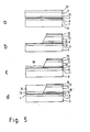
- Fig. 5a The resultant wafer is illustrated in Fig. 5a.
- Fig. 5b the region on the lefthand side of the figure is etched, the rest being masked with an Si0 2 film 70 to expose the n-InP layer 8.
- the properties of sulfuric acid-based etching liquid and hydrochloric acid-based etching liquid can be effectively utilized to selectively etch InGaAsP semiconductor layers and InP semiconductor layers, respectively.
- the result is illustrated in Fig. 5C.
- a second round of LPE growth is achieved to grow a third optical waveguide layer 13 of p-InGaAsP (1.15 micron composition in terms of light wavelength, 0.4 micron thick) and a second cladding layer 14 of p-InP (3 microns thick).
- the resultant state is shown in Fig. 5d.
- a 10 micron current injecting stripe region 100 is opened on the electrode forming layer 12 for injecting an electric current, and then a p-side metal electrode 41 of Au-Zn is formed.
- a p-side metal electrode 41 of Au-Zn is formed.
- an n-side electrode 41 of Au-Ge-Ni is formed, cleaved and cut out to obtain an element having the structure illustrated in Fig. 4.
- the optical waveguide 2 including the first optical waveguide layer 7 of InGaAsP, the third optical waveguide layer 13 and the corrugated layer 4 of InP sandwiched between the two optical waveguide layers, constitutes a distributed Bragg reflector, placed between the InP substrate and the second cladding layer.
- the optical waveguide in the light emitting region adjoining this distributed Bragg reflector includes the first optical waveguide layer 7, the third optical waveguide layer 10, the active layer 9 sandwiched between the two optical waveguide layers, and the InP layer 8 having the same composition as the corrugated layer 4.
- the waveguide in the light emitting region is enclosed by the substrate 6 having a low refractive index and the first cladding layer 11.
- the element When the region containing the active layer 9 and the distributed Bragg reflector section, respectively, are 300 microns and 500 microns long, the element has an oscillation threshold of 150 mA and a differential quantum efficiency of 15 percent on one side, both approximately.
- oscillating wavelength is around 1.30 microns, and a single longitudinal mode is maintained in the injected current region of up to about 2.5 times the oscillation threshold.
- the oscillating wavelength depending on the heat sink temperature, varies at 1.0 ArC. This is a quantity corresponding to the temperature-dependent variation of the refractive index, and is substantially equal to previously reported values.
- the satisfactory oscillation threshold and differential quantum efficiency are attributable to the high reflecting power in the distributed Bragg reflector section.
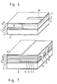
- Fig. 6 shows an oblique view of a second preferred embodiment of the present invention.
- the structure of its distributed Bragg reflector section is the same as in the first embodiment illustrated in Fig. 4. This embodiment differs from the first in that its active layer 9 is produced after the formation of the distributed Bragg reflector section.
- a first optical waveguide layer 7 of n-InGaAsP (1.15 micron composition in terms of light wavelength, 0.2 micron thick) and an n-InP layer 8 (0.1 micron thick) are grown on an n-InP substrate 6 by the first round of LPE growth, a diffraction grating 80 having a period of 1980 A is formed in the n-InP layer 8.
- a third optical waveguide layer 13 of p-InGaAsP (1.15 micron composition in terms of light wavelength, 0.2 micron thick) and a second cladding layer 14 of p-InP (3 microns thick) are laminated.
- partial etching to the-InGaAsP waveguide layer 7 is achieved by the use of hydrochloric acid-based and sulfuric acid-based selective etching liquids.
- a buffer layer 15 of n-InP 0.3 micron thick
- an active layer 9 of non-doped InGaAsP 1.3 micron composition in terms of light wavelength, 0.15 micron thick
- a cladding layer 11 of p-Inp 2.2 micron thick
- an electrode forming layer 12 of p-InGaAsP 1.2 micron composition in terms of light wavelength, 1 micron thick.
- the first optical waveguide layer 7, the corrugated layer 8 and the third optical waveguide layer 13 constitute an optical waveguide, and provide a distributed Bragg reflector. Adjoining the corrugated layer there is arranged the optical active layer 9.
- An element of this structure has substantially the same performance characteristics as the first embodiment, its oscillation threshold being 150 mA and differential quantum efficiency of about 15 percent on one side. Its oscillating wavelength is in a single longitudinal mode in the vicinity of 1.30 microns.
- no waveguide is formed in a plane normal to the laminating direction in the distributed Bragg reflector section. Accordingly, on a small proportion of the light beams which are incident on the distributed Bragg reflector return to the light emitting region of the active layer 9.
- Fig. 7 shows an oblique view of a third preferred embodiment of the present invention, having a buried heterostructure formed on the basis of the structure of the first embodiment.
- a current blocking layer 16 of p-InP (about 0.5 micron thick in its flat part) and a current confining layer 17 of n-InP (about 0.5 micron thick in its flat part) are so grown that they may not grow over the mesa stripe 92.
- an embedding layer 18 of p-InP (1.5 microns thick in its flat part) and an electrode forming layer 12 of p-InGaAsP (1.2 micron composition in terms of light wavelength, 1 micron thick in its flat part) to form a wafer of buried structure (For further details on a buried structure, reference may be made to EP-A-0106305.
- an Si0 2 insulating film 30 is required only over the distributed Bragg reflector section because there is a current confining structure within.
- this structure there is formed, in the mesa stripe 92, a rectangular waveguide extending from the light emitting section including the active layer 9 to the distributed Bragg reflector section. Therefore, most of the light beams diffracted by the distributed Bragg reflector section are returned to the waveguide of the active layer 9.
- the region of the active layer 9 and the distributed Bragg reflector are 300 microns and 500 microns long, respectively, both the oscillation threshold and differential quantum efficiency of the element will be satisfactory, the former being 30 mA and the latter 20 percent on one side.
- Its oscillating wavelength is around 1.30 microns, and has a single mode where the injected current is no more than around three times the threshold.
- the variation of the oscillating wavelength dependent on the temperature variation of the heat sink is about 1 ⁇ rC, i.e. it is substantially equal to those of the first and second embodiments.
- the buried structure can be applied equally effectively to the structure of the second embodiment.
- InP substrates are used in the foregoing embodiments, it also is possible to obtain embodiments of the present invention using an Alx Ga i - x As-based material on a GaAs substrate or an InGaAsP-based material similarly on a GaAs substrate.
Landscapes
- Physics & Mathematics (AREA)
- Condensed Matter Physics & Semiconductors (AREA)
- General Physics & Mathematics (AREA)
- Electromagnetism (AREA)
- Optics & Photonics (AREA)
- Semiconductor Lasers (AREA)
Applications Claiming Priority (2)
| Application Number | Priority Date | Filing Date | Title |
|---|---|---|---|
| JP80378/83 | 1983-05-09 | ||
| JP58080378A JPS59205787A (ja) | 1983-05-09 | 1983-05-09 | 単一軸モ−ド半導体レ−ザ |
Publications (3)
| Publication Number | Publication Date |
|---|---|
| EP0125608A2 EP0125608A2 (en) | 1984-11-21 |
| EP0125608A3 EP0125608A3 (en) | 1986-08-20 |
| EP0125608B1 true EP0125608B1 (en) | 1988-10-12 |
Family
ID=13716616
Family Applications (1)
| Application Number | Title | Priority Date | Filing Date |
|---|---|---|---|
| EP84105167A Expired EP0125608B1 (en) | 1983-05-09 | 1984-05-08 | Single longitudinal mode semiconductor laser |
Country Status (4)
| Country | Link |
|---|---|
| US (1) | US4622674A (ja) |
| EP (1) | EP0125608B1 (ja) |
| JP (1) | JPS59205787A (ja) |
| DE (1) | DE3474616D1 (ja) |
Families Citing this family (20)
| Publication number | Priority date | Publication date | Assignee | Title |
|---|---|---|---|---|
| JPS60260024A (ja) * | 1984-06-07 | 1985-12-23 | Kokusai Denshin Denwa Co Ltd <Kdd> | 光変調素子 |
| US4751710A (en) * | 1984-07-26 | 1988-06-14 | Nec Corporation | Semiconductor laser device |
| JPS61113293A (ja) * | 1984-11-07 | 1986-05-31 | Sharp Corp | 半導体レ−ザアレイ装置 |
| US4747107A (en) * | 1985-09-06 | 1988-05-24 | Bell Communications Research, Inc. | Single mode injection laser |
| JPS62194691A (ja) * | 1986-02-21 | 1987-08-27 | Kokusai Denshin Denwa Co Ltd <Kdd> | 光導波路領域を有する半導体光集積装置の製造方法 |
| JPH0719928B2 (ja) * | 1986-11-26 | 1995-03-06 | 日本電気株式会社 | 光フイルタ素子 |
| JP2587628B2 (ja) * | 1987-01-29 | 1997-03-05 | 国際電信電話株式会社 | 半導体集積発光素子 |
| JPH01186688A (ja) * | 1987-09-02 | 1989-07-26 | Sharp Corp | 半導体レーザ装置 |
| US5147825A (en) * | 1988-08-26 | 1992-09-15 | Bell Telephone Laboratories, Inc. | Photonic-integrated-circuit fabrication process |
| US4932032A (en) * | 1989-08-03 | 1990-06-05 | At&T Bell Laboratories | Tapered semiconductor waveguides |
| US4944838A (en) * | 1989-08-03 | 1990-07-31 | At&T Bell Laboratories | Method of making tapered semiconductor waveguides |
| US5023944A (en) * | 1989-09-05 | 1991-06-11 | General Dynamics Corp./Electronics Division | Optical resonator structures |
| FR2706079B1 (fr) * | 1993-06-02 | 1995-07-21 | France Telecom | Composant intégré monolithique laser-modulateur à structure multi-puits quantiques. |
| GB2354110A (en) * | 1999-09-08 | 2001-03-14 | Univ Bristol | Ridge waveguide lasers |
| US6574260B2 (en) | 2001-03-15 | 2003-06-03 | Corning Lasertron Incorporated | Electroabsorption modulated laser |
| JP2003152274A (ja) * | 2001-11-13 | 2003-05-23 | Furukawa Electric Co Ltd:The | 半導体レーザ装置、半導体レーザモジュールおよびこれを用いたラマン増幅器 |
| CN1312812C (zh) * | 2003-03-03 | 2007-04-25 | 中国科学院半导体研究所 | 波长可调谐分布布拉格反射半导体激光器的制作方法 |
| US8290325B2 (en) * | 2008-06-30 | 2012-10-16 | Intel Corporation | Waveguide photodetector device and manufacturing method thereof |
| US10084282B1 (en) | 2017-08-14 | 2018-09-25 | The United States Of America As Represented By The Secretary Of The Air Force | Fundamental mode operation in broad area quantum cascade lasers |
| US11031753B1 (en) | 2017-11-13 | 2021-06-08 | The Government Of The United States Of America As Represented By The Secretary Of The Air Force | Extracting the fundamental mode in broad area quantum cascade lasers |
Family Cites Families (5)
| Publication number | Priority date | Publication date | Assignee | Title |
|---|---|---|---|---|
| US4045749A (en) * | 1975-11-24 | 1977-08-30 | Xerox Corporation | Corrugation coupled twin guide laser |
| EP0000557B1 (en) * | 1977-08-01 | 1981-12-30 | Hitachi, Ltd. | Semiconductor laser device |
| US4190813A (en) * | 1977-12-28 | 1980-02-26 | Bell Telephone Laboratories, Incorporated | Strip buried heterostructure laser |
| US4464762A (en) * | 1982-02-22 | 1984-08-07 | Bell Telephone Laboratories, Incorporated | Monolithically integrated distributed Bragg reflector laser |
| EP0106305B1 (en) * | 1982-10-12 | 1989-03-15 | Nec Corporation | Double heterostructure semiconductor laser with periodic structure formed in guide layer |
-
1983
- 1983-05-09 JP JP58080378A patent/JPS59205787A/ja active Pending
-
1984
- 1984-05-07 US US06/608,045 patent/US4622674A/en not_active Expired - Fee Related
- 1984-05-08 DE DE8484105167T patent/DE3474616D1/de not_active Expired
- 1984-05-08 EP EP84105167A patent/EP0125608B1/en not_active Expired
Also Published As
| Publication number | Publication date |
|---|---|
| EP0125608A2 (en) | 1984-11-21 |
| EP0125608A3 (en) | 1986-08-20 |
| DE3474616D1 (en) | 1988-11-17 |
| JPS59205787A (ja) | 1984-11-21 |
| US4622674A (en) | 1986-11-11 |
Similar Documents
| Publication | Publication Date | Title |
|---|---|---|
| EP0125608B1 (en) | Single longitudinal mode semiconductor laser | |
| US5457569A (en) | Semiconductor amplifier or laser having integrated lens | |
| EP0169567B1 (en) | Semiconductor laser device | |
| EP0149462B1 (en) | Distributed-feedback semiconductor laser | |
| EP0706243A2 (en) | Distributed feedback semiconductor laser and method for producing the same | |
| CN107230931B (zh) | 分布反馈半导体激光芯片及其制备方法、光模块 | |
| EP0690533B1 (en) | Semiconductor laser having integrated waveguiding lens | |
| JP2746326B2 (ja) | 半導体光素子 | |
| JP2982422B2 (ja) | 半導体レーザおよびその製造方法 | |
| US4775980A (en) | Distributed-feedback semiconductor laser device | |
| CA2165711C (en) | Semiconductor light source having a spectrally broad, high power optical output | |
| EP0106305B1 (en) | Double heterostructure semiconductor laser with periodic structure formed in guide layer | |
| US5469459A (en) | Laser diode element with excellent intermodulation distortion characteristic | |
| KR100456670B1 (ko) | 광 모드 크기 변환기와 분포 궤환형 레이저 다이오드가일체화된 분포 반사형 레이저 다이오드 | |
| JP2001320125A (ja) | 半導体レーザ素子 | |
| US4993035A (en) | High power semiconductor laser using optical integrated circuit | |
| JP2950302B2 (ja) | 半導体レーザ | |
| JPS59119783A (ja) | 半導体発光装置 | |
| JPH0770785B2 (ja) | 分布反射型半導体レーザ | |
| JP3700245B2 (ja) | 位相シフト型分布帰還半導体レーザ | |
| US6734464B2 (en) | Hetero-junction laser diode | |
| JPS63228795A (ja) | 分布帰還型半導体レ−ザ | |
| WO2021148120A1 (en) | Single-mode dfb laser | |
| JP5163355B2 (ja) | 半導体レーザ装置 | |
| JP3595677B2 (ja) | 光アイソレータ、分布帰還型レーザ及び光集積素子 |
Legal Events
| Date | Code | Title | Description |
|---|---|---|---|
| PUAI | Public reference made under article 153(3) epc to a published international application that has entered the european phase |
Free format text: ORIGINAL CODE: 0009012 |
|
| 17P | Request for examination filed |
Effective date: 19840508 |
|
| AK | Designated contracting states |
Designated state(s): DE FR GB |
|
| PUAL | Search report despatched |
Free format text: ORIGINAL CODE: 0009013 |
|
| AK | Designated contracting states |
Kind code of ref document: A3 Designated state(s): DE FR GB |
|
| 17Q | First examination report despatched |
Effective date: 19880115 |
|
| GRAA | (expected) grant |
Free format text: ORIGINAL CODE: 0009210 |
|
| AK | Designated contracting states |
Kind code of ref document: B1 Designated state(s): DE FR GB |
|
| REF | Corresponds to: |
Ref document number: 3474616 Country of ref document: DE Date of ref document: 19881117 |
|
| ET | Fr: translation filed | ||
| PLBE | No opposition filed within time limit |
Free format text: ORIGINAL CODE: 0009261 |
|
| STAA | Information on the status of an ep patent application or granted ep patent |
Free format text: STATUS: NO OPPOSITION FILED WITHIN TIME LIMIT |
|
| 26N | No opposition filed | ||
| PGFP | Annual fee paid to national office [announced via postgrant information from national office to epo] |
Ref country code: GB Payment date: 19950428 Year of fee payment: 12 |
|
| PGFP | Annual fee paid to national office [announced via postgrant information from national office to epo] |
Ref country code: FR Payment date: 19950517 Year of fee payment: 12 |
|
| PGFP | Annual fee paid to national office [announced via postgrant information from national office to epo] |
Ref country code: DE Payment date: 19950728 Year of fee payment: 12 |
|
| PG25 | Lapsed in a contracting state [announced via postgrant information from national office to epo] |
Ref country code: GB Effective date: 19960508 |
|
| GBPC | Gb: european patent ceased through non-payment of renewal fee |
Effective date: 19960508 |
|
| PG25 | Lapsed in a contracting state [announced via postgrant information from national office to epo] |
Ref country code: FR Effective date: 19970131 |
|
| PG25 | Lapsed in a contracting state [announced via postgrant information from national office to epo] |
Ref country code: DE Effective date: 19970201 |
|
| REG | Reference to a national code |
Ref country code: FR Ref legal event code: ST |