EP0121394A2 - Dispositif de mémoire à semi-conducteur incorporant des cellules de mémoire redondantes - Google Patents
Dispositif de mémoire à semi-conducteur incorporant des cellules de mémoire redondantes Download PDFInfo
- Publication number
- EP0121394A2 EP0121394A2 EP84302044A EP84302044A EP0121394A2 EP 0121394 A2 EP0121394 A2 EP 0121394A2 EP 84302044 A EP84302044 A EP 84302044A EP 84302044 A EP84302044 A EP 84302044A EP 0121394 A2 EP0121394 A2 EP 0121394A2
- Authority
- EP
- European Patent Office
- Prior art keywords
- selecting line
- memory cell
- power supply
- memory cells
- set forth
- Prior art date
- Legal status (The legal status is an assumption and is not a legal conclusion. Google has not performed a legal analysis and makes no representation as to the accuracy of the status listed.)
- Granted
Links
Images


Classifications
-
- G—PHYSICS
- G11—INFORMATION STORAGE
- G11C—STATIC STORES
- G11C29/00—Checking stores for correct operation ; Subsequent repair; Testing stores during standby or offline operation
- G11C29/70—Masking faults in memories by using spares or by reconfiguring
- G11C29/78—Masking faults in memories by using spares or by reconfiguring using programmable devices
- G11C29/83—Masking faults in memories by using spares or by reconfiguring using programmable devices with reduced power consumption
-
- G—PHYSICS
- G11—INFORMATION STORAGE
- G11C—STATIC STORES
- G11C11/00—Digital stores characterised by the use of particular electric or magnetic storage elements; Storage elements therefor
- G11C11/21—Digital stores characterised by the use of particular electric or magnetic storage elements; Storage elements therefor using electric elements
- G11C11/34—Digital stores characterised by the use of particular electric or magnetic storage elements; Storage elements therefor using electric elements using semiconductor devices
- G11C11/40—Digital stores characterised by the use of particular electric or magnetic storage elements; Storage elements therefor using electric elements using semiconductor devices using transistors
- G11C11/41—Digital stores characterised by the use of particular electric or magnetic storage elements; Storage elements therefor using electric elements using semiconductor devices using transistors forming static cells with positive feedback, i.e. cells not needing refreshing or charge regeneration, e.g. bistable multivibrator or Schmitt trigger
- G11C11/413—Auxiliary circuits, e.g. for addressing, decoding, driving, writing, sensing, timing or power reduction
- G11C11/417—Auxiliary circuits, e.g. for addressing, decoding, driving, writing, sensing, timing or power reduction for memory cells of the field-effect type
- G11C11/419—Read-write [R-W] circuits
-
- G—PHYSICS
- G11—INFORMATION STORAGE
- G11C—STATIC STORES
- G11C29/00—Checking stores for correct operation ; Subsequent repair; Testing stores during standby or offline operation
- G11C29/70—Masking faults in memories by using spares or by reconfiguring
- G11C29/78—Masking faults in memories by using spares or by reconfiguring using programmable devices
- G11C29/83—Masking faults in memories by using spares or by reconfiguring using programmable devices with reduced power consumption
- G11C29/832—Masking faults in memories by using spares or by reconfiguring using programmable devices with reduced power consumption with disconnection of faulty elements
-
- G—PHYSICS
- G11—INFORMATION STORAGE
- G11C—STATIC STORES
- G11C7/00—Arrangements for writing information into, or reading information out from, a digital store
- G11C7/12—Bit line control circuits, e.g. drivers, boosters, pull-up circuits, pull-down circuits, precharging circuits, equalising circuits, for bit lines
-
- G—PHYSICS
- G11—INFORMATION STORAGE
- G11C—STATIC STORES
- G11C8/00—Arrangements for selecting an address in a digital store
- G11C8/18—Address timing or clocking circuits; Address control signal generation or management, e.g. for row address strobe [RAS] or column address strobe [CAS] signals
Definitions
- the present invention relates to a static semiconductor memory device incorporating redundancy memory cells.
- a large number of memory cells are arranged along rows and columns.
- the density of defects generated in such a semiconductor memory device during the manufacture thereof is relatively independent of the integration density of the device. Rather, it derives from the semiconductor manufacturing technology. In general, the higher the integration density of the device, the greater the ratio of normal memory cells to defective memory cells. This is one of the advantages of increasing the integration density of a semiconductor memory device.
- redundancy/memory cells use is made of redundancy/memory cells.
- a redundancy memory cell row or column is selected instead of the memory cell row or column including the defective memory cell.
- one or two redundancy memory cell rows or columns are usually provided.
- a problem in the prior art has been that when the defective memory cell has a direct current (DC) defect, i.e., when the defective memory cell is short-circuited, the DC defect itself is not resolved even when a redundancy memory cell row or column is selected.
- DC direct current
- An embodiment of the present invention can provide a static semiconductor memory device incorporating redundancy memory cells in which DC defects themselves are substantially resolved.
- a static semiconductor memory device comprising:
- the potential of a clock signal is applied to loads linked between bit line pairs and a power supply at least during a non-selected state (stand-by state) so as to cut off currents flowing through the loads, thereby reducing the load current of bit lines for all memory cells, including a defective memory cell. That is, even when the defective memory cell has a DC defect, power supply currents due to the DC defect are suppressed, thereby substantially resolving the DC defect.
- fuses are provided between the bit line pairs and the power supply. When a defective memory cell is detected, fuses corresponding to this defective memory cell are melted so as to cut off currents flowing to the defective memory cell, thereby completely resolving the DC defect.
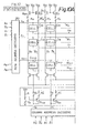
- Fig. 1 which illustrates a prior art static semiconductor memory device
- Each memory cell is connected to one word line, a hold line and a pair of bit lines.
- a memory cell C 00 is connected to a word line W 0 , to a hold line H 0 , and to bit lines B 0 and B 0 .
- a series of memory cells C OR , C 1R , ..., C n-1,R are arranged along the column direction. These memory cells C 0R , C 1R , ..., C n-1,R serve as redundancy memory cells.
- the hold lines H 0 , H 1 , ..., H n-1 are connected to earth, which serves as one of the power supplies.
- the bit lines B 0 , B 0 , B 1 , B 1 , ..., B n-1 , B n-1 , B R , and B R are connected via load transistors Q L0 , Q L0 , Q L1 , Q L1 , ..., Q LR ' Q LR to a power supply V CC .
- the load transistors are, for example, enhancement metal-insulator-semiconductor (MIS) transistors.
- Reference CD 1 designates column decoders
- CD 2 designates a decoder for selecting the redundancy memory cells.
- the decoder CD 2 is comprised of a resistor R, fuses F X , F 0 , F 0 , F 1 , F 1 , ..., F n-1, F n-1 , and transistors Q X0 , Q X1 , ..., Q Xn-1 .
- S A is a sense amplifier
- OB is an output buffer
- D out is output data
- a 0 ' , A 0 ' , A 1 ' , A 1 , ..., A l-1 , and A l-1 ' are column address signals.
- the memory cell C 00 is comprised of resistors R 1 and R 2 , driver transistors Q 1 and Q 2 , and transfer transistors Q 3 and Q 4 . Therefore, when a DC defect is generated so as to short-circuit the bit line B O or B O to the hold line H O , a current flows from the power supply V CC via the load transistor Q L and the short-circuited portion to the hold line H O even when the redundancy memory cell C OR is selected instead of the memory cell C OO . Therefore, the DC defect itself. is not resolved.
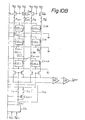
- the power supply voltage V CC is also applied to the gates of the load transistors Q L0 , Q L0 , Q L1 , Q L1 , ..., Q L,n-1 , Q L,n-1 , Q LR , Q LR .
- a clock signal ⁇ is applied to the gates of the transistors Q L0 .
- the potential of the clock signal ⁇ is made low at least during a non-selected state, thereby preventing currents from flowing from the power supply V CC to all the memory cells.
- the above-mentioned clock signal (pulse signal) ⁇ is obtained as an inversion signal of a chip select signal CS . That is, the clock signal ⁇ is easily obtained by using an inverter G 0 as shown in Fig. 5.
- the potential of the clock signal ⁇ is, in this case, low, so that all the load transistors are cut off.
- a current flowing through the defective portion in the case of the potential of the clock signal ⁇ being high is extremely small as compared with the total power consumption of the semiconductor device.
- Figures 6A, 6B, and 6C are also timing diagrams for explaining the generation of the clock signal ⁇ of Fig. 3.
- the clock signal ⁇ as shown in Fig. 6C becomes high for a definite (short) time period only after the chip select signal CS as shown in Fig. 6A is changed or after one ADD of the row address signals A 0 , A 1 , ..., and A l-1 is changed. Therefore, the current flowing from the power supply V CC to the above-mentioned defective portion is of shorter duration than with the signal as shown in Fig. 4B.
- the clock signal ⁇ as shown in Fig. 6C can be obtained by a pulse generating circuit PG of Fig. 7. That is, in Fig. 7, the pulse generating circuit PG comprises a plurality of clock pulse generating circuits PG 0 , PG 1 , ..., PG l-1 , and PG t corresponding to each of the row address signals A 0 , A 1 , ..., A l-1 , and the chip select signal CS. Therefore, when one of the signals A 0 , A 1 , ..., A l-1 , and CS is changed, for example, when the signal A 0 is changed, the clock pulse generating circuit PG O generates the clock signal 6 via an OR circuit OR. That is, when the device of Fig. 3 is changed from a non-selected state to a selected state or vice versa, or when the selected row is changed, the pulse generating circuit PG generates the clock signal ⁇ .
- Fig. 8 which is a detailed logic circuit diagram of one of the clock pulse generating circuits PG i of the pulse generating circuit PG of Fig. 7, references G 1 to G 4 are NAND gates, G 5 and G 6 NOR gates, G 7 an OR gate, and C l and C 2 capacitors. Operation will be explained below with reference to Figs. 9A to 9H.
- the address signal A i node a
- the output b of the NAND gate G 1 changes as shown in Fig. 9B
- the output d of the NAND gate G 2 is an inverted signal of the signal b which is delayed a little by the capacitor C 1 , as shown in Fig. 9D.
- the output f of the NOR gate G 5 is a pulse which is generated by the rise of the address signal A. , as shown in Fig. 9E.
- the output g of the NOR gate G 6 is a signal which is generated by the fall of the address signal A i , as shown in Fig. 9G. Therefore, as shown in Fig. 9H the output CP i of the OR gate G 7 , which combines the signal f with the signal g, is a clock signal which is generated by the change of the address signal A 0 , A 1 , ..., A l-1 , or the signal CS. in duration
- the bit line load currents are reduced/, the power supply currents flowing through a defective memory cell can be reduced, even when the defective memory cell has a DC defect. Therefore, the DC defect can be substantially resolved.
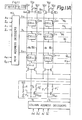
- fuses F 10 , F 10 , F 11 , F 11 , .. ., F 1,n-1 , F 1,n-1 , F 1R , and F 1R are added to the elements of Fig. 1.
- Each fuse is provided between the memory cells and the power supply V CC .
- each fuse can be provided on the drain side of the load transistor (between drain and V CC ) as well as on the source side (between source and bit line) thereof. In either case, the same effect is exhibited.
- the fuses F X , F 0 , F 1 ' , ..., and F n-1 ' are melted in the same way as stated above.
- the fuses F 10 and F 10 are melted. Therefore, even when the memory cell C OO has a DC defect, no current flows from the power supply V CC via the memory cell C OO to the hold line H O . This means that the DC defect is completely resolved.
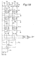
- fuses F 20 , F 21 ' ..., F 2,n-1 , and F 2R are added to the elements of Fig. 1. This case is equivalent to that wherein each fuse is provided between the memory cells and the power supply V CC .
- the fuses F X , F 0 , F 1 ' , ..., and F n-1 ' are melted in the same way as stated above.
- the fuse F 20 is melted, thereby producing the same result as in the Fig. 10 embodiment.
Landscapes
- Engineering & Computer Science (AREA)
- Microelectronics & Electronic Packaging (AREA)
- Computer Hardware Design (AREA)
- For Increasing The Reliability Of Semiconductor Memories (AREA)
- Static Random-Access Memory (AREA)
Applications Claiming Priority (4)
| Application Number | Priority Date | Filing Date | Title |
|---|---|---|---|
| JP50347/83 | 1983-03-28 | ||
| JP58050347A JPH0652639B2 (ja) | 1983-03-28 | 1983-03-28 | 半導体記憶装置 |
| JP51535/83 | 1983-03-29 | ||
| JP58051535A JPS59178691A (ja) | 1983-03-29 | 1983-03-29 | 半導体記憶装置 |
Publications (3)
| Publication Number | Publication Date |
|---|---|
| EP0121394A2 true EP0121394A2 (fr) | 1984-10-10 |
| EP0121394A3 EP0121394A3 (en) | 1988-01-27 |
| EP0121394B1 EP0121394B1 (fr) | 1991-10-23 |
Family
ID=26390811
Family Applications (1)
| Application Number | Title | Priority Date | Filing Date |
|---|---|---|---|
| EP19840302044 Expired - Lifetime EP0121394B1 (fr) | 1983-03-28 | 1984-03-27 | Dispositif de mémoire à semi-conducteur incorporant des cellules de mémoire redondantes |
Country Status (3)
| Country | Link |
|---|---|
| US (1) | US4587639A (fr) |
| EP (1) | EP0121394B1 (fr) |
| DE (1) | DE3485188D1 (fr) |
Cited By (8)
| Publication number | Priority date | Publication date | Assignee | Title |
|---|---|---|---|---|
| EP0186175A2 (fr) * | 1984-12-24 | 1986-07-02 | Nec Corporation | Dispositif de mémoire à semi-conducteur ayant une structure à redondance |
| FR2576133A1 (fr) * | 1985-01-15 | 1986-07-18 | Eurotechnique Sa | Memoire en circuit integre a haute fiabilite |
| EP0258715A2 (fr) * | 1986-08-15 | 1988-03-09 | Nec Corporation | Mémoire statique à accès aléatoire d'une construction Bi-CMOS |
| EP0414477A2 (fr) * | 1989-08-25 | 1991-02-27 | Fujitsu Limited | Dispositif de mémoire à semiconducteur ayant des cellules de mémoire redondantes |
| DE4105104A1 (de) * | 1990-02-21 | 1991-08-22 | Mitsubishi Electric Corp | Halbleiterspeichereinrichtung und verfahren zur fehlerkorrektur |
| EP0486295A2 (fr) * | 1990-11-16 | 1992-05-20 | Nec Corporation | Dispositif de mémoire à semi-conducteur à circuit de redondance |
| EP0619545A2 (fr) * | 1993-04-08 | 1994-10-12 | Sharp Kabushiki Kaisha | Procédé et appareil de réparation de mémoire au moyen de la redondance |
| EP0747824A1 (fr) * | 1995-06-07 | 1996-12-11 | STMicroelectronics, Inc. | Circuit et méthode pour la polarisation de lignes de bit |
Families Citing this family (11)
| Publication number | Priority date | Publication date | Assignee | Title |
|---|---|---|---|---|
| US5687109A (en) * | 1988-05-31 | 1997-11-11 | Micron Technology, Inc. | Integrated circuit module having on-chip surge capacitors |
| US5235548A (en) * | 1989-04-13 | 1993-08-10 | Dallas Semiconductor Corp. | Memory with power supply intercept in redundancy logic |
| US5471427A (en) * | 1989-06-05 | 1995-11-28 | Mitsubishi Denki Kabushiki Kaisha | Circuit for repairing defective bit in semiconductor memory device and repairing method |
| JP3115623B2 (ja) * | 1991-02-25 | 2000-12-11 | 株式会社日立製作所 | スタティック型ram |
| JP2888034B2 (ja) * | 1991-06-27 | 1999-05-10 | 日本電気株式会社 | 半導体メモリ装置 |
| KR0157339B1 (ko) * | 1995-06-28 | 1998-12-01 | 김광호 | 반도체 메모리의 불량셀 구제회로 |
| US6249464B1 (en) | 1999-12-15 | 2001-06-19 | Cypress Semiconductor Corp. | Block redundancy in ultra low power memory circuits |
| KR100320683B1 (ko) * | 2000-02-03 | 2002-01-17 | 윤종용 | 스탠바이 전류불량 구제기능을 가지는 반도체 메모리 장치 |
| US7117400B2 (en) * | 2002-11-13 | 2006-10-03 | International Business Machines Corporation | Memory device with data line steering and bitline redundancy |
| TWI242213B (en) * | 2003-09-09 | 2005-10-21 | Winbond Electronics Corp | Device and method of leakage current cuter and memory cell and memory device thereof |
| DE602005013964D1 (de) * | 2005-09-29 | 2009-05-28 | Qimonda Ag | Speicher mit Widerstandspeicherzellenmatrix und Bitleitungsaufladung |
Citations (3)
| Publication number | Priority date | Publication date | Assignee | Title |
|---|---|---|---|---|
| US4053873A (en) * | 1976-06-30 | 1977-10-11 | International Business Machines Corporation | Self-isolating cross-coupled sense amplifier latch circuit |
| US4247921A (en) * | 1978-07-31 | 1981-01-27 | Fujitsu Limited | Decoder |
| EP0095721A2 (fr) * | 1982-05-28 | 1983-12-07 | Kabushiki Kaisha Toshiba | Dispositif de mémoire à semi-conducteur |
Family Cites Families (2)
| Publication number | Priority date | Publication date | Assignee | Title |
|---|---|---|---|---|
| US4228528B2 (en) * | 1979-02-09 | 1992-10-06 | Memory with redundant rows and columns | |
| US4281398A (en) * | 1980-02-12 | 1981-07-28 | Mostek Corporation | Block redundancy for memory array |
-
1984
- 1984-03-27 DE DE8484302044T patent/DE3485188D1/de not_active Expired - Fee Related
- 1984-03-27 US US06/593,771 patent/US4587639A/en not_active Expired - Lifetime
- 1984-03-27 EP EP19840302044 patent/EP0121394B1/fr not_active Expired - Lifetime
Patent Citations (3)
| Publication number | Priority date | Publication date | Assignee | Title |
|---|---|---|---|---|
| US4053873A (en) * | 1976-06-30 | 1977-10-11 | International Business Machines Corporation | Self-isolating cross-coupled sense amplifier latch circuit |
| US4247921A (en) * | 1978-07-31 | 1981-01-27 | Fujitsu Limited | Decoder |
| EP0095721A2 (fr) * | 1982-05-28 | 1983-12-07 | Kabushiki Kaisha Toshiba | Dispositif de mémoire à semi-conducteur |
Non-Patent Citations (3)
| Title |
|---|
| IEEE JOURNAL OF SOLID-STATE CIRCUITS, vol. SC-16, no. 5, October 1981, pages 435-443, IEEE, New York, US; K.C. HARDEE et al.: "A fault-tolerant 30 ns/375 mW 16K x 1 NMOS static RAM" * |
| IEEE JOURNAL OF SOLID-STATE CIRCUITS, vol. SC-17, no. 5, October 1982, pages 798-803, IEEE, New York, US; K. OCHII et al: "An ultralow power 8K x 8-bit full CMOS RAM with a six-transistor cell" * |
| IEEE JOURNAL OF SOLID-STATE CIRCUITS, vol. SC-17, no. 5, October 1982, pages 804-809, IEEE, New York, US; Y. UCHIDA et al.: "A low power resistive load 64 kbit CMOS RAM" * |
Cited By (18)
| Publication number | Priority date | Publication date | Assignee | Title |
|---|---|---|---|---|
| EP0186175A2 (fr) * | 1984-12-24 | 1986-07-02 | Nec Corporation | Dispositif de mémoire à semi-conducteur ayant une structure à redondance |
| EP0186175A3 (fr) * | 1984-12-24 | 1989-02-08 | Nec Corporation | Dispositif de mémoire à semi-conducteur ayant une structure à redondance |
| FR2576133A1 (fr) * | 1985-01-15 | 1986-07-18 | Eurotechnique Sa | Memoire en circuit integre a haute fiabilite |
| EP0258715A2 (fr) * | 1986-08-15 | 1988-03-09 | Nec Corporation | Mémoire statique à accès aléatoire d'une construction Bi-CMOS |
| EP0258715A3 (en) * | 1986-08-15 | 1990-07-04 | Nec Corporation | Static random access memory having bi-cmos construction |
| EP0523756A3 (en) * | 1986-08-15 | 1993-06-09 | Nec Corporation | Static random access memory having bi-cmos construction |
| EP0523756A2 (fr) * | 1986-08-15 | 1993-01-20 | Nec Corporation | Mémoire statique à accès aléatoire de construction Bi-CMOS |
| EP0414477A3 (en) * | 1989-08-25 | 1992-08-05 | Fujitsu Limited | Semiconductor memory device having redundant memory cells |
| US5197030A (en) * | 1989-08-25 | 1993-03-23 | Fujitsu Limited | Semiconductor memory device having redundant memory cells |
| EP0414477A2 (fr) * | 1989-08-25 | 1991-02-27 | Fujitsu Limited | Dispositif de mémoire à semiconducteur ayant des cellules de mémoire redondantes |
| DE4105104A1 (de) * | 1990-02-21 | 1991-08-22 | Mitsubishi Electric Corp | Halbleiterspeichereinrichtung und verfahren zur fehlerkorrektur |
| US5315551A (en) * | 1990-02-21 | 1994-05-24 | Mitsubishi Denki Kabushiki Kaisha | Semiconductor memory device with precharging voltage level unchanged by defective memory cell |
| DE4105104C3 (de) * | 1990-02-21 | 1998-10-22 | Mitsubishi Electric Corp | Halbleiterspeichereinrichtung und Verfahren zur Fehlerkorrektur |
| EP0486295A2 (fr) * | 1990-11-16 | 1992-05-20 | Nec Corporation | Dispositif de mémoire à semi-conducteur à circuit de redondance |
| EP0486295A3 (en) * | 1990-11-16 | 1993-07-28 | Nec Corporation | Semiconductor memory device with redundant circuit |
| EP0619545A2 (fr) * | 1993-04-08 | 1994-10-12 | Sharp Kabushiki Kaisha | Procédé et appareil de réparation de mémoire au moyen de la redondance |
| EP0619545A3 (fr) * | 1993-04-08 | 1996-10-16 | Sharp Kk | Procédé et appareil de réparation de mémoire au moyen de la redondance. |
| EP0747824A1 (fr) * | 1995-06-07 | 1996-12-11 | STMicroelectronics, Inc. | Circuit et méthode pour la polarisation de lignes de bit |
Also Published As
| Publication number | Publication date |
|---|---|
| EP0121394A3 (en) | 1988-01-27 |
| US4587639A (en) | 1986-05-06 |
| EP0121394B1 (fr) | 1991-10-23 |
| DE3485188D1 (de) | 1991-11-28 |
Similar Documents
| Publication | Publication Date | Title |
|---|---|---|
| US4837747A (en) | Redundary circuit with a spare main decoder responsive to an address of a defective cell in a selected cell block | |
| US4587639A (en) | Static semiconductor memory device incorporating redundancy memory cells | |
| US4365319A (en) | Semiconductor memory device | |
| EP0293339B1 (fr) | Dispositif de mémoire permanente supportant un grand nombre de cycles de programmation | |
| EP0031386B1 (fr) | Dispositif de memoire a semi-conducteurs | |
| US5258953A (en) | Semiconductor memory device | |
| US4839864A (en) | Semiconductor memory device comprising programmable redundancy circuit | |
| US4658379A (en) | Semiconductor memory device with a laser programmable redundancy circuit | |
| EP0376245A2 (fr) | Dispositif de mémoire à semi-conducteurs muni d'un décodeur redondant | |
| JP3821992B2 (ja) | 半導体メモリ装置の冗長デコーダイネイブル回路 | |
| US4987560A (en) | Semiconductor memory device | |
| EP0115140B1 (fr) | Circuit décodeur | |
| US6535438B2 (en) | Semiconductor memory device adopting redundancy system | |
| JPH11232869A (ja) | 半導体回路装置 | |
| JP2760326B2 (ja) | 半導体記憶装置 | |
| US7505339B2 (en) | Static semiconductor memory device allowing simultaneous writing of data into a plurality of memory cells | |
| US5528540A (en) | Redundant address decoder | |
| KR100210627B1 (ko) | 반도체 메모리 장치 | |
| US6307772B1 (en) | Static type semiconductor memory device for lower current consumption | |
| US6392956B2 (en) | Semiconductor memory that enables high speed operation | |
| KR900008659B1 (ko) | 용장성 구조를 갖춘 바이폴러 트랜지스터형 랜덤 액세스 메모리 | |
| JPS6350799B2 (fr) | ||
| US4593383A (en) | Integated circuit memory | |
| JP2002184194A (ja) | 半導体メモリ装置の欠陥アドレス貯蔵回路 | |
| US6392940B2 (en) | Semiconductor memory circuit |
Legal Events
| Date | Code | Title | Description |
|---|---|---|---|
| PUAI | Public reference made under article 153(3) epc to a published international application that has entered the european phase |
Free format text: ORIGINAL CODE: 0009012 |
|
| AK | Designated contracting states |
Designated state(s): DE FR GB |
|
| RIN1 | Information on inventor provided before grant (corrected) |
Inventor name: YAMAUCHI, TAKAHIKO Inventor name: SEKI, TERUO DAI-2 YAYOI-SO 5 Inventor name: AOYAMA, KEIZO |
|
| PUAL | Search report despatched |
Free format text: ORIGINAL CODE: 0009013 |
|
| AK | Designated contracting states |
Kind code of ref document: A3 Designated state(s): DE FR GB |
|
| 17P | Request for examination filed |
Effective date: 19880609 |
|
| 17Q | First examination report despatched |
Effective date: 19891010 |
|
| GRAA | (expected) grant |
Free format text: ORIGINAL CODE: 0009210 |
|
| AK | Designated contracting states |
Kind code of ref document: B1 Designated state(s): DE FR GB |
|
| REF | Corresponds to: |
Ref document number: 3485188 Country of ref document: DE Date of ref document: 19911128 |
|
| ET | Fr: translation filed | ||
| RIN2 | Information on inventor provided after grant (corrected) |
Free format text: AOYAMA, KEIZO * SEKI, TERUO DAI-2 YAYOI-SO 5 * YAMAUCHI, TAKAHIKO |
|
| PLBE | No opposition filed within time limit |
Free format text: ORIGINAL CODE: 0009261 |
|
| STAA | Information on the status of an ep patent application or granted ep patent |
Free format text: STATUS: NO OPPOSITION FILED WITHIN TIME LIMIT |
|
| 26N | No opposition filed | ||
| REG | Reference to a national code |
Ref country code: GB Ref legal event code: IF02 |
|
| PGFP | Annual fee paid to national office [announced via postgrant information from national office to epo] |
Ref country code: FR Payment date: 20020312 Year of fee payment: 19 |
|
| PGFP | Annual fee paid to national office [announced via postgrant information from national office to epo] |
Ref country code: GB Payment date: 20020327 Year of fee payment: 19 |
|
| PGFP | Annual fee paid to national office [announced via postgrant information from national office to epo] |
Ref country code: DE Payment date: 20020404 Year of fee payment: 19 |
|
| PG25 | Lapsed in a contracting state [announced via postgrant information from national office to epo] |
Ref country code: GB Free format text: LAPSE BECAUSE OF NON-PAYMENT OF DUE FEES Effective date: 20030327 |
|
| PG25 | Lapsed in a contracting state [announced via postgrant information from national office to epo] |
Ref country code: DE Free format text: LAPSE BECAUSE OF NON-PAYMENT OF DUE FEES Effective date: 20031001 |
|
| GBPC | Gb: european patent ceased through non-payment of renewal fee |
Effective date: 20030327 |
|
| PG25 | Lapsed in a contracting state [announced via postgrant information from national office to epo] |
Ref country code: FR Free format text: LAPSE BECAUSE OF NON-PAYMENT OF DUE FEES Effective date: 20031127 |
|
| REG | Reference to a national code |
Ref country code: FR Ref legal event code: ST |