EP0113434B2 - Photovoltaic device - Google Patents
Photovoltaic device Download PDFInfo
- Publication number
- EP0113434B2 EP0113434B2 EP83112159A EP83112159A EP0113434B2 EP 0113434 B2 EP0113434 B2 EP 0113434B2 EP 83112159 A EP83112159 A EP 83112159A EP 83112159 A EP83112159 A EP 83112159A EP 0113434 B2 EP0113434 B2 EP 0113434B2
- Authority
- EP
- European Patent Office
- Prior art keywords
- region
- amorphous
- crystalline
- solar cell
- type
- Prior art date
- Legal status (The legal status is an assumption and is not a legal conclusion. Google has not performed a legal analysis and makes no representation as to the accuracy of the status listed.)
- Expired - Lifetime
Links
- 239000004065 semiconductor Substances 0.000 claims description 82
- 229910021417 amorphous silicon Inorganic materials 0.000 claims description 44
- 239000000758 substrate Substances 0.000 claims description 18
- 239000010409 thin film Substances 0.000 claims description 15
- 229910010271 silicon carbide Inorganic materials 0.000 claims description 14
- 229910004541 SiN Inorganic materials 0.000 claims description 13
- 229910003465 moissanite Inorganic materials 0.000 claims description 13
- 229910000577 Silicon-germanium Inorganic materials 0.000 claims description 11
- 229910021424 microcrystalline silicon Inorganic materials 0.000 claims description 9
- 230000003247 decreasing effect Effects 0.000 claims description 5
- 230000001788 irregular Effects 0.000 claims description 4
- 229910010272 inorganic material Inorganic materials 0.000 claims description 3
- 239000011147 inorganic material Substances 0.000 claims description 3
- 239000011368 organic material Substances 0.000 claims 2
- 238000000034 method Methods 0.000 description 33
- 238000006243 chemical reaction Methods 0.000 description 17
- 239000000463 material Substances 0.000 description 15
- 239000010408 film Substances 0.000 description 13
- 229910021420 polycrystalline silicon Inorganic materials 0.000 description 13
- CIWBSHSKHKDKBQ-JLAZNSOCSA-N Ascorbic acid Chemical compound OC[C@H](O)[C@H]1OC(=O)C(O)=C1O CIWBSHSKHKDKBQ-JLAZNSOCSA-N 0.000 description 11
- 238000004519 manufacturing process Methods 0.000 description 11
- 229910001218 Gallium arsenide Inorganic materials 0.000 description 7
- 238000010586 diagram Methods 0.000 description 7
- 229910021421 monocrystalline silicon Inorganic materials 0.000 description 7
- HBMJWWWQQXIZIP-UHFFFAOYSA-N silicon carbide Chemical compound [Si+]#[C-] HBMJWWWQQXIZIP-UHFFFAOYSA-N 0.000 description 6
- 239000012535 impurity Substances 0.000 description 5
- 238000005229 chemical vapour deposition Methods 0.000 description 4
- 238000000151 deposition Methods 0.000 description 4
- 238000010521 absorption reaction Methods 0.000 description 3
- 229910052782 aluminium Inorganic materials 0.000 description 3
- XAGFODPZIPBFFR-UHFFFAOYSA-N aluminium Chemical compound [Al] XAGFODPZIPBFFR-UHFFFAOYSA-N 0.000 description 3
- AMGQUBHHOARCQH-UHFFFAOYSA-N indium;oxotin Chemical compound [In].[Sn]=O AMGQUBHHOARCQH-UHFFFAOYSA-N 0.000 description 3
- 229910052710 silicon Inorganic materials 0.000 description 3
- 239000007787 solid Substances 0.000 description 3
- 230000007704 transition Effects 0.000 description 3
- 239000004642 Polyimide Substances 0.000 description 2
- 229910020328 SiSn Inorganic materials 0.000 description 2
- XUIMIQQOPSSXEZ-UHFFFAOYSA-N Silicon Chemical compound [Si] XUIMIQQOPSSXEZ-UHFFFAOYSA-N 0.000 description 2
- 239000000919 ceramic Substances 0.000 description 2
- 239000002178 crystalline material Substances 0.000 description 2
- 229910021419 crystalline silicon Inorganic materials 0.000 description 2
- 230000008021 deposition Effects 0.000 description 2
- 238000009792 diffusion process Methods 0.000 description 2
- SCCCLDWUZODEKG-UHFFFAOYSA-N germanide Chemical compound [GeH3-] SCCCLDWUZODEKG-UHFFFAOYSA-N 0.000 description 2
- 229910052732 germanium Inorganic materials 0.000 description 2
- 239000011521 glass Substances 0.000 description 2
- PJXISJQVUVHSOJ-UHFFFAOYSA-N indium(iii) oxide Chemical compound [O-2].[O-2].[O-2].[In+3].[In+3] PJXISJQVUVHSOJ-UHFFFAOYSA-N 0.000 description 2
- 238000005468 ion implantation Methods 0.000 description 2
- 238000007733 ion plating Methods 0.000 description 2
- 150000002500 ions Chemical class 0.000 description 2
- 229910052751 metal Inorganic materials 0.000 description 2
- 239000002184 metal Substances 0.000 description 2
- 229920001721 polyimide Polymers 0.000 description 2
- 239000010703 silicon Substances 0.000 description 2
- 238000001228 spectrum Methods 0.000 description 2
- 238000004544 sputter deposition Methods 0.000 description 2
- 229910001220 stainless steel Inorganic materials 0.000 description 2
- 239000010935 stainless steel Substances 0.000 description 2
- 238000006467 substitution reaction Methods 0.000 description 2
- JBRZTFJDHDCESZ-UHFFFAOYSA-N AsGa Chemical compound [As]#[Ga] JBRZTFJDHDCESZ-UHFFFAOYSA-N 0.000 description 1
- 229910004613 CdTe Inorganic materials 0.000 description 1
- 206010034960 Photophobia Diseases 0.000 description 1
- 206010034972 Photosensitivity reaction Diseases 0.000 description 1
- 238000000137 annealing Methods 0.000 description 1
- 125000004429 atom Chemical group 0.000 description 1
- 230000015572 biosynthetic process Effects 0.000 description 1
- 229910052980 cadmium sulfide Inorganic materials 0.000 description 1
- 239000000969 carrier Substances 0.000 description 1
- 239000000470 constituent Substances 0.000 description 1
- 239000013078 crystal Substances 0.000 description 1
- 238000000354 decomposition reaction Methods 0.000 description 1
- 230000006866 deterioration Effects 0.000 description 1
- 230000000694 effects Effects 0.000 description 1
- 230000005684 electric field Effects 0.000 description 1
- 230000002708 enhancing effect Effects 0.000 description 1
- 239000007789 gas Substances 0.000 description 1
- GNPVGFCGXDBREM-UHFFFAOYSA-N germanium atom Chemical compound [Ge] GNPVGFCGXDBREM-UHFFFAOYSA-N 0.000 description 1
- APFVFJFRJDLVQX-UHFFFAOYSA-N indium atom Chemical group [In] APFVFJFRJDLVQX-UHFFFAOYSA-N 0.000 description 1
- 229910003480 inorganic solid Inorganic materials 0.000 description 1
- 230000031700 light absorption Effects 0.000 description 1
- 208000013469 light sensitivity Diseases 0.000 description 1
- 239000011159 matrix material Substances 0.000 description 1
- 239000007769 metal material Substances 0.000 description 1
- 238000001451 molecular beam epitaxy Methods 0.000 description 1
- 230000003287 optical effect Effects 0.000 description 1
- 125000004430 oxygen atom Chemical group O* 0.000 description 1
- 230000036211 photosensitivity Effects 0.000 description 1
- 238000005215 recombination Methods 0.000 description 1
- 230000006798 recombination Effects 0.000 description 1
- HQVNEWCFYHHQES-UHFFFAOYSA-N silicon nitride Chemical compound N12[Si]34N5[Si]62N3[Si]51N64 HQVNEWCFYHHQES-UHFFFAOYSA-N 0.000 description 1
- 229910001134 stannide Inorganic materials 0.000 description 1
- 238000001771 vacuum deposition Methods 0.000 description 1
- 238000005019 vapor deposition process Methods 0.000 description 1
Images


Classifications
-
- H—ELECTRICITY
- H01—ELECTRIC ELEMENTS
- H01L—SEMICONDUCTOR DEVICES NOT COVERED BY CLASS H10
- H01L31/00—Semiconductor devices sensitive to infrared radiation, light, electromagnetic radiation of shorter wavelength or corpuscular radiation and specially adapted either for the conversion of the energy of such radiation into electrical energy or for the control of electrical energy by such radiation; Processes or apparatus specially adapted for the manufacture or treatment thereof or of parts thereof; Details thereof
- H01L31/04—Semiconductor devices sensitive to infrared radiation, light, electromagnetic radiation of shorter wavelength or corpuscular radiation and specially adapted either for the conversion of the energy of such radiation into electrical energy or for the control of electrical energy by such radiation; Processes or apparatus specially adapted for the manufacture or treatment thereof or of parts thereof; Details thereof adapted as photovoltaic [PV] conversion devices
- H01L31/06—Semiconductor devices sensitive to infrared radiation, light, electromagnetic radiation of shorter wavelength or corpuscular radiation and specially adapted either for the conversion of the energy of such radiation into electrical energy or for the control of electrical energy by such radiation; Processes or apparatus specially adapted for the manufacture or treatment thereof or of parts thereof; Details thereof adapted as photovoltaic [PV] conversion devices characterised by at least one potential-jump barrier or surface barrier
- H01L31/072—Semiconductor devices sensitive to infrared radiation, light, electromagnetic radiation of shorter wavelength or corpuscular radiation and specially adapted either for the conversion of the energy of such radiation into electrical energy or for the control of electrical energy by such radiation; Processes or apparatus specially adapted for the manufacture or treatment thereof or of parts thereof; Details thereof adapted as photovoltaic [PV] conversion devices characterised by at least one potential-jump barrier or surface barrier the potential barriers being only of the PN heterojunction type
- H01L31/0745—Semiconductor devices sensitive to infrared radiation, light, electromagnetic radiation of shorter wavelength or corpuscular radiation and specially adapted either for the conversion of the energy of such radiation into electrical energy or for the control of electrical energy by such radiation; Processes or apparatus specially adapted for the manufacture or treatment thereof or of parts thereof; Details thereof adapted as photovoltaic [PV] conversion devices characterised by at least one potential-jump barrier or surface barrier the potential barriers being only of the PN heterojunction type comprising a AIVBIV heterojunction, e.g. Si/Ge, SiGe/Si or Si/SiC solar cells
- H01L31/0747—Semiconductor devices sensitive to infrared radiation, light, electromagnetic radiation of shorter wavelength or corpuscular radiation and specially adapted either for the conversion of the energy of such radiation into electrical energy or for the control of electrical energy by such radiation; Processes or apparatus specially adapted for the manufacture or treatment thereof or of parts thereof; Details thereof adapted as photovoltaic [PV] conversion devices characterised by at least one potential-jump barrier or surface barrier the potential barriers being only of the PN heterojunction type comprising a AIVBIV heterojunction, e.g. Si/Ge, SiGe/Si or Si/SiC solar cells comprising a heterojunction of crystalline and amorphous materials, e.g. heterojunction with intrinsic thin layer or HIT® solar cells; solar cells
-
- H—ELECTRICITY
- H01—ELECTRIC ELEMENTS
- H01L—SEMICONDUCTOR DEVICES NOT COVERED BY CLASS H10
- H01L31/00—Semiconductor devices sensitive to infrared radiation, light, electromagnetic radiation of shorter wavelength or corpuscular radiation and specially adapted either for the conversion of the energy of such radiation into electrical energy or for the control of electrical energy by such radiation; Processes or apparatus specially adapted for the manufacture or treatment thereof or of parts thereof; Details thereof
- H01L31/02—Details
- H01L31/0236—Special surface textures
- H01L31/02363—Special surface textures of the semiconductor body itself, e.g. textured active layers
-
- H—ELECTRICITY
- H01—ELECTRIC ELEMENTS
- H01L—SEMICONDUCTOR DEVICES NOT COVERED BY CLASS H10
- H01L31/00—Semiconductor devices sensitive to infrared radiation, light, electromagnetic radiation of shorter wavelength or corpuscular radiation and specially adapted either for the conversion of the energy of such radiation into electrical energy or for the control of electrical energy by such radiation; Processes or apparatus specially adapted for the manufacture or treatment thereof or of parts thereof; Details thereof
- H01L31/0248—Semiconductor devices sensitive to infrared radiation, light, electromagnetic radiation of shorter wavelength or corpuscular radiation and specially adapted either for the conversion of the energy of such radiation into electrical energy or for the control of electrical energy by such radiation; Processes or apparatus specially adapted for the manufacture or treatment thereof or of parts thereof; Details thereof characterised by their semiconductor bodies
- H01L31/036—Semiconductor devices sensitive to infrared radiation, light, electromagnetic radiation of shorter wavelength or corpuscular radiation and specially adapted either for the conversion of the energy of such radiation into electrical energy or for the control of electrical energy by such radiation; Processes or apparatus specially adapted for the manufacture or treatment thereof or of parts thereof; Details thereof characterised by their semiconductor bodies characterised by their crystalline structure or particular orientation of the crystalline planes
- H01L31/0368—Semiconductor devices sensitive to infrared radiation, light, electromagnetic radiation of shorter wavelength or corpuscular radiation and specially adapted either for the conversion of the energy of such radiation into electrical energy or for the control of electrical energy by such radiation; Processes or apparatus specially adapted for the manufacture or treatment thereof or of parts thereof; Details thereof characterised by their semiconductor bodies characterised by their crystalline structure or particular orientation of the crystalline planes including polycrystalline semiconductors
- H01L31/03682—Semiconductor devices sensitive to infrared radiation, light, electromagnetic radiation of shorter wavelength or corpuscular radiation and specially adapted either for the conversion of the energy of such radiation into electrical energy or for the control of electrical energy by such radiation; Processes or apparatus specially adapted for the manufacture or treatment thereof or of parts thereof; Details thereof characterised by their semiconductor bodies characterised by their crystalline structure or particular orientation of the crystalline planes including polycrystalline semiconductors including only elements of Group IV of the Periodic System
- H01L31/03685—Semiconductor devices sensitive to infrared radiation, light, electromagnetic radiation of shorter wavelength or corpuscular radiation and specially adapted either for the conversion of the energy of such radiation into electrical energy or for the control of electrical energy by such radiation; Processes or apparatus specially adapted for the manufacture or treatment thereof or of parts thereof; Details thereof characterised by their semiconductor bodies characterised by their crystalline structure or particular orientation of the crystalline planes including polycrystalline semiconductors including only elements of Group IV of the Periodic System including microcrystalline silicon, uc-Si
-
- H—ELECTRICITY
- H01—ELECTRIC ELEMENTS
- H01L—SEMICONDUCTOR DEVICES NOT COVERED BY CLASS H10
- H01L31/00—Semiconductor devices sensitive to infrared radiation, light, electromagnetic radiation of shorter wavelength or corpuscular radiation and specially adapted either for the conversion of the energy of such radiation into electrical energy or for the control of electrical energy by such radiation; Processes or apparatus specially adapted for the manufacture or treatment thereof or of parts thereof; Details thereof
- H01L31/04—Semiconductor devices sensitive to infrared radiation, light, electromagnetic radiation of shorter wavelength or corpuscular radiation and specially adapted either for the conversion of the energy of such radiation into electrical energy or for the control of electrical energy by such radiation; Processes or apparatus specially adapted for the manufacture or treatment thereof or of parts thereof; Details thereof adapted as photovoltaic [PV] conversion devices
- H01L31/06—Semiconductor devices sensitive to infrared radiation, light, electromagnetic radiation of shorter wavelength or corpuscular radiation and specially adapted either for the conversion of the energy of such radiation into electrical energy or for the control of electrical energy by such radiation; Processes or apparatus specially adapted for the manufacture or treatment thereof or of parts thereof; Details thereof adapted as photovoltaic [PV] conversion devices characterised by at least one potential-jump barrier or surface barrier
- H01L31/078—Semiconductor devices sensitive to infrared radiation, light, electromagnetic radiation of shorter wavelength or corpuscular radiation and specially adapted either for the conversion of the energy of such radiation into electrical energy or for the control of electrical energy by such radiation; Processes or apparatus specially adapted for the manufacture or treatment thereof or of parts thereof; Details thereof adapted as photovoltaic [PV] conversion devices characterised by at least one potential-jump barrier or surface barrier including different types of potential barriers provided for in two or more of groups H01L31/062 - H01L31/075
-
- Y—GENERAL TAGGING OF NEW TECHNOLOGICAL DEVELOPMENTS; GENERAL TAGGING OF CROSS-SECTIONAL TECHNOLOGIES SPANNING OVER SEVERAL SECTIONS OF THE IPC; TECHNICAL SUBJECTS COVERED BY FORMER USPC CROSS-REFERENCE ART COLLECTIONS [XRACs] AND DIGESTS
- Y02—TECHNOLOGIES OR APPLICATIONS FOR MITIGATION OR ADAPTATION AGAINST CLIMATE CHANGE
- Y02E—REDUCTION OF GREENHOUSE GAS [GHG] EMISSIONS, RELATED TO ENERGY GENERATION, TRANSMISSION OR DISTRIBUTION
- Y02E10/00—Energy generation through renewable energy sources
- Y02E10/50—Photovoltaic [PV] energy
- Y02E10/545—Microcrystalline silicon PV cells
-
- Y—GENERAL TAGGING OF NEW TECHNOLOGICAL DEVELOPMENTS; GENERAL TAGGING OF CROSS-SECTIONAL TECHNOLOGIES SPANNING OVER SEVERAL SECTIONS OF THE IPC; TECHNICAL SUBJECTS COVERED BY FORMER USPC CROSS-REFERENCE ART COLLECTIONS [XRACs] AND DIGESTS
- Y02—TECHNOLOGIES OR APPLICATIONS FOR MITIGATION OR ADAPTATION AGAINST CLIMATE CHANGE
- Y02E—REDUCTION OF GREENHOUSE GAS [GHG] EMISSIONS, RELATED TO ENERGY GENERATION, TRANSMISSION OR DISTRIBUTION
- Y02E10/00—Energy generation through renewable energy sources
- Y02E10/50—Photovoltaic [PV] energy
- Y02E10/548—Amorphous silicon PV cells
Definitions
- the present invention relates to a photovoltaic device applicable as a solar battery, a photodetector or the like. More particularly, it relates to a photovoltaic device known as a tandem solar battery wherein solar energy is absorbed in several regions having different energy gaps.
- a solar cell is a photovoltaic device comprising p-type and n-type materials and having a p-n junction at the interface between them for the conversion of solar energy directly to electrical energy.
- a solar battery usually consists of a plurality of solar cells connected in series and parallel to each other in a matrix fashion where a large power output is required.
- commercial solar batteries comprising a p-n, homo-, or heterojunction of monocrystalline or polycrystalline Si, GaAs, CdS, CdTe or the like are available as well as those comprising a p-type, an i-type and an n-type layer of amorphous silicon each deposited in series and forming a p-i-n junction.
- a solar battery comprising a plurality of solar cells, each of which has a p-type, an i-type and an n-type amorphous silicon layer each deposited in series, which battery may produce a high output voltage.
- heterojunction is a junction formed between semiconductor regions made of different materials.
- junction is homojunction made of the same material as is often used as including heterojunction.
- p-n junction is a region of transition between p-type and n-type semiconductor regions.
- p-in junction is a region of successive transition between a p-type and an i-type semiconductor region and between the i-type and an n-type semiconductor region.
- amorphous p-n junction is a region of transition formed between p-type and n-type amorphous semiconductor regions, and provides an ohmic contact between the two regions.
- unitary cell is sometimes used to name a solar cell which constitute a tandem solar battery.
- a crystalline solar cell is a solar cell wherein a p-n junction is formed from crystalline regions.
- An amorphous solar cell is a solar cell wherein a p-i-n junction is formed from amorphous materials.
- a heterojunction (HJ) solar cell is a solar cell comprising a crystalline region and an amorphous region and having a p-n heterojunction between them.
- the adjective "amorphous" is often used as including a microcrystalline structure because a microcrystalline semiconductor may be substituted for an amorphous semiconductor in many cases.
- a thin-film process may lower the manufacturing cost of a solar battery.
- a manufacturing process using amorphous silicon is considered desirable because it may reduce the thickness of an amorphous semiconductor region down to the order of 0.5 micrometer in contrast to about 300 micrometer in thickness of a monocrystalline silicon region which is generally employed in a crystalline or HJ solar cell. It has been expected that a thin-film process may produce a large-area device having a large light-receiving area.
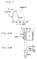
- Fig. 1 shows a graph of the collection efficiency ⁇ in relative amplitude of an amorphous silicon (a-Si) solar cell and that of a monocrystalline (mono-Si) solar cell plotted against the photon wavelength ⁇ in micrometer.
- the conversion efficiency is related to an area that the collection efficiency curve surrounds. As shown in Fig.
- the mono-Si curve extends up to a relatively long wavelength, whereas the a-Si curve is limited to a shorter wavelength. Therefore, the conversion efficiency of commercial amorphous silicon solar batteries is 7-8% which is rather lower than that of a monocrystalline silicon solar battery because the formers may not utilize solar energy as effectively as the latter does.
- a multi-layered solar battery which usually comprises semiconductor regions having different energy gaps.
- a region with the largest energy gap is positioned for it to absorb the incident light first, and the other regions are applied on the region further in series in order of the energy gap in order that the lower energy photons may penetrate deeper.
- Each region has its own peak value of the collection efficiency at a predetermined range of wavelength in the spectrum of solar light.
- This type of a device called a tandem solar battery, may raise the conversion efficiency because it utilizes the incident light more effectively than a solar cell made of one material does.
- a p-n junction is generally prepared by using junction formation methods including a high temperature process such as a thermal diffusion process or an annealing process after an ion implantation.
- the former is a process wherein impurities are diffused thermally into a crystalline semiconductor which is kept at a prescribed temperature as high as about 1000°C in an environment containing impurities to be doped.
- the latter is a process wherein ionized impurities to be doped are accelerated under high electric field so as to be implanted into a crystalline semiconductor.
- the width of the energy gap which affects the collection efficiency may be adjusted by selecting the kind and/or the mixing ratio of the gases supplied during a manufacturing process thereof.
- Hydrogenated amorphous silicon carbide, SiC:H, and/or hydrogenated amorphous silicon nitride, SiN:H have been used for shorter wavelength, while hydrogenated amorphous silicon germanide SiGe:H and/or hydrogenated amorphous silicon stannide SiSn:H have been used for longer wavelength.
- a hydrogenated amorphous semiconductors e.g., a-SiGe:H or a-SiSn:H
- a multi-layered amorphous solar battery comprising regions thereof cannot satisfactorily convert the light of longer wavelength to the photocurrent because of inferior photovoltaic properties of an amorphous solar cell.
- crystalline semiconductors e.g, Si, GaAs, or Ge
- having a narrow energy gap can utilize satisfactorily the light of longer wavelength.
- the reflection of the light incident on the surface of a solar cell is also important for its performance.
- An anti-reflecting transparent layer having a suitable refractive index and thickness has been applied on the surface of the outermost semiconductor region so as to minimize the reflection effectively.
- a heavily-doped tunnel junction or a transparent conductive layer has been inserted to provide an ohmic contact.
- an indium-tin-oxide transparent conductive layer is placed between a p-type crystalline silicon region and an n-type amorphous silicon region.
- US-A-4016586 concerns a photovoltaic device comprising an amorphous semiconductor region, e.g. of indium trioxide, applied on a crystalline semiconductor region, e.g. of silicon, with a p-n heterojunction formed between said regions and wherein said amorphous region is placed at the light receiving side so the said semiconductor regions are placed in the order of decreasing width of energy gap from the light receiving side.
- amorphous semiconductor region e.g. of indium trioxide
- crystalline semiconductor region e.g. of silicon
- an ohmic contact is provided at the interfaces between the unitary solar cells connected in series in a tandem solar cell without interposing any extra structure though a semiconductor region may be interposed if necessary as will be described below.
- an amorphous p-n junction may be formed between p-type and n-type amorphous regions by applying two unitary solar cells in series, and it provides an ohmic contact to the two unitary solar cells.
- Amorphous semiconductors have a unique characteristic that a high density of localized states exists in the forbidden band. Photogenerated electrons and holes are exchanged through those states at the amorphous p-n junction.
- the amorphous p-n junction serves to provide an ohmic contact between the unitary solar cells connected in series by utilizing the characteristic of an amorphous semiconductor. If such an amorphous p-n junction is not formed at the interface between the unitary cells, for example, between a crystalline and an amorphous solar cell, an amorphous semiconductor region will be intervened between the both so as to form an amorphous p-n junction providing an ohmic contact.
- Fig. 2(A) shows a schematic sectional view of an HJ solar cell which uses a p-type polycrystalline silicon wafer as a crystalline semiconducting material.
- An aluminum electrode 1 is evaporated onto the p-type wafer 2.
- An n-type thin film 3 of microcrystalline silicon is deposited on the opposite side of the p-type wafer 2 to the electrode 1 by the use of a glow discharged decomposition (GD) process.
- GD glow discharged decomposition
- an HJ solar cell comprises a p-type polycrystalline silicon wafer and an n-type microcrystalline silicon film which form a heterojunction (HJ).
- Fig. 2(B) shows the energy band diagram of the HJ solar cell, wherein E c , E v and E F represent the energy level at the bottom of the conduction band, the energy level at the top of the valence band and the Fermi level, respectively.
- the energy gap E ga that is, the width of the forbidden band, of the n-type microcrystalline silicon, which is about 1.8 eV, is greater than the energy gap E,gC of the p-type polycrystalline silicon which is about 1.1 ev.
- microcrystalline semiconductor 3 at the light-receiving side has a larger energy gap, photons with shorter wavelength cannot be absorbed in the microcrystalline semiconductor region 3 and are absorbed in the crystalline semiconductor region 2, which is the active region to generate mainly photocarriers. Consequently, this enhances the conversion of the solar energy into electric energy.
- I out and V out represent the output current, in terms of mA/cm2, and the output voltage of the solar cell, respectively.
- the conversion efficiency estimated from the I-V. characteristics shown in Fig 3 is about 11%. This value is generally of the same level as that of a solar cell which is manufactured from a polycrystalline silicon wafer by using a high temperature process such as a thermal diffusion process.
- n-type microcrystalline silicon can be deposited at a temperature between 200°C and 300°C, much lower than that used in the prior art high temperature process needed to form a p-n junction made of a crystalline silicon, for several minutes. Furthermore, this process is suitable to prepare devices having a large light-receiving area.
- an HJ solar ceil having the same level of performance as that of a solar cell manufactured by using a high temperature process, can be manufactured by using the low temperature process at low cost and in a continuous manufacturing process.
- a vacuum evaporation method an ion plating process, a sputtering method, or a photochemical vapor deposition process may be employed.
- materials such as crystalline GaAs and Ge can be substituted for the polycrystalline silicon 2, while others such as microcrystalline or amorphous, hydrogenated or fluoridated, SiC, SiN and SiGe can be substituted for the microcrystalline Si3, as far as E ga is larger then E gc .
- the types of conduction in the semiconductor regions may be reversed, so that a p-type amorphous or microcrystalline one 3 is applied on an n-type crystalline semiconductor region 2.
- Fig. 4 shows a schematic sectional view of an HJ solar cell wherein a crystalline semiconductor region 2′ is a thin film.
- a substrate 6 is a thin plate of inorganic solid such as metal, glass or ceramics, or a film of organic solid such as a polyimide.
- An electrode 1′ applied on the substrate 6 forms an ohmic contact with a p-type crystalline thin film 2′, which is further deposited thereon by using such a process as a chemical vapor deposition (CVD) process, a metal-organic CVD (MOCVD) process, a molecular beam epitaxy (MBE) process, a sputtering process or an ion plating process.
- CVD chemical vapor deposition
- MOCVD metal-organic CVD
- MBE molecular beam epitaxy
- the n-type microcrystalline or amorphous silicon thin film 3 is deposited onto the crystalline semiconductor 2′ by using the GD process.
- the transparent conductive film 4 and the comb-like electrode 5 are applied on the thin film 3 in succession.
- the substrate 6 consists of a metallic material, it serves also as an ohmic electrode and it may not be necessary to use the electrode 1′ separately.
- the crystalline semiconductor 2′ as well as the region 3 are prepared by using the thin film process so that the manufacturing cost of the solar cell can be lowered further than that of the first example.
- a crystalline film 2′ is made of expensive materials such as GaAs and Ge, which can absorb sunlight in the form of thin films less than several micrometer, it may be more effective to provide a solar cell of high performance at a lower cost. If such a process as the CVD and MOCVD process which are suitable for forming a large-area film is adopted to deposit a crystalline semiconductor 2′, a device having a large light-receiving area may be manufactured.
- Fig. 5(A) shows a photovoltaic device according to a first embodiment of the present invention wherein an HJ solar cell C and an amorphous solar cell A are connected in series.
- the first solar cell C comprises a p-type wafer 2 of polycrystalline silicon and an n-type region 3 of amorphous or microcrystalline silicon which form an HJ
- the second cell A comprises a p-type region 21, an i-type region 22, and an n-type region 23 of amorphous or microcrystalline silicon which form a p-i-n junction.
- An aluminum electrode 1 is deposited on the p-type semiconductor 2, while a transparent conductive film 4 of ITO and an comblike electrode 5 is applied in succession on the n-type semiconductor 23.
- the thicknesses of those amorphous regions and ITO 3, 21, 22, 23 and 4 are about 300, 50, 500, 10 and 70 nm (3000, 500, 5000, 100 and 700 ⁇ ) respectively. It should be noted that the crystalline film may be substituted for a crystalline wafer 2; a substrate as used in fig.4 is needed in case of such a substitution. It should also be noted that the type of conduction in the semiconductor regions may be reversed.
- Fig. 5(B) shows a schematic energy band diagram of the photovoltaic device shown in Fig. 5(A).
- An energy gap E gc of the p-type polycrystalline silicon 2, about 1.1 eV, is smaller than that E ga of the i-type amorphous layer 22 which mainly generates photocarriers in the second cell A, about 1.7-1.8 eV.
- the first embodiment of the present invention is characterized in that an ohmic contact is realized easily at an amorphous p-n junction by the use of a unique characteristic of an amorphous semiconductor that many localized states exist in the forbidden band, though the characteristic is disadvantageous in most cases.
- the absorption of light creates electron-hole pairs as shown in Fig. 5(B).
- the amorphous p-n junction serves as an ohmic junction (OJ).
- Fig. 6 is a graph showing the collection efficiency ⁇ of the amorphous silicon solar cell C (a-Si) and of the H-J solar cell (poly-Si) shown in Fig. 2(A), covered with a filter of amorphous silicon having a thickness of 600 nm (6000 ⁇ ), plotted against the wavelength ⁇ of the incident light.
- the latter data poly-Si can be considered to be almost equal to the collection efficiency of the HJ solar cell C composing the tandem solar cell shown in Fig. 5(A).
- the spectrum curve of the solar energy is shown for reference as the chain line Sun-S in relative amplitude. Since the photovoltaic device shown in Fig. 5(A) comprises two types of materials with different light-sensitivity, as shown in Fig.
- Fig. 7 shows the data of I-V characteristics of the photovoltaic device shown in Fig. 5(A).
- the conversion efficiency obtained from the data is 11-12%, which is higher than that exhibited by the prior art amorphous solar cells, i.e., 7 to 8% in general.
- Fig. 8(A) is a schematic sectional view of a photovoltaic device according to a second embodiment of the present invention.
- Two amorphous solar cells A1 and A2 are formed by depositing amorphous materials successively by means of the GD process on an HJ solar cell C described with reference to Fig. 2 to result in a tandem solar battery.
- the three unitary cells are connected in series.
- a substrate 2 is made of a thin plate of inorganic material such as metal, glass or ceramics, or of a film of organic solid such as a polyimide.
- An ohmic electrode 1 is deposited on the substrate 2, and a p-type crystalline 41 and an n-type amorphous region 42 are deposited further in succession to form a crystalline cell C.
- a p-type region 21, an i-type region 22 and an n-type region 23 of amorphous silicon are deposited on the n-type region 42 to form a second cell Al.
- a p-type region 31, an i-type region 32 and an n-type region 33 of amorphous silicon carbide are deposited on the n-type amorphous silicon 22 in succession to form a third cell A2.
- the junctions between the cells comprising a p-type and an n-type amorphous material provide an ohmic contact.
- a transparent conductive film 4 of ITO and a comb-like electrode 5 are deposited in succession on the semiconductor 33. It should be noted that a crystalline wafer may be substituted for a crystalline thin film 41 in the cell C; the substrate 2 is needless in case of such a substitution. It should also be noted that the type of conduction in the semiconductor regions may be reversed.
- Fig. 8(B) shows a schematic energy band diagram of the photovoltaic device shown in Fig. 8(A), wherein the energy gap E gc of the crystalline GaAs in the cell C is about 1.4 eV, the energy gap E ga1 of the i-type amorphous silicon 22 in the first amorphous cell A1 larger than E gc is about 1.8 eV, and the energy gap E ga2 of the i-type amorphous silicon carbide 32 larger than E ga1 is about 2.0 eV.
- the incident light first enters the cell A2 with the largest energy gap E ga2 , and light of shorter wavelength is absorbed thereby; the light transmitted through the cell A2 is absorbed in the next cell A1 with the energy gap E ga1 ; finally, the light of longer wavelength transmitted through the cell A1 is absorbed in the cell C with the smallest energy gap E gc .
- solar energy of shorter wavelength may be absorbed in the amorphous solar cells A1 and A2 with p-i-n junctions, and that of longer wavelength may be absorbed by the HJ solar cell C with a p-n HJ. Then, high conversion efficiency of a solar battery can be realized.
- Fig. 9(A) shows a schematic sectional view of a photovoltaic device according to a third embodiment of the present invention.
- a tandem solar battery is constructed from two HJ solar cells C1 and C2 connected together in series with the intervention of an amorphous semiconductor region 11 whose type of conduction is controlled to have the same sign as those in a crystalline semiconductor region 12 to provide an ohmic contact between them.
- a solar cell C1 similar to that in Fig. 2(A), comprises a p-type crystalline semiconductor wafer 2 with an energy gape E gc1 and an n-type microcrystalline or amorphous layer 3 with an energy gap E ga1 larger than E gc1 ; both layers 2 and 3 form a p-n HJ.
- the wafer 2 may be substituted for by a crystalline semiconductor thin film.
- the p-type amorphous layer 11 is deposited on the amorphous layer 3.
- the p-type crystalline semiconductor 12 having an energy gap E gc2 larger than E gc1 and an n-type amorphous crystalline semiconductor 13 having an energy gap E ga2 larger than E gc2 are deposited on the semiconductor 11 in succession.
- the second solar cell C2 comprises the semiconductor regions 12 and 13 which form a p-n HJ.
- solar energy of shorter wavelength is absorbed in the solar cell C2 with a larger energy gap adjoining to the transparent electrode 4, and then solar energy with longer wavelength may be absorbed in the solar cell C1 with a narrower gap. Then, a high conversion efficiency solar battery may be realized at a low manufacturing cost.
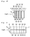
- Fig. 10 shows a schematic sectional view of a photovoltaic device of the fourth embodiment according to a present invention. It is constructed by connecting the two HJ solar cells C1 and C2 and the two amorphous solar cells A1 and A2 in series.
- numerals 1 to 5 and 11 to 13 represent like parts shown in Fig. 9(A)
- numerals 21 to 23 and 31 to 33 represent like parts shown in Fig. 8(A).
- Fig. 11 shows schematically another photovoltaic device. It comprises six cells connected in series. Three of them are HJ solar cells C1 to C3, and the others are amorphous cells A1 to A3. These cells are connected in series and are applied on a stainless steel substrate 1 with the heterojunction formed around the interface between cells C3 and A1.
- the stainless steel substrate 1 serves also as an electrode.
- the transparent conductive layer 4 and the comb-like electrode 5 are applied in succession on the cell A3.
- the crystalline semiconductor regions in the three HJ cells C1, C2 and C3 are made from germanium, silicon and GaAs, respectively, and the energy gap E gc1 , E gc2 and E gc3 in the crystalline region are 0.7, 1.1 and 1.4eV, respectively.
- the three amorphous cells A1, A2 and A3 are made from amorphous silicon germanide, amorphous silicon and amorphous silicon carbide, respectively, and the energy gap E ga1 , E ga2 and E ga3 are 1.6, 1.8 and 2.0 eV, respectively.
- Ohmic contacts are provided at the interfaces between the cells.
- Light of shorter wavelength is absorbed in the third amorphous cell A3 with the largest energy gap E ga3 situated adjoining to the light-receiving surface 4 through which the light enters.
- the light transmits through the cells applied in one another in series in the order of the energy gap, the light is absorbed successively from at shorter wavelength to at longer wavelength.
- light in a wide range may be utilized in a single device.
- Fig. 12(A) shows a schematic model of a crystalline wafer 2 having an irregular surface designed so as to increase the absorption of the incident light.
- a number of small pyramid-shaped protrusions are formed on the surface of a crystalline semiconductor wafer 2 or of a thin plate made of an inorganic or organic solid.
- a photovoltaic cell according to all the embodiments of the present invention may be manufactured by depositing materials on a substrate of this type.
- a part of the photovoltaic device in the third embodiment manufactured by successive deposition on the substrate shown in Fig. 12(A) is shown in sectional representation in Fig. 12(B) wherein 4 designates a transparent conductive film, A an amorphous solar cell and C an H-J solar cell.
- An incident light transmitted through the conductive layer 4 is reflected partially at the interface between the transparent conductive layer 4 and the amorphous region 21, and between the semiconductors 2 and 3.
- the solid line in Fig. 12(B) indicates the confinement of light in the semiconductor layer 2.
- the confinement effect caused by the multiple reflection may increase the conversion efficiency by enhancing the absorption of the incident light.
- a photovoltaic device having tandem structure disclosed in the first to fourth embodiments can be used not only as a solar cell but also as a photodetector by using the different photosensitivities of unitary cells composing the photovoltaic device.
Description
- The present invention relates to a photovoltaic device applicable as a solar battery, a photodetector or the like. More particularly, it relates to a photovoltaic device known as a tandem solar battery wherein solar energy is absorbed in several regions having different energy gaps.
- A solar cell is a photovoltaic device comprising p-type and n-type materials and having a p-n junction at the interface between them for the conversion of solar energy directly to electrical energy. A solar battery usually consists of a plurality of solar cells connected in series and parallel to each other in a matrix fashion where a large power output is required. Hitherto, commercial solar batteries comprising a p-n, homo-, or heterojunction of monocrystalline or polycrystalline Si, GaAs, CdS, CdTe or the like are available as well as those comprising a p-type, an i-type and an n-type layer of amorphous silicon each deposited in series and forming a p-i-n junction. Moreover, it has been suggested that a solar battery comprising a plurality of solar cells, each of which has a p-type, an i-type and an n-type amorphous silicon layer each deposited in series, which battery may produce a high output voltage.
- In the disclosure herein described, the following terms are to be construed as having the following meanings. The term "heterojunction (HJ)" is a junction formed between semiconductor regions made of different materials. The term "junction" is homojunction made of the same material as is often used as including heterojunction. The "p-n junction" is a region of transition between p-type and n-type semiconductor regions. The term "p-in junction" is a region of successive transition between a p-type and an i-type semiconductor region and between the i-type and an n-type semiconductor region. In the field of solar cells, it is only used for solar cells made from amorphous material and plays the same role as the p-n junction in a solar cell made of crystalline material as for the photogeneration of carriers. The term "amorphous p-n junction" is a region of transition formed between p-type and n-type amorphous semiconductor regions, and provides an ohmic contact between the two regions. The term "unitary cell" is sometimes used to name a solar cell which constitute a tandem solar battery. A crystalline solar cell is a solar cell wherein a p-n junction is formed from crystalline regions. An amorphous solar cell is a solar cell wherein a p-i-n junction is formed from amorphous materials. A heterojunction (HJ) solar cell is a solar cell comprising a crystalline region and an amorphous region and having a p-n heterojunction between them. The adjective "amorphous" is often used as including a microcrystalline structure because a microcrystalline semiconductor may be substituted for an amorphous semiconductor in many cases.
- Economical solar batteries are necessary for them to be widely utilized in practice. It has generally been considered that a thin-film process may lower the manufacturing cost of a solar battery. In this respect, a manufacturing process using amorphous silicon is considered desirable because it may reduce the thickness of an amorphous semiconductor region down to the order of 0.5 micrometer in contrast to about 300 micrometer in thickness of a monocrystalline silicon region which is generally employed in a crystalline or HJ solar cell. It has been expected that a thin-film process may produce a large-area device having a large light-receiving area.
- The efficiency to convert solar energy into electric energy is closely related to the manufacturing cost of a photovoltaic device. An amorphous silicon solar battery has a disadvantage of having the conversion efficiency lower than that of a monocrystalline silicon solar battery, though the amorphous silicon solar battery is expected to lower the manufacturing cost when a thin film process is used to make it. Fig. 1 shows a graph of the collection efficiency η in relative amplitude of an amorphous silicon (a-Si) solar cell and that of a monocrystalline (mono-Si) solar cell plotted against the photon wavelength λ in micrometer. The conversion efficiency is related to an area that the collection efficiency curve surrounds. As shown in Fig. 1, the mono-Si curve extends up to a relatively long wavelength, whereas the a-Si curve is limited to a shorter wavelength. Therefore, the conversion efficiency of commercial amorphous silicon solar batteries is 7-8% which is rather lower than that of a monocrystalline silicon solar battery because the formers may not utilize solar energy as effectively as the latter does.
- In order to improve the conversion efficiency of a solar battery, a multi-layered solar battery has been studied which usually comprises semiconductor regions having different energy gaps. A region with the largest energy gap is positioned for it to absorb the incident light first, and the other regions are applied on the region further in series in order of the energy gap in order that the lower energy photons may penetrate deeper. Each region has its own peak value of the collection efficiency at a predetermined range of wavelength in the spectrum of solar light. This type of a device, called a tandem solar battery, may raise the conversion efficiency because it utilizes the incident light more effectively than a solar cell made of one material does.
- As for the manufacturing process, it is desirable to adopt a low temperature process. In crystalline solar cells, a p-n junction is generally prepared by using junction formation methods including a high temperature process such as a thermal diffusion process or an annealing process after an ion implantation. The former is a process wherein impurities are diffused thermally into a crystalline semiconductor which is kept at a prescribed temperature as high as about 1000°C in an environment containing impurities to be doped. The latter is a process wherein ionized impurities to be doped are accelerated under high electric field so as to be implanted into a crystalline semiconductor. In the ion implantation process, it is necessary to anneal the implanted semiconductor at a temperature as high as about 1000°C because the crystal structure has been disordered largely when the ions has been implanted. On the other hand, a high temperature process requires a complex set-up and careful control in operation, and this increases the manufacturing cost of a solar battery. In addition, it lowers the conversion efficiency of the solar battery because undesirable impurities migrate into the crystalline semiconductor from surroundings.
- With respect to an amorphous solar cell, the width of the energy gap which affects the collection efficiency may be adjusted by selecting the kind and/or the mixing ratio of the gases supplied during a manufacturing process thereof. Hydrogenated amorphous silicon carbide, SiC:H, and/or hydrogenated amorphous silicon nitride, SiN:H, have been used for shorter wavelength, while hydrogenated amorphous silicon germanide SiGe:H and/or hydrogenated amorphous silicon stannide SiSn:H have been used for longer wavelength. However, though a hydrogenated amorphous semiconductors (e.g., a-SiGe:H or a-SiSn:H) having a narrow energy gap can absorb light of longer wavelength, a multi-layered amorphous solar battery comprising regions thereof cannot satisfactorily convert the light of longer wavelength to the photocurrent because of inferior photovoltaic properties of an amorphous solar cell. On the contrary, crystalline semiconductors (e.g, Si, GaAs, or Ge) having a narrow energy gap can utilize satisfactorily the light of longer wavelength.
- The reflection of the light incident on the surface of a solar cell is also important for its performance. An anti-reflecting transparent layer having a suitable refractive index and thickness has been applied on the surface of the outermost semiconductor region so as to minimize the reflection effectively.
- In tandem solar batteries, it is necessary for the interface between unitary cells to provide a contact which does not bring about an electrical and optical loss in performance of a solar battery. A heavily-doped tunnel junction or a transparent conductive layer has been inserted to provide an ohmic contact. For example, in US-A-4,292,461, an indium-tin-oxide transparent conductive layer is placed between a p-type crystalline silicon region and an n-type amorphous silicon region.
- It should be noted, however, that the addition of such an extra material as indium-tin-oxide is liable to lead to deterioration of an amorphous solar cell because of undesirable impurities such as indium atoms or oxygen atoms migrating in the amorphous region during the deposition.
- US-A-4016586 concerns a photovoltaic device comprising an amorphous semiconductor region, e.g. of indium trioxide, applied on a crystalline semiconductor region, e.g. of silicon, with a p-n heterojunction formed between said regions and wherein said amorphous region is placed at the light receiving side so the said semiconductor regions are placed in the order of decreasing width of energy gap from the light receiving side.
- From US-A-42 53 882 a photovoltaic device is known which shows two semiconductor cells forming a heterojunction and being formed from crystalline semiconductor and an amorphous semiconductor respectively.
- It is an object of the present invention to provide a high-efficiency photovoltaic device by using a tandem structure comprising at least one crystalline semiconductor region and one amorphous semiconductor region, wherein the two regions are applied on each other without interposing any extra structure in the photo-generating regions.
- It is another object of the present invention to provide a high-efficiency photovoltaic device by using a tandem structure by applying a plurality of unitary cells, in order to improve the conversion efficiency and without interposing any extra structure in the photogenerating regions, though an amorphous semiconductor region may be interposed if necessary as will be described below.
- In accordance with the present invention, an ohmic contact is provided at the interfaces between the unitary solar cells connected in series in a tandem solar cell without interposing any extra structure though a semiconductor region may be interposed if necessary as will be described below. In other words, an amorphous p-n junction may be formed between p-type and n-type amorphous regions by applying two unitary solar cells in series, and it provides an ohmic contact to the two unitary solar cells. Amorphous semiconductors have a unique characteristic that a high density of localized states exists in the forbidden band. Photogenerated electrons and holes are exchanged through those states at the amorphous p-n junction. Therefore, the amorphous p-n junction serves to provide an ohmic contact between the unitary solar cells connected in series by utilizing the characteristic of an amorphous semiconductor. If such an amorphous p-n junction is not formed at the interface between the unitary cells, for example, between a crystalline and an amorphous solar cell, an amorphous semiconductor region will be intervened between the both so as to form an amorphous p-n junction providing an ohmic contact.
- The object of the invention is met by the features of the
claims -
- Fig. 1 is a graph showing the collection efficiency η of both of a monocrystalline silicon (mono-Si) solar cell and of an amorphous silicon (a-Si) solar cell plotted against the photon wavelength λ;
- Fig. 2A is a schematic sectional view of a solar cell;
- Fig. 2(B) is an energy band diagram of a solar cell shown in Fig. 2(A);
- Fig. 3 is a graph showing the I-V characteristics of a solar cell shown in Fig. 2(A);
- Fig. 4 is a schematic sectional view of a photovoltaic device;
- Fig. 5(A) is a schematic sectional view of a photovoltaic device according to a first embodiment of the present invention;
- Fig. 5(B) is a schematic energy band diagram of a photovoltaic device shown in Fig. 5(A);
- Fig. 6 is a graph showing the collection efficiency η of an amorphous silicon solar cell (a-Si) and of the HJ solar cell (poly-Si) shown in Fig. 2(A), covered with a filter of an amorphous silicon having a thickness of 600 nm (6000 Å), plotted against the wavelength λ of the incident light;
- Fig. 7 is a graph of the i-V characteristics of a photovoltaic device shown in Fig. 5(A); Fig. 8(A) is a schematic sectional view of a photovoltaic device according to a second embodiment of the present invention;
- Fig. 8(B) is a schematic energy band diagram of a solar battery shown in Fig. 8(A); Fig. 9(A) is a schematic sectional view of a photovoltaic device according to a third embodiment of the present invention;
- Fig. 9(B) is an energy band diagram of a solar battery shown in Fig. 9(A) across the p-n junction;
- Fig. 10 is a schematic sectional view of a photovoltaic device according to a fourth embodiment of the present invention;
- Fig. 11 is a schematic sectional view of a photovoltaic device according to a fifth embodiment of the present invention;
- Fig. 12(A) is a perspective view, on an enlarged scale, of substrate having an irregular surface; and
- Fig. 12(B) is a schematic sectional view of a solar cell manufactured by the use of the substrate shown in Fig. 12(A).
- Referring now to the drawings, wherein like reference characters designate like parts throughout the several views thereof, Fig. 2(A) shows a schematic sectional view of an HJ solar cell which uses a p-type polycrystalline silicon wafer as a crystalline semiconducting material. An
aluminum electrode 1 is evaporated onto the p-type wafer 2. An n-typethin film 3 of microcrystalline silicon is deposited on the opposite side of the p-type wafer 2 to theelectrode 1 by the use of a glow discharged decomposition (GD) process. A transparentconductive film 4 of indium-tin-oxide (ITO) which acts as both the front electrode and an antireflectance layer is further applied on the n-type semiconductor region 3, and a comb-like aluminum electrode 5 is still further applied on thetransparent layer 4, through which solar energy is transmitted into both semiconductor regions in operation. Theelectrodes - Fig. 2(B) shows the energy band diagram of the HJ solar cell, wherein Ec, Ev and EF represent the energy level at the bottom of the conduction band, the energy level at the top of the valence band and the Fermi level, respectively. The energy gap Ega, that is, the width of the forbidden band, of the n-type microcrystalline silicon, which is about 1.8 eV, is greater than the energy gap E,gC of the p-type polycrystalline silicon which is about 1.1 ev. Since the
microcrystalline semiconductor 3 at the light-receiving side has a larger energy gap, photons with shorter wavelength cannot be absorbed in themicrocrystalline semiconductor region 3 and are absorbed in thecrystalline semiconductor region 2, which is the active region to generate mainly photocarriers. Consequently, this enhances the conversion of the solar energy into electric energy. - Experimental data on the I-V characteristics of the solar cell is shown in Fig. 3, where Iout and Vout represent the output current, in terms of mA/cm², and the output voltage of the solar cell, respectively. The conversion efficiency estimated from the I-V. characteristics shown in Fig 3 is about 11%. This value is generally of the same level as that of a solar cell which is manufactured from a polycrystalline silicon wafer by using a high temperature process such as a thermal diffusion process.
- In the GD process, materials which contain constituent atoms of the film to be obtained and which are transformed into the plasma state, are decomposed into chemically active ions and/or radicals to form films at low temperatures. By the use of the GD process, n-type microcrystalline silicon can be deposited at a temperature between 200°C and 300°C, much lower than that used in the prior art high temperature process needed to form a p-n junction made of a crystalline silicon, for several minutes. Furthermore, this process is suitable to prepare devices having a large light-receiving area. Thus, an HJ solar ceil having the same level of performance as that of a solar cell manufactured by using a high temperature process, can be manufactured by using the low temperature process at low cost and in a continuous manufacturing process.
- Alternatively, other low temperature processes than the GD process may be used to deposit the
amorphous semiconductor 3 on thesubstrate 2. For example, a vacuum evaporation method, an ion plating process, a sputtering method, or a photochemical vapor deposition process may be employed. - It should be noted that materials such as crystalline GaAs and Ge can be substituted for the
polycrystalline silicon 2, while others such as microcrystalline or amorphous, hydrogenated or fluoridated, SiC, SiN and SiGe can be substituted for the microcrystalline Si3, as far as Ega is larger then Egc. The types of conduction in the semiconductor regions may be reversed, so that a p-type amorphous ormicrocrystalline one 3 is applied on an n-typecrystalline semiconductor region 2. - Fig. 4 shows a schematic sectional view of an HJ solar cell wherein a
crystalline semiconductor region 2′ is a thin film. Asubstrate 6 is a thin plate of inorganic solid such as metal, glass or ceramics, or a film of organic solid such as a polyimide. Anelectrode 1′ applied on thesubstrate 6 forms an ohmic contact with a p-type crystallinethin film 2′, which is further deposited thereon by using such a process as a chemical vapor deposition (CVD) process, a metal-organic CVD (MOCVD) process, a molecular beam epitaxy (MBE) process, a sputtering process or an ion plating process. The n-type microcrystalline or amorphous siliconthin film 3 is deposited onto thecrystalline semiconductor 2′ by using the GD process. The transparentconductive film 4 and the comb-like electrode 5 are applied on thethin film 3 in succession. If thesubstrate 6 consists of a metallic material, it serves also as an ohmic electrode and it may not be necessary to use theelectrode 1′ separately. - In this HJ solar cell the
crystalline semiconductor 2′ as well as theregion 3 are prepared by using the thin film process so that the manufacturing cost of the solar cell can be lowered further than that of the first example. Especially, if acrystalline film 2′ is made of expensive materials such as GaAs and Ge, which can absorb sunlight in the form of thin films less than several micrometer, it may be more effective to provide a solar cell of high performance at a lower cost. If such a process as the CVD and MOCVD process which are suitable for forming a large-area film is adopted to deposit acrystalline semiconductor 2′, a device having a large light-receiving area may be manufactured. - Fig. 5(A) shows a photovoltaic device according to a first embodiment of the present invention wherein an HJ solar cell C and an amorphous solar cell A are connected in series. The first solar cell C comprises a p-
type wafer 2 of polycrystalline silicon and an n-type region 3 of amorphous or microcrystalline silicon which form an HJ, while the second cell A comprises a p-type region 21, an i-type region 22, and an n-type region 23 of amorphous or microcrystalline silicon which form a p-i-n junction. Analuminum electrode 1 is deposited on the p-type semiconductor 2, while a transparentconductive film 4 of ITO and ancomblike electrode 5 is applied in succession on the n-type semiconductor 23. The thicknesses of those amorphous regions andITO crystalline wafer 2; a substrate as used in fig.4 is needed in case of such a substitution. It should also be noted that the type of conduction in the semiconductor regions may be reversed. - Fig. 5(B) shows a schematic energy band diagram of the photovoltaic device shown in Fig. 5(A). An energy gap Egc of the p-
type polycrystalline silicon 2, about 1.1 eV, is smaller than that Ega of the i-typeamorphous layer 22 which mainly generates photocarriers in the second cell A, about 1.7-1.8 eV. - In order to connect the unitary solar cells in series effectively in a tandem structure, it is necessary to provide an ohmic contact at the interfaces between the unitary solar cells. The first embodiment of the present invention is characterized in that an ohmic contact is realized easily at an amorphous p-n junction by the use of a unique characteristic of an amorphous semiconductor that many localized states exist in the forbidden band, though the characteristic is disadvantageous in most cases. The absorption of light creates electron-hole pairs as shown in Fig. 5(B). Holes h in the amorphous solar cell A and electrons e in the H-J solar cell C created by the absorption of solar energy recombine through localized states Es in the forbidden band at the interface between the two unitary cells, that is, a recombination current flows across the interface, so that an ohmic contact is provided between the two solar cells. The amorphous p-n junction serves as an ohmic junction (OJ).
- Fig. 6 is a graph showing the collection efficiency η of the amorphous silicon solar cell C (a-Si) and of the H-J solar cell (poly-Si) shown in Fig. 2(A), covered with a filter of amorphous silicon having a thickness of 600 nm (6000 Å), plotted against the wavelength λ of the incident light. The latter data poly-Si can be considered to be almost equal to the collection efficiency of the HJ solar cell C composing the tandem solar cell shown in Fig. 5(A). The spectrum curve of the solar energy is shown for reference as the chain line Sun-S in relative amplitude. Since the photovoltaic device shown in Fig. 5(A) comprises two types of materials with different light-sensitivity, as shown in Fig. 6, it may absorb solar energy in a wide range of wavelength effectively and increases the conversion efficiency of the device. Fig. 7 shows the data of I-V characteristics of the photovoltaic device shown in Fig. 5(A). The conversion efficiency obtained from the data is 11-12%, which is higher than that exhibited by the prior art amorphous solar cells, i.e., 7 to 8% in general.
- The efficiency value of 11-12% has been obtained in an early stage of our study. By optimizing amorphous silicon layers, the conversion efficiency of more than 15% will probably be attained in this type of cell. Moreover, though a polycrystalline silicon wafer as a crystalline material is used in this embodiment, a thin film of other materials such as GaAs, Ge and Si can be substituted for the polycrystalline silicon wafer so that the manufacturing cost of a solar cell may be reduced further.
- Fig. 8(A) is a schematic sectional view of a photovoltaic device according to a second embodiment of the present invention. Two amorphous solar cells A1 and A2 are formed by depositing amorphous materials successively by means of the GD process on an HJ solar cell C described with reference to Fig. 2 to result in a tandem solar battery. The three unitary cells are connected in series. A
substrate 2 is made of a thin plate of inorganic material such as metal, glass or ceramics, or of a film of organic solid such as a polyimide. Anohmic electrode 1 is deposited on thesubstrate 2, and a p-type crystalline 41 and an n-type amorphous region 42 are deposited further in succession to form a crystalline cell C. A p-type region 21, an i-type region 22 and an n-type region 23 of amorphous silicon are deposited on the n-type region 42 to form a second cell Al. A p-type region 31, an i-type region 32 and an n-type region 33 of amorphous silicon carbide are deposited on the n-typeamorphous silicon 22 in succession to form a third cell A2. The junctions between the cells comprising a p-type and an n-type amorphous material provide an ohmic contact. Finally, a transparentconductive film 4 of ITO and a comb-like electrode 5 are deposited in succession on thesemiconductor 33. It should be noted that a crystalline wafer may be substituted for a crystalline thin film 41 in the cell C; thesubstrate 2 is needless in case of such a substitution. It should also be noted that the type of conduction in the semiconductor regions may be reversed. - Fig. 8(B) shows a schematic energy band diagram of the photovoltaic device shown in Fig. 8(A), wherein the energy gap Egc of the crystalline GaAs in the cell C is about 1.4 eV, the energy gap Ega1 of the i-type
amorphous silicon 22 in the first amorphous cell A1 larger than Egc is about 1.8 eV, and the energy gap Ega2 of the i-typeamorphous silicon carbide 32 larger than Ega1 is about 2.0 eV. The incident light first enters the cell A2 with the largest energy gap Ega2, and light of shorter wavelength is absorbed thereby; the light transmitted through the cell A2 is absorbed in the next cell A1 with the energy gap Ega1; finally, the light of longer wavelength transmitted through the cell A1 is absorbed in the cell C with the smallest energy gap Egc. Thus, in the device shown in Fig. 8(A), solar energy of shorter wavelength may be absorbed in the amorphous solar cells A1 and A2 with p-i-n junctions, and that of longer wavelength may be absorbed by the HJ solar cell C with a p-n HJ. Then, high conversion efficiency of a solar battery can be realized. - Fig. 9(A) shows a schematic sectional view of a photovoltaic device according to a third embodiment of the present invention. A tandem solar battery is constructed from two HJ solar cells C1 and C2 connected together in series with the intervention of an amorphous semiconductor region 11 whose type of conduction is controlled to have the same sign as those in a
crystalline semiconductor region 12 to provide an ohmic contact between them. A solar cell C1, similar to that in Fig. 2(A), comprises a p-typecrystalline semiconductor wafer 2 with an energy gape Egc1 and an n-type microcrystalline oramorphous layer 3 with an energy gap Ega1 larger than Egc1; bothlayers wafer 2 may be substituted for by a crystalline semiconductor thin film. The p-type amorphous layer 11 is deposited on theamorphous layer 3. Then, the p-type crystalline semiconductor 12 having an energy gap Egc2 larger than Egc1 and an n-typeamorphous crystalline semiconductor 13 having an energy gap Ega2 larger than Egc2 are deposited on the semiconductor 11 in succession. The second solar cell C2 comprises thesemiconductor regions amorphous semiconductor 3. In the third embodiment, solar energy of shorter wavelength is absorbed in the solar cell C2 with a larger energy gap adjoining to thetransparent electrode 4, and then solar energy with longer wavelength may be absorbed in the solar cell C1 with a narrower gap. Then, a high conversion efficiency solar battery may be realized at a low manufacturing cost. - Fig. 10 shows a schematic sectional view of a photovoltaic device of the fourth embodiment according to a present invention. It is constructed by connecting the two HJ solar cells C1 and C2 and the two amorphous solar cells A1 and A2 in series. In the Fig. 10,
numerals 1 to 5 and 11 to 13 represent like parts shown in Fig. 9(A), andnumerals 21 to 23 and 31 to 33 represent like parts shown in Fig. 8(A). Solar energy is absorbed successively first in an amorphous solar cell A2 with an energy gap Ega2, then in another amorphous one A1 with an energy gap Ega1 narrower than Ega2, in an HJ solar cell C2 with an energy gap Egc2 narrower than Ega1, and finally in the HJ solar cell C1 with an energy gap Egc1 narrower than Egc2. Therefore, high conversion efficiency of a solar battery can be manufactured at a low cost. - Fig. 11 shows schematically another photovoltaic device. It comprises six cells connected in series. Three of them are HJ solar cells C1 to C3, and the others are amorphous cells A1 to A3. These cells are connected in series and are applied on a
stainless steel substrate 1 with the heterojunction formed around the interface between cells C3 and A1. Thestainless steel substrate 1 serves also as an electrode. The transparentconductive layer 4 and the comb-like electrode 5 are applied in succession on the cell A3. The crystalline semiconductor regions in the three HJ cells C1, C2 and C3 are made from germanium, silicon and GaAs, respectively, and the energy gap Egc1, Egc2 and Egc3 in the crystalline region are 0.7, 1.1 and 1.4eV, respectively. On the other hand, the three amorphous cells A1, A2 and A3 are made from amorphous silicon germanide, amorphous silicon and amorphous silicon carbide, respectively, and the energy gap Ega1, Ega2 and Ega3 are 1.6, 1.8 and 2.0 eV, respectively. Ohmic contacts are provided at the interfaces between the cells. Light of shorter wavelength is absorbed in the third amorphous cell A3 with the largest energy gap Ega3 situated adjoining to the light-receivingsurface 4 through which the light enters. As the light transmits through the cells applied in one another in series in the order of the energy gap, the light is absorbed successively from at shorter wavelength to at longer wavelength. Thus, light in a wide range may be utilized in a single device. - Fig. 12(A) shows a schematic model of a
crystalline wafer 2 having an irregular surface designed so as to increase the absorption of the incident light. A number of small pyramid-shaped protrusions are formed on the surface of acrystalline semiconductor wafer 2 or of a thin plate made of an inorganic or organic solid. A photovoltaic cell according to all the embodiments of the present invention may be manufactured by depositing materials on a substrate of this type. A part of the photovoltaic device in the third embodiment manufactured by successive deposition on the substrate shown in Fig. 12(A) is shown in sectional representation in Fig. 12(B) wherein 4 designates a transparent conductive film, A an amorphous solar cell and C an H-J solar cell. An incident light transmitted through theconductive layer 4 is reflected partially at the interface between the transparentconductive layer 4 and theamorphous region 21, and between thesemiconductors semiconductor layer 2. The confinement effect caused by the multiple reflection may increase the conversion efficiency by enhancing the absorption of the incident light. - It should be noted that a photovoltaic device having tandem structure disclosed in the first to fourth embodiments can be used not only as a solar cell but also as a photodetector by using the different photosensitivities of unitary cells composing the photovoltaic device.
Claims (10)
- A photovoltaic device which converts solar energy to electric energy, comprising, in combination, a p-n hetero-junction solar cell (C), including a crystalline semiconductor region (2) and an amorphous or microcrystalline Si, SiC, SiN or SiGe-region (3) which is placed toward the light receiving side of the device and applied on said crystalline region with a p-n heterojunction (HJ) formed between said regions, and an amorphous solar cell (A) applied on said hetero-junction solar cell (C) in series, and including a p-type region (21), an i-type region (22) and a n-type region (23) of amorphous or microcrystalline semiconductor applied in series so as to form a p-i-n junction, a p-n junction (OJ) providing an ohmic contact being formed at the interface between the amorphous or microcrystalline Si, SiC, SiN or SiGe region (3) of said p-n heterojunction solar cell and said adjoining amorphous solar cell, wherein said semiconductor regions are placed in the order of decreasing width of the energy gap from the light receiving side.
- The device according to claim 1, wherein said crystalline semiconductor region (2) in said heterojunction solar cell is a wafer.
- The device according to claim 1, wherein said crystalline semiconductor region in said hetero-junction solar cell is a thin film deposited on a substrate of inorganic material or organic material.
- The device according to claim 3, wherein said substrate has an irregular surface.
- A photovoltaic device which converts solar energy to electric energy, comprising, in combination, a p-n hetero-junction solar cell (C), including a crystalline semiconductor region (41) and an amorphous Si, SiC, SiN or SiGe-region (42), which is placed toward the light receiving side of the device and applied on said crystalline region with a p-n heterojunction (HJ) formed between said regions, and two amorphous solar cells (A₁, A₂) in series, and each including a p-type region (21, 31), an i-type region (22, 32) and an n-type region (23, 33) of amorphous or microcrystalline semiconductor regions applied in series so as to form a p-i-n junction, p-n junctions (OJ) providing ohmic contacts being formed at the interfaces (C-A₁ and A₁-A₂) between the amorphous Si, SiC, SiN or SiGe semiconductor region (42) of said heterojunction solar cell (C) and the adjoining amorphous solar cell (A₁) and between said two amorphous solar cells, wherein said semiconductor regions are placed in the order of decreasing width of the energy gap from the light receiving side.
- A photovoltaic device which converts solar energy to electric energy, comprising, in combination two p-n hetero-junction solar cells (C1, C2), each including a crystalline semiconductor region (2, 12) and an amorphous Si, SiC, SiN or SiGe-region (3, 13) which is placed toward the light receiving side of the device and applied on said crystalline region with a p-n (HJ) heterojunction formed between said regions, and an intervening amorphous semiconductor region (11) applied between the amorphous Si, SiC, SiN or SiGe region (3) of one of said solar cells (C1) and a crystalline region (12) of the other cell (C2), the conductivity type of said intervening region being opposite to that of said amorphous Si, SiC, SiN or SiGe semiconductor region (3) and of the same type as that of the crystalline region (12) in the other cell (C2), a p-n junction (OJ) providing an ohmic contact being formed at the interface between said intervening region (11) and said amorphous Si, SiC, SiN or SiGe region (3), wherein said semiconductor regions are placed in the order of decreasing width of the energy gap from the light receiving side.
- A photovoltaic device which converts solar energy to electric energy, comprising, in combination, two p-n hetero-junction solar cells (C1, C2), each including a crystalline semiconductor region (2, 12) and an amorphous Si, SiC, SiN or SiGe-region (3, 13) which is placed toward the light receiving side of the device and applied on said crystalline region with a p-n (HJ) heterojunction formed between said regions, an intervening amorphous region (11) between the amorphous Si, SiC, SiN or SiGe region (3) of one of said solar cells (C1) and the crystalline region (12) of the other cell (C2), the conductivity type of said intervening region being opposite to that of said amorphous Si, SiC, SiN or SiGe region (3) and of the same type as that of the crystalline region (12) in the other cell (C2), a p-n junction (OJ) providing an ohmic contact being formed at the interface between said intervening region (11) and said amorphous region (3), and two amorphous solar cells (A1, A2) applied on the amorphous Si, SiC, SiN or SiGe region 13 of the other p-n heterojunction solar cell (C2) in series, and each including a p-type region, an i-type region and a n-type region of amorphous or microcrystalline semiconductor regions applied in series so as to form p-i-n-junction, p-n junctions providing ohmic contacts formed, resp., at the interfaces between said p-n heterojunction solar cell (C2) and said two amorphous solar cells (A1,A2), wherein said semiconductor regions are placed in the order of decreasing width of the energy gap from the light receiving side.
- The device according to claim 7, wherein the crystalline semiconductor region situated at the farthest side from the light-receiving surface among the semiconductor regions of said device is a wafer.
- The device according to claim 8, wherein said crystalline semiconductor region situated at the farthest side from the light-receiving surface among the semiconductor regions of said device is a thin film deposited on a substrate of inorganic material or organic material.
- The device according to claim 9, wherein said substrate has an irregular surface.
Applications Claiming Priority (4)
| Application Number | Priority Date | Filing Date | Title |
|---|---|---|---|
| JP57234197A JPH0644638B2 (en) | 1982-12-29 | 1982-12-29 | Stacked photovoltaic device with different unit cells |
| JP234197/82 | 1982-12-29 | ||
| JP49318/83 | 1983-03-24 | ||
| JP58049318A JPS59175170A (en) | 1983-03-24 | 1983-03-24 | Hetero junction solar battery and manufacture thereof |
Publications (3)
| Publication Number | Publication Date |
|---|---|
| EP0113434A1 EP0113434A1 (en) | 1984-07-18 |
| EP0113434B1 EP0113434B1 (en) | 1989-04-05 |
| EP0113434B2 true EP0113434B2 (en) | 1995-08-30 |
Family
ID=26389698
Family Applications (1)
| Application Number | Title | Priority Date | Filing Date |
|---|---|---|---|
| EP83112159A Expired - Lifetime EP0113434B2 (en) | 1982-12-29 | 1983-12-02 | Photovoltaic device |
Country Status (3)
| Country | Link |
|---|---|
| US (1) | US4496788A (en) |
| EP (1) | EP0113434B2 (en) |
| DE (1) | DE3379565D1 (en) |
Families Citing this family (92)
| Publication number | Priority date | Publication date | Assignee | Title |
|---|---|---|---|---|
| US4536607A (en) * | 1984-03-01 | 1985-08-20 | Wiesmann Harold J | Photovoltaic tandem cell |
| JPS61104678A (en) * | 1984-10-29 | 1986-05-22 | Mitsubishi Electric Corp | Amorphous solar cell |
| US4609771A (en) * | 1984-11-02 | 1986-09-02 | Sovonics Solar Systems | Tandem junction solar cell devices incorporating improved microcrystalline p-doped semiconductor alloy material |
| US4600801A (en) * | 1984-11-02 | 1986-07-15 | Sovonics Solar Systems | Fluorinated, p-doped microcrystalline silicon semiconductor alloy material |
| US4745446A (en) * | 1985-02-11 | 1988-05-17 | American Telephone And Telegraph Company, At&T Bell Laboratories | Photodetector and amplifier integration |
| JPH0712100B2 (en) * | 1985-03-25 | 1995-02-08 | 株式会社日立製作所 | Semiconductor light emitting element |
| DE3516117A1 (en) * | 1985-05-04 | 1986-11-06 | Telefunken electronic GmbH, 7100 Heilbronn | SOLAR CELL |
| US4923524A (en) * | 1985-05-06 | 1990-05-08 | Chronar Corp. | Wide ranging photovoltaic laminates comprising particulate semiconductors |
| FR2615327A1 (en) * | 1987-03-27 | 1988-11-18 | Sanyo Electric Co | Photovoltaic device |
| JPS63182551U (en) * | 1987-05-15 | 1988-11-24 | ||
| JP2740284B2 (en) * | 1989-08-09 | 1998-04-15 | 三洋電機株式会社 | Photovoltaic element |
| DE4143408C2 (en) * | 1990-05-23 | 1994-11-17 | Mitsubishi Electric Corp | Solar cell |
| US5288338A (en) * | 1990-05-23 | 1994-02-22 | Mitsubishi Denki Kabushiki Kaisha | Solar cell and method of producing the solar cell |
| DE4116695C2 (en) * | 1990-05-23 | 1994-11-24 | Mitsubishi Electric Corp | Tandem solar cell and manufacturing process for the same |
| US5103284A (en) * | 1991-02-08 | 1992-04-07 | Energy Conversion Devices, Inc. | Semiconductor with ordered clusters |
| JPH04275467A (en) * | 1991-03-04 | 1992-10-01 | Sanyo Electric Co Ltd | Phototransistor |
| CA2120295C (en) * | 1993-04-21 | 1998-09-15 | Nazir P. Kherani | Nuclear batteries |
| US5808233A (en) * | 1996-03-11 | 1998-09-15 | Temple University-Of The Commonwealth System Of Higher Education | Amorphous-crystalline thermocouple and methods of its manufacture |
| JPH10117006A (en) | 1996-08-23 | 1998-05-06 | Kanegafuchi Chem Ind Co Ltd | Thin-film photoelectric conversion device |
| JP2001217440A (en) * | 2000-02-04 | 2001-08-10 | Kanegafuchi Chem Ind Co Ltd | Hybrid thin film photoelectric conversion device and translucent laminate used for the same |
| WO2002091482A2 (en) * | 2001-05-08 | 2002-11-14 | Massachusetts Institute Of Technology | Silicon solar cell with germanium backside solar cell |
| JP2003298077A (en) * | 2002-03-29 | 2003-10-17 | Ebara Corp | Solar cell |
| US7026596B2 (en) * | 2003-10-30 | 2006-04-11 | Micron Technology, Inc. | High-low sensitivity pixel |
| JP4969785B2 (en) * | 2005-02-16 | 2012-07-04 | 本田技研工業株式会社 | Chalcopyrite solar cell and method for manufacturing the same |
| US7554031B2 (en) * | 2005-03-03 | 2009-06-30 | Sunpower Corporation | Preventing harmful polarization of solar cells |
| US20060207647A1 (en) * | 2005-03-16 | 2006-09-21 | General Electric Company | High efficiency inorganic nanorod-enhanced photovoltaic devices |
| US20070169808A1 (en) * | 2006-01-26 | 2007-07-26 | Kherani Nazir P | Solar cell |
| WO2008012705A2 (en) * | 2006-07-21 | 2008-01-31 | Koninklijke Philips Electronics N.V. | A photodiode for detection within molecular diagnostics |
| US20080110486A1 (en) * | 2006-11-15 | 2008-05-15 | General Electric Company | Amorphous-crystalline tandem nanostructured solar cells |
| US20080160024A1 (en) * | 2006-12-07 | 2008-07-03 | Board Of Trustees Of The University Of Arkansas | Inhibition of cancer metastasis |
| DE102007009924A1 (en) * | 2007-02-27 | 2008-08-28 | Carl Zeiss Laser Optics Gmbh | Continuous coating apparatus comprises vacuum chamber containing PVD unit for coating surface of substrate and laser crystallization system which illuminates section being coated |
| CN101622722B (en) * | 2007-02-27 | 2012-11-21 | 卡尔蔡司激光器材有限责任公司 | Continuous coating installation and methods for producing crystalline thin films and solar cells |
| KR20090028883A (en) * | 2007-09-17 | 2009-03-20 | 주성엔지니어링(주) | Solar cell and method for manufacturing the same |
| US7851249B2 (en) * | 2007-10-31 | 2010-12-14 | Atomic Energy Council - Institute Of Nuclear Energy Research | Tandem solar cell including an amorphous silicon carbide layer and a multi-crystalline silicon layer |
| US20090293955A1 (en) * | 2007-11-07 | 2009-12-03 | Qualcomm Incorporated | Photovoltaics with interferometric masks |
| KR101608953B1 (en) * | 2007-11-09 | 2016-04-04 | 가부시키가이샤 한도오따이 에네루기 켄큐쇼 | Photoelectric conversion device and method for manufacturing the same |
| CN101960618B (en) * | 2007-11-09 | 2013-05-01 | 森普雷姆有限公司 | Low-cost solar cells and methods for their production |
| US20090131730A1 (en) * | 2007-11-16 | 2009-05-21 | Lun-Teh Yuen | Oxygenate conversion using boron-containing molecular sieve cha |
| TWI452703B (en) * | 2007-11-16 | 2014-09-11 | Semiconductor Energy Lab | Photoelectric conversion device and manufacturing method thereof |
| US20090139558A1 (en) * | 2007-11-29 | 2009-06-04 | Shunpei Yamazaki | Photoelectric conversion device and manufacturing method thereof |
| JP5248995B2 (en) | 2007-11-30 | 2013-07-31 | 株式会社半導体エネルギー研究所 | Method for manufacturing photoelectric conversion device |
| JP5248994B2 (en) * | 2007-11-30 | 2013-07-31 | 株式会社半導体エネルギー研究所 | Method for manufacturing photoelectric conversion device |
| EP2075850A3 (en) * | 2007-12-28 | 2011-08-24 | Semiconductor Energy Laboratory Co, Ltd. | Photoelectric conversion device and manufacturing method thereof |
| JP5572307B2 (en) * | 2007-12-28 | 2014-08-13 | 株式会社半導体エネルギー研究所 | Method for manufacturing photoelectric conversion device |
| DE102008006987A1 (en) * | 2008-01-31 | 2009-08-06 | Osram Opto Semiconductors Gmbh | Radiation receiver and method for producing a radiation receiver |
| US8129613B2 (en) * | 2008-02-05 | 2012-03-06 | Twin Creeks Technologies, Inc. | Photovoltaic cell comprising a thin lamina having low base resistivity and method of making |
| US20090211623A1 (en) * | 2008-02-25 | 2009-08-27 | Suniva, Inc. | Solar module with solar cell having crystalline silicon p-n homojunction and amorphous silicon heterojunctions for surface passivation |
| US20090211627A1 (en) * | 2008-02-25 | 2009-08-27 | Suniva, Inc. | Solar cell having crystalline silicon p-n homojunction and amorphous silicon heterojunctions for surface passivation |
| US8076175B2 (en) | 2008-02-25 | 2011-12-13 | Suniva, Inc. | Method for making solar cell having crystalline silicon P-N homojunction and amorphous silicon heterojunctions for surface passivation |
| EP2105972A3 (en) | 2008-03-28 | 2015-06-10 | Semiconductor Energy Laboratory Co, Ltd. | Photoelectric conversion device and method for manufacturing the same |
| US7947523B2 (en) * | 2008-04-25 | 2011-05-24 | Semiconductor Energy Laboratory Co., Ltd. | Method for manufacturing photoelectric conversion device |
| US7951656B2 (en) * | 2008-06-06 | 2011-05-31 | Semiconductor Energy Laboratory Co., Ltd. | Method for manufacturing semiconductor device |
| US8338218B2 (en) * | 2008-06-26 | 2012-12-25 | Semiconductor Energy Laboratory Co., Ltd. | Photoelectric conversion device module and manufacturing method of the photoelectric conversion device module |
| US8338209B2 (en) * | 2008-08-10 | 2012-12-25 | Twin Creeks Technologies, Inc. | Photovoltaic cell comprising a thin lamina having a rear junction and method of making |
| US20100032010A1 (en) * | 2008-08-10 | 2010-02-11 | Twin Creeks Technologies, Inc. | Method to mitigate shunt formation in a photovoltaic cell comprising a thin lamina |
| WO2010044901A1 (en) * | 2008-10-16 | 2010-04-22 | Qualcomm Mems Technologies, Inc. | Monolithic imod color enhanced photovoltaic cell |
| US7858427B2 (en) * | 2009-03-03 | 2010-12-28 | Applied Materials, Inc. | Crystalline silicon solar cells on low purity substrate |
| TWI379430B (en) * | 2009-04-16 | 2012-12-11 | Atomic Energy Council | A method of fabricating a thin interface for internal light reflection and impurities isolation |
| US20120042952A1 (en) * | 2009-04-30 | 2012-02-23 | Industry-University Cooperation Foundation Hanyang University | Silicon solar cell comprising a carbon nanotube layer |
| US8188363B2 (en) | 2009-08-07 | 2012-05-29 | Sunpower Corporation | Module level solutions to solar cell polarization |
| US8946839B1 (en) | 2009-08-20 | 2015-02-03 | Hrl Laboratories, Llc | Reduced volume infrared detector |
| US7928389B1 (en) | 2009-08-20 | 2011-04-19 | Hrl Laboratories, Llc | Wide bandwidth infrared detector and imager |
| US7977637B1 (en) | 2009-08-20 | 2011-07-12 | Hrl Laboratories, Llc | Honeycomb infrared detector |
| US20110048505A1 (en) * | 2009-08-27 | 2011-03-03 | Gabriela Bunea | Module Level Solution to Solar Cell Polarization Using an Encapsulant with Opened UV Transmission Curve |
| WO2011047186A2 (en) * | 2009-10-15 | 2011-04-21 | Applied Materials, Inc. | Method and apparatus for improving photovoltaic efficiency |
| JP5706670B2 (en) | 2009-11-24 | 2015-04-22 | 株式会社半導体エネルギー研究所 | Method for manufacturing SOI substrate |
| TW201133881A (en) * | 2010-03-22 | 2011-10-01 | Auria Solar Co Ltd | Thin film solar cell and manufacturing method thereof |
| TWI408823B (en) * | 2010-06-11 | 2013-09-11 | An Ching New Energy Machinery & Equipment Co Ltd | The solar cell structure of Sanhuan semiconductor and its manufacturing method |
| TW201145546A (en) * | 2010-06-15 | 2011-12-16 | An Ching New Energy Machinery & Equipment Co Ltd | Solar cell structure with high electro-optic conversion efficiency and manufacturing method thereof |
| JP5753445B2 (en) | 2010-06-18 | 2015-07-22 | 株式会社半導体エネルギー研究所 | Photoelectric conversion device |
| US8377738B2 (en) | 2010-07-01 | 2013-02-19 | Sunpower Corporation | Fabrication of solar cells with counter doping prevention |
| CN102479849A (en) * | 2010-11-24 | 2012-05-30 | 吉富新能源科技(上海)有限公司 | Structure of solar cell with high photoelectric conversion efficiency and method for manufacturing the same |
| CN102479848A (en) * | 2010-11-24 | 2012-05-30 | 吉富新能源科技(上海)有限公司 | Solar battery structure for group II to V polycrystal semiconductors and manufacture method thereof |
| US9437758B2 (en) | 2011-02-21 | 2016-09-06 | Semiconductor Energy Laboratory Co., Ltd. | Photoelectric conversion device |
| KR20120119807A (en) * | 2011-04-22 | 2012-10-31 | 삼성전자주식회사 | Solar cell |
| US9099596B2 (en) | 2011-07-29 | 2015-08-04 | International Business Machines Corporation | Heterojunction photovoltaic device and fabrication method |
| JP2013058562A (en) | 2011-09-07 | 2013-03-28 | Semiconductor Energy Lab Co Ltd | Photoelectric conversion device |
| DE102011115028A1 (en) * | 2011-10-07 | 2013-04-11 | Ewe-Forschungszentrum Für Energietechnologie E. V. | Photovoltaic multiple solar cell |
| US9373741B2 (en) | 2012-08-15 | 2016-06-21 | International Business Machines Corporation | Heterostructure germanium tandem junction solar cell |
| US9812590B2 (en) | 2012-10-25 | 2017-11-07 | Sunpower Corporation | Bifacial solar cell module with backside reflector |
| US9035172B2 (en) | 2012-11-26 | 2015-05-19 | Sunpower Corporation | Crack resistant solar cell modules |
| US9306106B2 (en) | 2012-12-18 | 2016-04-05 | International Business Machines Corporation | Monolithic integration of heterojunction solar cells |
| KR20140082012A (en) * | 2012-12-21 | 2014-07-02 | 엘지전자 주식회사 | Solar cell and method for manufacturing the same |
| US8796061B2 (en) | 2012-12-21 | 2014-08-05 | Sunpower Corporation | Module assembly for thin solar cells |
| US9490292B1 (en) | 2013-03-15 | 2016-11-08 | Hrl Laboratories, Llc | Dual-band detector array |
| US10903261B1 (en) | 2013-03-15 | 2021-01-26 | Hrl Laboratories, Llc | Triple output, dual-band detector |
| KR20140135881A (en) * | 2013-05-16 | 2014-11-27 | 엘지전자 주식회사 | Solar cell and method for manufacturing the same |
| US9685571B2 (en) | 2013-08-14 | 2017-06-20 | Sunpower Corporation | Solar cell module with high electric susceptibility layer |
| DE102015015017A1 (en) | 2015-11-19 | 2017-05-24 | Institut Für Solarenergieforschung Gmbh | A solar cell and method of making a solar cell having a plurality of absorbers interconnected by charge carrier selective contacts |
| JP6554230B2 (en) | 2016-04-07 | 2019-07-31 | 株式会社カネカ | Manufacturing method of multi-junction photoelectric conversion device |
| US10020331B1 (en) | 2016-07-21 | 2018-07-10 | Hrl Laboratories, Llc | Dual-band lateral-effect position sensor |
| JP6782211B2 (en) * | 2017-09-08 | 2020-11-11 | 株式会社東芝 | Transparent electrodes, devices using them, and methods for manufacturing devices |
Family Cites Families (8)
| Publication number | Priority date | Publication date | Assignee | Title |
|---|---|---|---|---|
| US4016586A (en) * | 1974-03-27 | 1977-04-05 | Innotech Corporation | Photovoltaic heterojunction device employing a wide bandgap material as an active layer |
| JPS55125680A (en) * | 1979-03-20 | 1980-09-27 | Yoshihiro Hamakawa | Photovoltaic element |
| US4272641A (en) * | 1979-04-19 | 1981-06-09 | Rca Corporation | Tandem junction amorphous silicon solar cells |
| US4270018A (en) * | 1979-12-26 | 1981-05-26 | Gibbons James F | Amorphous solar cells |
| US4253882A (en) * | 1980-02-15 | 1981-03-03 | University Of Delaware | Multiple gap photovoltaic device |
| US4377723A (en) * | 1980-05-02 | 1983-03-22 | The University Of Delaware | High efficiency thin-film multiple-gap photovoltaic device |
| US4292461A (en) * | 1980-06-20 | 1981-09-29 | International Business Machines Corporation | Amorphous-crystalline tandem solar cell |
| JPS5749278A (en) * | 1980-09-08 | 1982-03-23 | Mitsubishi Electric Corp | Amorphous silicone solar cell |
-
1983
- 1983-09-02 US US06/528,988 patent/US4496788A/en not_active Expired - Lifetime
- 1983-12-02 EP EP83112159A patent/EP0113434B2/en not_active Expired - Lifetime
- 1983-12-02 DE DE8383112159T patent/DE3379565D1/en not_active Expired
Also Published As
| Publication number | Publication date |
|---|---|
| US4496788A (en) | 1985-01-29 |
| DE3379565D1 (en) | 1989-05-11 |
| EP0113434A1 (en) | 1984-07-18 |
| EP0113434B1 (en) | 1989-04-05 |
Similar Documents
| Publication | Publication Date | Title |
|---|---|---|
| EP0113434B2 (en) | Photovoltaic device | |
| US9640706B2 (en) | Hybrid multi-junction photovoltaic cells and associated methods | |
| EP0523919B1 (en) | Multijunction photovoltaic device and fabrication method | |
| JP2999280B2 (en) | Photovoltaic element | |
| JP2719230B2 (en) | Photovoltaic element | |
| US7879644B2 (en) | Hybrid window layer for photovoltaic cells | |
| US5230746A (en) | Photovoltaic device having enhanced rear reflecting contact | |
| US4547622A (en) | Solar cells and photodetectors | |
| US20050056312A1 (en) | Bifacial structure for tandem solar cells | |
| US20050150542A1 (en) | Stable Three-Terminal and Four-Terminal Solar Cells and Solar Cell Panels Using Thin-Film Silicon Technology | |
| EP2136413A2 (en) | Photovoltaic device | |
| US5103851A (en) | Solar battery and method of manufacturing the same | |
| US20030217769A1 (en) | Stacked photovoltaic element | |
| JPH0644638B2 (en) | Stacked photovoltaic device with different unit cells | |
| GB2405030A (en) | Bifacial thin film solar cell | |
| EP0248953A1 (en) | Tandem photovoltaic devices | |
| JPH11150282A (en) | Photovoltaic element and its manufacture | |
| JPH0526354B2 (en) | ||
| WO2004084282A1 (en) | Bifacial structure for tandem solar cell formed with amorphous semiconductor materials | |
| JPS636882A (en) | Photocell of tandem structure | |
| JPH03263880A (en) | Solar cell and manufacture thereof | |
| Böer et al. | Solar cells | |
| Bauer | Photovoltaic Power Generation | |
| Phillips et al. | Thin-film tandem solar cells | |
| Murray et al. | A Monolithic Interconnected module with a tunnel Junction for Enhanced Electrical and Optical Performance |
Legal Events
| Date | Code | Title | Description |
|---|---|---|---|
| PUAI | Public reference made under article 153(3) epc to a published international application that has entered the european phase |
Free format text: ORIGINAL CODE: 0009012 |
|
| AK | Designated contracting states |
Designated state(s): DE FR GB |
|
| 17P | Request for examination filed |
Effective date: 19840907 |
|
| RAP1 | Party data changed (applicant data changed or rights of an application transferred) |
Owner name: DAIHEN CORPORATION Owner name: OKAMOTO, HIROAKI Owner name: HAMAKAWA, YOSHIHIRO |
|
| GRAA | (expected) grant |
Free format text: ORIGINAL CODE: 0009210 |
|
| AK | Designated contracting states |
Kind code of ref document: B1 Designated state(s): DE FR GB |
|
| REF | Corresponds to: |
Ref document number: 3379565 Country of ref document: DE Date of ref document: 19890511 |
|
| ET | Fr: translation filed | ||
| PLBI | Opposition filed |
Free format text: ORIGINAL CODE: 0009260 |
|
| 26 | Opposition filed |
Opponent name: BSG TECHNISCHE BERATUNGS-GESELLSCHAFT MBH Effective date: 19900104 |
|
| PLAB | Opposition data, opponent's data or that of the opponent's representative modified |
Free format text: ORIGINAL CODE: 0009299OPPO |
|
| R26 | Opposition filed (corrected) |
Opponent name: BSG TECHNISCHE BERATUNGS-GESELLSCHAFT MBH Effective date: 19900104 |
|
| PUAH | Patent maintained in amended form |
Free format text: ORIGINAL CODE: 0009272 |
|
| STAA | Information on the status of an ep patent application or granted ep patent |
Free format text: STATUS: PATENT MAINTAINED AS AMENDED |
|
| 27A | Patent maintained in amended form |
Effective date: 19950830 |
|
| AK | Designated contracting states |
Kind code of ref document: B2 Designated state(s): DE FR GB |
|
| ET3 | Fr: translation filed ** decision concerning opposition | ||
| REG | Reference to a national code |
Ref country code: GB Ref legal event code: IF02 |
|
| PGFP | Annual fee paid to national office [announced via postgrant information from national office to epo] |
Ref country code: GB Payment date: 20021127 Year of fee payment: 20 |
|
| PGFP | Annual fee paid to national office [announced via postgrant information from national office to epo] |
Ref country code: DE Payment date: 20021205 Year of fee payment: 20 |
|
| PGFP | Annual fee paid to national office [announced via postgrant information from national office to epo] |
Ref country code: FR Payment date: 20021210 Year of fee payment: 20 |
|
| PG25 | Lapsed in a contracting state [announced via postgrant information from national office to epo] |
Ref country code: GB Free format text: LAPSE BECAUSE OF EXPIRATION OF PROTECTION Effective date: 20031201 |
|
| REG | Reference to a national code |
Ref country code: GB Ref legal event code: PE20 |