EP0110378B2 - Sonde ultrasonore - Google Patents
Sonde ultrasonore Download PDFInfo
- Publication number
- EP0110378B2 EP0110378B2 EP83111954A EP83111954A EP0110378B2 EP 0110378 B2 EP0110378 B2 EP 0110378B2 EP 83111954 A EP83111954 A EP 83111954A EP 83111954 A EP83111954 A EP 83111954A EP 0110378 B2 EP0110378 B2 EP 0110378B2
- Authority
- EP
- European Patent Office
- Prior art keywords
- piezo
- ultrasonic probe
- ultrasonic
- overlap
- electric
- Prior art date
- Legal status (The legal status is an assumption and is not a legal conclusion. Google has not performed a legal analysis and makes no representation as to the accuracy of the status listed.)
- Expired - Lifetime
Links
- 239000000523 sample Substances 0.000 title claims description 59
- 239000010410 layer Substances 0.000 claims description 66
- 239000002305 electric material Substances 0.000 claims description 25
- 239000011241 protective layer Substances 0.000 claims description 11
- 239000000463 material Substances 0.000 claims description 7
- 238000000034 method Methods 0.000 description 18
- 230000010355 oscillation Effects 0.000 description 8
- 238000001514 detection method Methods 0.000 description 7
- 230000000694 effects Effects 0.000 description 5
- 238000004519 manufacturing process Methods 0.000 description 5
- XLYOFNOQVPJJNP-UHFFFAOYSA-N water Substances O XLYOFNOQVPJJNP-UHFFFAOYSA-N 0.000 description 4
- 239000004642 Polyimide Substances 0.000 description 3
- 239000010408 film Substances 0.000 description 3
- 239000002184 metal Substances 0.000 description 3
- 229910052751 metal Inorganic materials 0.000 description 3
- 238000001465 metallisation Methods 0.000 description 3
- 229920001721 polyimide Polymers 0.000 description 3
- BQCIDUSAKPWEOX-UHFFFAOYSA-N 1,1-Difluoroethene Chemical compound FC(F)=C BQCIDUSAKPWEOX-UHFFFAOYSA-N 0.000 description 2
- 230000002238 attenuated effect Effects 0.000 description 2
- 230000015572 biosynthetic process Effects 0.000 description 2
- 229920000728 polyester Polymers 0.000 description 2
- 230000001681 protective effect Effects 0.000 description 2
- 206010006187 Breast cancer Diseases 0.000 description 1
- 208000026310 Breast neoplasm Diseases 0.000 description 1
- RYGMFSIKBFXOCR-UHFFFAOYSA-N Copper Chemical compound [Cu] RYGMFSIKBFXOCR-UHFFFAOYSA-N 0.000 description 1
- 241001296096 Probles Species 0.000 description 1
- 239000000853 adhesive Substances 0.000 description 1
- 230000001070 adhesive effect Effects 0.000 description 1
- 230000002411 adverse Effects 0.000 description 1
- 230000005540 biological transmission Effects 0.000 description 1
- 239000011248 coating agent Substances 0.000 description 1
- 238000000576 coating method Methods 0.000 description 1
- 239000010949 copper Substances 0.000 description 1
- 239000011889 copper foil Substances 0.000 description 1
- 238000000151 deposition Methods 0.000 description 1
- 238000003745 diagnosis Methods 0.000 description 1
- 238000010586 diagram Methods 0.000 description 1
- 230000005684 electric field Effects 0.000 description 1
- 238000005530 etching Methods 0.000 description 1
- 239000011888 foil Substances 0.000 description 1
- 238000007689 inspection Methods 0.000 description 1
- 238000010030 laminating Methods 0.000 description 1
- 238000005259 measurement Methods 0.000 description 1
- 230000010287 polarization Effects 0.000 description 1
- 229920006254 polymer film Polymers 0.000 description 1
- 239000010409 thin film Substances 0.000 description 1
- 239000002966 varnish Substances 0.000 description 1
Images


Classifications
-
- G—PHYSICS
- G01—MEASURING; TESTING
- G01N—INVESTIGATING OR ANALYSING MATERIALS BY DETERMINING THEIR CHEMICAL OR PHYSICAL PROPERTIES
- G01N29/00—Investigating or analysing materials by the use of ultrasonic, sonic or infrasonic waves; Visualisation of the interior of objects by transmitting ultrasonic or sonic waves through the object
- G01N29/22—Details, e.g. general constructional or apparatus details
- G01N29/24—Probes
- G01N29/2437—Piezoelectric probes
-
- B—PERFORMING OPERATIONS; TRANSPORTING
- B06—GENERATING OR TRANSMITTING MECHANICAL VIBRATIONS IN GENERAL
- B06B—METHODS OR APPARATUS FOR GENERATING OR TRANSMITTING MECHANICAL VIBRATIONS OF INFRASONIC, SONIC, OR ULTRASONIC FREQUENCY, e.g. FOR PERFORMING MECHANICAL WORK IN GENERAL
- B06B1/00—Methods or apparatus for generating mechanical vibrations of infrasonic, sonic, or ultrasonic frequency
- B06B1/02—Methods or apparatus for generating mechanical vibrations of infrasonic, sonic, or ultrasonic frequency making use of electrical energy
- B06B1/06—Methods or apparatus for generating mechanical vibrations of infrasonic, sonic, or ultrasonic frequency making use of electrical energy operating with piezoelectric effect or with electrostriction
- B06B1/0644—Methods or apparatus for generating mechanical vibrations of infrasonic, sonic, or ultrasonic frequency making use of electrical energy operating with piezoelectric effect or with electrostriction using a single piezoelectric element
-
- G—PHYSICS
- G01—MEASURING; TESTING
- G01N—INVESTIGATING OR ANALYSING MATERIALS BY DETERMINING THEIR CHEMICAL OR PHYSICAL PROPERTIES
- G01N29/00—Investigating or analysing materials by the use of ultrasonic, sonic or infrasonic waves; Visualisation of the interior of objects by transmitting ultrasonic or sonic waves through the object
- G01N29/04—Analysing solids
- G01N29/06—Visualisation of the interior, e.g. acoustic microscopy
- G01N29/0654—Imaging
- G01N29/069—Defect imaging, localisation and sizing using, e.g. time of flight diffraction [TOFD], synthetic aperture focusing technique [SAFT], Amplituden-Laufzeit-Ortskurven [ALOK] technique
-
- G—PHYSICS
- G01—MEASURING; TESTING
- G01N—INVESTIGATING OR ANALYSING MATERIALS BY DETERMINING THEIR CHEMICAL OR PHYSICAL PROPERTIES
- G01N2291/00—Indexing codes associated with group G01N29/00
- G01N2291/02—Indexing codes associated with the analysed material
- G01N2291/023—Solids
- G01N2291/0234—Metals, e.g. steel
-
- G—PHYSICS
- G01—MEASURING; TESTING
- G01N—INVESTIGATING OR ANALYSING MATERIALS BY DETERMINING THEIR CHEMICAL OR PHYSICAL PROPERTIES
- G01N2291/00—Indexing codes associated with group G01N29/00
- G01N2291/04—Wave modes and trajectories
- G01N2291/042—Wave modes
- G01N2291/0423—Surface waves, e.g. Rayleigh waves, Love waves
Definitions
- This invention relates to an ultrasonic probe including a piezo-electric element having electrodes on both sides thereof; said piezo-electric element is rectangular in shape and has first and second electrodes respectively provided on at least a portion of first and second parallel surfaces of said piezo-electric element, wherein said first and second electrodes have a facing region of overlap D substantially central to said piezo-electric element with the interposition of piezoelectric material.
- the ultrasonic proble is suitable for use in an ultrasonic diagnostic system, ultrasonic flaw detection system or the like.
- An ultrasonic probe produces ultrasonic waves by a piezo-electric element and inspects the internal state of an object on the basis of reflected waves of the ultrasonic waves.
- Ultrasonic probes are used in a variety of application fields, for example, for diagnoses of the interiors of human bodies and detections of flaws in metal welds.
- an ultrasonic probe which has a thin film of PVF 2 upon the surface of which metallization is provided acting as electrodes. Only the zone between the overlapping of this metallization is polarized whereas the rest of the film of PVF 2 being utilized for carrying the connection leads.
- the metallization has an overlap region which is provided substantially central to the piezo-electric element with the interposition of the piezo-electric material.
- FR-A-2 001 797 discloses an electro-acoustic converter comprising a piezo-electric layer. Both sides of said piezo-electric layer are provided with electrodes. These electrodes have a facing region of overlap in projection. In this area the electrical field is generated between the overlapping portions of both electrodes.
- An ultrasonic beam emitted from a piezo-electric element has conventionally been focused using such means as an acoustic lens so that the resolution can be enhanced which is called a focused beam method.
- the focused beam method can certainly provide a high resolution near the focal point. It is, however, accompanied by a drawback that the resolution is lowered as the point of an inspection or diagnosis becomes away from the focal zone.
- the synthetic aperture method is a method in which fan beams having large beam spread are emitted from a number of measured points and a number of pieces of information on the object, which pieces of information have been collected from the measurement points, is synthesized to form a picture image of the object.
- the resolution is not governed by the distance but is determined by the beam spread of each ultrasonic beam.
- the resolution is improved as the beam spread becomes greater. Since a beam width is substantially in inverse proportion to the width of the aperture of the oscillating surface of a piezo-electric element, it is desirous to make the width of each aperture as small as possible.
- the resultant resolution becomes substantially the same level as the width of the aperture of the oscillating surface of the piezo-electric element.
- the piezo-electric elements can be obtained by slicing a single piece of piezo-electric elements and their intervals may thus be reduced to several hundreds micrometers or so. Supposing that each piezo-electric material has a rectangular shape, one of its sides may hence be shortened to several hundreds micrometers or so. However, a width of about 1-2 mm is necessary for connecting leads to the electrodes of a piezo-electric material. Therefore, it is impossible to shorten the length of the other side beyond the above limitation, leading to a limitation to the size of a piezo-electric element iself in its fabrication. Thus, it has been very difficult to reduce the width of the aperture of a piezo- electric element and to enlarge the beam spread of an ultrasonic beam.
- first and second electrodes are herein meant to be either one of an earth electrode and a signal electrode, respectively.
- facing of electrodes means that the electrodes are facing or overlapping each other in the direction of polarization of the piezoelectric material.
- the piezo-electric material is oszillated practically only at the portion where the electrodes are facing each other (overlapping area in projection).
- the width of the aperture of the oszillating surface of the piezo-electric element becomes substantially equal to the region of overlap of the portion where the electrodes are facing each other.
- the resulting ultrasonic probe When the ultrasonic probe of the invention is driven in accordance with the above-described synthetic aperture method the resulting ultrasonic probe has a large beam spread and the resolution is of the same level as the width of the aperture. Thus, a high resolution can be achieved.
- the grounded conductive layer which is provided on the insulative layer provided on a surface of the piezo-electric element, from which the surface ultrasonic waves are emitted, additionally provides the advantage that the ultrasonic probe having a large beam spread as mentioned above additionally has an improved signal to noise ratio.
- the piezo-electric element is less affected by external noises and its S/N ratio is thus improved.
- Such noises tend to occur from a non-electrode portion which is not covered by an electrode, out of the surface of the piezo-electric material from which surface ultrasonic waves are emitted.
- the conductive layer may be provided on the non-electrode portion only.
- the conductive layer over the entire area of the surface of the piezo-electric element from which surface ultrasonic wave are emitted, because the emission characteristics of ultrasonic wave may be adversely affected if the conductive layer is applied over the non-electrode portion only.
- the electrode which is facing the conductive layer with the piezo-electric material interposed therebetween is caused to have the same potential as the conductive layer.
- This effect has been derived for the following reasons. If the potential of the electrode which is facing the conductive layer with the piezo-electric material interposed therebetween is different from that of the conductive layer, a voltage is applied to the piezo-electric material because of a difference in potential between the conductive layer and the electrode. There is thus a danger that the piezo-electric material may be oscillated at portions other than the portion where the first and second electrodes are facing each other. These oscillations are spurious and disturb ultrasonic beams to be emitted from the ultrasonic probe.
- an ultrasonic probe according to this invention permits to obtain ultrasonic probe having a large beam spread and the provision of a grounded conductive layer can provide an ultrasonic probe having a good S/N ratio.
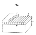
- Figure 1 is a partially cut-away perspective view of an ultrasonic probe.
- the ultrasonic probe is an array-type ultrasonic probe.
- a plurality of piezoelectric elements 1 each having a rectangular shape is fixedly mounted on a backing member 2, and the surfaces of the piezo-electric elements 1 from which surfaces ultrasonic waves are emitted are covered by an acoustic matching layer 3.
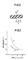
- One of the piezo-electric elements 1 is shown in Figure 2.
- Figure 2 is a cross-sectional view of the piezo-electric element 1, taken along the line A-A' of Figure 1.
- a first electrode 1b and a second electrode 1c are provided respectively on both surfaces of the piezo-electric material 1a in such a way that they are partially overlapped near the center of the piezo-electric material 1a to form a portion D where end portions of the electrodes are facing each other.
- the portions D of the elements 1 are each arranged in a straight fashion throughout the arrayed piezo-electric elements.
- a facing portion D may be achieved, for example, by forming electrodes over the entire surfaces of the piezo-electric material, polling the piezo-electric material 1a in its entirety and then forming the first electrode 1b and the second electrode 1c of desired shapes in accordance with a suitable technique such as the etching technique; or by forming the first electrode 1 b and the second electrode 1c of desired shapes prior to the polling of the piezo-electric material and then subjecting the piezo- electric material to a polling treatment.
- the piezo-electric material 1a is partially polled and an internal strain is hence developed in the piezo-electric material 1a. Therefore, the former process is preferred for actual application.
- a resolution of about 1 mm to 2 mm namely, a beam spread ⁇ + 13° or so is required for such purposes as discovering an affected part in a body at an early stage.
- the frequency is 3.5 MHz and water is used as a transmission medium, it is necessary to reduce the aperture width to 2 mm or so.
- the region of overlap d of the facing portion D below about 2 mm or so by employing such a structure as depicted in Figure 2, thereby providing with ease a piezo-electric element which meets the aforementioned requirements. Since the oscillating surface has a width somewhat broader than the facing portion D where the end portions of the electrodes are facing each other, it is preferable to form the region of overlap d into about one half of the required width, for example, 1 mm or narrower.
- Figure 3 illustrates the relationship between aperture width and beam spread.
- the curve a corresponds to theoretical data of the beam spread A when the region of overlap d of the facing portion D is hypothetically considered to be equal to the aperture width.
- the curve b indicates experimental data of the beam spread 0 for various regions of overlap d of the facing portion D.
- the experimental data have smaller beam spreads 0 than the theoretical data. As described above, it is thus preferred to make the region of overlap d of the required facing portion D smaller than its theoretical value.
- the aperture width of a piezo-electric element can be readily made narrower by incorporating such a structure as described above, it is possible to obtain an ultrasonic probe which can emit ultrasonic beams having a large beam spread. Moreover, since the facing portion D has been formed near the centre of the piezo-electric element, ultrasonic beams having a uniform spread can be emitted.
- FIG. 4 schematically illustrates the detection of a pointA located in an object o with a distance Z apart from the surface of the object o.
- the information of the point A is obtained at various points along the scanning distance d' in the drawing.
- the thus- collected pieces of information are synthetically processed to achieve a resolution of a level similar to the length of the region of overlap d.
- the beam spread ⁇ of a piezo-electric element having an aperture width d is approximated with ⁇ / d in which ⁇ means the wavelength of an ultrasonic wave.
- the beam spread 0 by the synthesized aperture width d' is approximated with ⁇ /d'.
- the above ultrasonic probe may be applied to process signals by the synthetic aperture method in the A-A' direction of Figure 1 and the direction of alignment of a plurality of piezo-electric elements may be set by the focused beam method.
- the spread 0 kept at the level of about 10° or a little wider is very effective.
- Figures 5(a) and 5(c) are cross-sectional views of piezo-electric elements whereas Figure 5(b) is a plan view of a piezo-electric element 1.
- Figures 5(a) and 5(c) are cross-sectional views of piezo-electric elements whereas Figure 5(b) is a plan view of a piezo-electric element 1.
- the manner of formation of the facing portion D by the first and second electrodes 1 b, 1c of the piezo-electric material 1a a is changed.
- Other parts are the same as those depicted in Figure 1.
- outward ends of the electrodes 1 b, 1c are both extended to their corresponding side walls of the piezo-electric material so as to facilitate the leading-out of the electrodes.
- the facing portion D is formed by allowing the electrodes 1 b, 1 c to cross each other. By taking such a structure, the control in region of overlap of the facing portion D is rendered easier.
- the facing portion D is determined by the extent of overlapping of the electrodes 1 b, 1 c. It is however determined by the widths of the electrodes 1 b, 1c irrelevant to the way of their overlapping in the case of Figure 5(b).
- Figure 5(c) illustrates another embodiment of piezo-electric element in which the first electrodes Ibis applied on the entire area of one of the surfaces of the piezoelectric material labutthe second electrode 1c is provided on a part of the other surface.
- the region of overlap of the facing portion D is determined by the width of the second electrode 1c only, thereby facilitating the control of the region of overlap of the facing portion D.
- the piezo-electric elements were fabricated into array-type ultrasonic transducers. It is however possible to bring about substantially the same effects as an array-type ultrasonic transducer by causing a single-type ultrasonic probe, which is formed of a single piece of piezo-electric element, to scan mechanically.
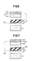
- Figure 6 is a cross-sectional view of a piezoelectric element and acoustic matching layer.
- the piezo-electric element 1 in the present embodiment has the same basic structure as the piezo- electric element depicted in Figure 2.
- the acoustic matching layer has been formed by successively laminating an insulating layer 3a, a conductive layer 3b and a protective layer 3c in order. These layers are arranged in such a way that the protective layer 3c constitutes the outermost layer.
- the conductive layer 3b can be provided, for example, by coating a conductive paste, depositing a metal or adhering a metal foil. It is preferred to make the thickness of the conductive layer 3b sufficiently thin relative to the wavelength so that the conductive layer 3b does not impair the emission and reception of ultrasonic waves by the piezo-electric element.
- the suitable thickness is of the level of 10 ⁇ m or so.
- the protective layer 3c is provided to protect the conductive layer 3b.
- a polymer film having excellent resistance to water and oil and electrically-superb insulating property such as insulating varnish, polyimide, polyester or the like is used. It is also preferred to make the protective layer 3c sufficiently thin, preferably about 10 ⁇ m in thickness, relative to the wavelength so that the protective layer 3c does not impair the emission and reception of ultrasonic waves by the piezo-electric element. Where it is unnecessary to provide the conductive layer 3b with resistance to water, oil, etc., it is not required to provide the protective layer 3c additionally. It is however preferred to provide, generally speaking, the protective layer 3c because an ultrasonic probe is normally used to emit ultrasonic wave into an object through water, oil or the like.
- Such conductive layer 3b and protective layer 3c may be provided at once if a printed flexible sheet having a conductive layer such as copper foil and made of a polyester, polyimide or the like is used. This is very advantageous from the viewpoint of fabrication. Where the insulating layer 3a is formed of a plurality of layers, it is unnecessary to provide any additional protective film if the conductive layer 3b is provided between such insulating layers.
- the acoustic matching layer 3 is formed generally with a thickness equivalent to one fourth of the wavelength ⁇ of ultrasonic waves.
- the acoustic matching layer has heretofore been formed of an insulating layer only.
- the insulating layer has conventionally had a thickness of ⁇ /4.
- an ultrasonic probe of the aforementioned structure was fabricated.
- the ultrasonic probe was then driven in accordance with the synthetic aperture method.
- a resolution of the level of 1 to 1.5 mm or so was achieved irrespective of the depth of an interested point in an object.
- the ultrasonic probe was free from the intrusion of noises from the outside and gave a dynamic range of 80 dB or higher and a good S/N ratio.
- Figure 7 has the same structure as the embodiment depicted in Figure 6 except that the combination of grounding of the electrodes 1b, 1c and the conductive layer 3b has been changed.
- Figure 7 is a cross-sectional view similar to Figure 6.
- the conductive layer 3b and the electrode 1c which is located at the side of the backing member 2 are grounded whereas a voltage is applied to the electrode 1 b.
- the conductive layer 3b which is provided to form an electromagnetic shield was also grounded as shown in Figure 6. In this case, the potential between the conductive layer 3b and electrode 1c may be applied to a non-electrode portion of the ultrasonic wave emitting surface of the piezo- electric element 1 which portion is not covered by the electrode 1c and spurious oscillations may thus be developed.
- Provision of the conductive layer 3b as in the present invention can prevent electrical effects to the outside, whereby making it unnecessary to additionally ground the electrode 1c placed on the ultrasonic wave emitting surface of the piezoelectric element 1. As illustrated in Figure 7, the electrode 1c is thus grounded when driving the ultrasonic probe. Where such a structure as mentioned above is employed, no potential difference is allowed to occur between the electrode 1c and conductive layer 3b and there is thus no danger to produce such spurious oscillations as mentioned above.
- the embodiment of this invention which is shown in Figure 8, is fabricated by using a material, in which ultrasonic waves are attenuated considerably, to form an insulating member 3a' for a part which is in contact with a non-electrode portion of the ultrasonic wave emitting surface of the piezo-electric element 1 which portion is not covered by the electrode 1 b.
- the remaining parts of the structure is similar to those of the embodiment shown in Figure 6.
- Figure 8 is a cross-sectional view similar to Figure 6.
- the conductive layer 3b is not always necessary to have the conductive layer 3b cover the entire area of the surface of the piezo-electric element 1.
- the conductive layer 3b is provided on a part of the corresponding surface of the piezo-electric element 1 with the insulating layer 3a interposed therebetween. The remaining parts of the structure are the same as those of the embodiment illustrated in Figure 6.
- Figure 9 is a cross-sectional view similar to Figure 6.
- the conductive layer 3b is applied in such a way that it covers only a part of the ultrasonic wave emitting surface of the piezo-electric element 1 which part is not covered by the electrode 1 b.
- the electrode 1b serves as a shield for the surface of the piezoelectric element 1.
Claims (11)
caractérisée en ce que:
Applications Claiming Priority (2)
| Application Number | Priority Date | Filing Date | Title |
|---|---|---|---|
| JP207701/82 | 1982-11-29 | ||
| JP57207701A JPS5999900A (ja) | 1982-11-29 | 1982-11-29 | 超音波探触子 |
Publications (4)
| Publication Number | Publication Date |
|---|---|
| EP0110378A2 EP0110378A2 (fr) | 1984-06-13 |
| EP0110378A3 EP0110378A3 (en) | 1985-05-15 |
| EP0110378B1 EP0110378B1 (fr) | 1989-03-01 |
| EP0110378B2 true EP0110378B2 (fr) | 1994-06-22 |
Family
ID=16544132
Family Applications (1)
| Application Number | Title | Priority Date | Filing Date |
|---|---|---|---|
| EP83111954A Expired - Lifetime EP0110378B2 (fr) | 1982-11-29 | 1983-11-29 | Sonde ultrasonore |
Country Status (5)
| Country | Link |
|---|---|
| US (1) | US4583018A (fr) |
| EP (1) | EP0110378B2 (fr) |
| JP (1) | JPS5999900A (fr) |
| AU (1) | AU553274B2 (fr) |
| DE (1) | DE3379286D1 (fr) |
Families Citing this family (17)
| Publication number | Priority date | Publication date | Assignee | Title |
|---|---|---|---|---|
| IN161925B (fr) * | 1984-11-29 | 1988-02-27 | Siemens Ag | |
| JPH0832107B2 (ja) * | 1986-01-31 | 1996-03-27 | 富士通株式会社 | 圧電振動子 |
| JPH063437B2 (ja) * | 1987-03-31 | 1994-01-12 | 鈴幸精密工業株式会社 | 超音波探触子 |
| DE3720574A1 (de) * | 1987-06-22 | 1989-01-05 | Deutsch Pruef Messgeraete | Ultraschall-mehrfachpruefkopf |
| JP2615132B2 (ja) * | 1988-05-19 | 1997-05-28 | 富士通株式会社 | 超音波探触子 |
| US5446333A (en) * | 1992-09-21 | 1995-08-29 | Ngk Insulators, Ltd. | Ultrasonic transducers |
| US20030173870A1 (en) * | 2002-03-12 | 2003-09-18 | Shuh-Yueh Simon Hsu | Piezoelectric ultrasound transducer assembly having internal electrodes for bandwidth enhancement and mode suppression |
| DE10335331A1 (de) * | 2003-08-01 | 2005-03-03 | Epcos Ag | Elektrisches Bauelement mit überlappenden Elektroden und Verfahren zur Herstellung |
| EP1937150A4 (fr) * | 2005-09-27 | 2010-01-20 | Medison Co Ltd | Sonde de diagnostic ultrasons et système de diagnostic ultrasons l'utilisant |
| US8058776B1 (en) * | 2006-11-27 | 2011-11-15 | William Gordon Gibson | Laminar array ultrasound transducer and system |
| JP5038865B2 (ja) * | 2007-11-22 | 2012-10-03 | 株式会社東芝 | 超音波探触子、超音波診断装置、及び超音波探触子の製造方法 |
| WO2012086180A1 (fr) * | 2010-12-20 | 2012-06-28 | Necカシオモバイルコミュニケーションズ株式会社 | Dispositif d'oscillateur et instrument électronique |
| JP5738671B2 (ja) * | 2011-05-18 | 2015-06-24 | 株式会社東芝 | 超音波トランスデューサ、超音波プローブおよび超音波トランスデューサの製造方法 |
| JP5823322B2 (ja) * | 2012-03-14 | 2015-11-25 | 富士フイルム株式会社 | 光音響装置、光音響装置用プローブおよび音響波検出信号の取得方法 |
| ES2809878T3 (es) * | 2012-10-02 | 2021-03-08 | Flodesign Sonics Inc | Tecnología de separación acustoforética que utiliza ondas estacionarias multidimensionales |
| JP6724502B2 (ja) * | 2016-04-06 | 2020-07-15 | セイコーエプソン株式会社 | 超音波装置 |
| US10518293B2 (en) * | 2016-12-09 | 2019-12-31 | Sensus USA, Inc. | Thickness-planar mode transducers and related devices |
Family Cites Families (11)
| Publication number | Priority date | Publication date | Assignee | Title |
|---|---|---|---|---|
| GB1208154A (en) * | 1968-02-13 | 1970-10-07 | Mullard Ltd | Improvements in or relating to acoustical transducers |
| JPS5512254B2 (fr) * | 1973-07-03 | 1980-03-31 | ||
| JPS5824080B2 (ja) * | 1978-09-20 | 1983-05-19 | 株式会社東芝 | 超音波送受波器 |
| US4211948A (en) * | 1978-11-08 | 1980-07-08 | General Electric Company | Front surface matched piezoelectric ultrasonic transducer array with wide field of view |
| AT364438B (de) * | 1979-03-12 | 1981-10-27 | Kretztechnik Gmbh | Schallkopf fuer untersuchungen mit ultraschall nach dem impuls-echoverfahren |
| US4217684A (en) * | 1979-04-16 | 1980-08-19 | General Electric Company | Fabrication of front surface matched ultrasonic transducer array |
| US4482834A (en) * | 1979-06-28 | 1984-11-13 | Hewlett-Packard Company | Acoustic imaging transducer |
| US4395652A (en) * | 1979-09-13 | 1983-07-26 | Toray Industries, Inc. | Ultrasonic transducer element |
| US4277712A (en) * | 1979-10-11 | 1981-07-07 | Hewlett-Packard Company | Acoustic electric transducer with slotted base |
| JPS593080B2 (ja) | 1980-03-06 | 1984-01-21 | 横河電機株式会社 | 超音波探触子 |
| FR2531298B1 (fr) * | 1982-07-30 | 1986-06-27 | Thomson Csf | Transducteur du type demi-onde a element actif en polymere piezoelectrique |
-
1982
- 1982-11-29 JP JP57207701A patent/JPS5999900A/ja active Pending
-
1983
- 1983-11-24 AU AU21652/83A patent/AU553274B2/en not_active Ceased
- 1983-11-25 US US06/555,049 patent/US4583018A/en not_active Expired - Lifetime
- 1983-11-29 EP EP83111954A patent/EP0110378B2/fr not_active Expired - Lifetime
- 1983-11-29 DE DE8383111954T patent/DE3379286D1/de not_active Expired
Also Published As
| Publication number | Publication date |
|---|---|
| AU2165283A (en) | 1984-06-07 |
| AU553274B2 (en) | 1986-07-10 |
| JPS5999900A (ja) | 1984-06-08 |
| EP0110378A3 (en) | 1985-05-15 |
| EP0110378A2 (fr) | 1984-06-13 |
| EP0110378B1 (fr) | 1989-03-01 |
| US4583018A (en) | 1986-04-15 |
| DE3379286D1 (en) | 1989-04-06 |
Similar Documents
| Publication | Publication Date | Title |
|---|---|---|
| EP0110378B2 (fr) | Sonde ultrasonore | |
| US4460841A (en) | Ultrasonic transducer shading | |
| US4825115A (en) | Ultrasonic transducer and method for fabricating thereof | |
| EP0342874B1 (fr) | Transducteur à ultrasons pour un dispositif d'imagerie médical | |
| US5115810A (en) | Ultrasonic transducer array | |
| EP0210723B1 (fr) | Transducteur ultrason | |
| KR100695504B1 (ko) | 초음파 직선 또는 곡선 변환기 및 그 접속 방법 | |
| US4371805A (en) | Ultrasonic transducer arrangement and method for fabricating same | |
| US6308389B1 (en) | Ultrasonic transducer and manufacturing method therefor | |
| US5706820A (en) | Ultrasonic transducer with reduced elevation sidelobes and method for the manufacture thereof | |
| EP0785826B1 (fr) | Matrice de transducteurs a ultrasons soumis a une apodisation de la focalisation en elevation | |
| EP0637469A2 (fr) | Elément transducteur à couches multiples | |
| JPS597280B2 (ja) | インピ−ダンス整合装置及びそれを用いた音響変換器組立体 | |
| EP0212737B1 (fr) | Dispositif d'imagerie ultrasonore | |
| US8269400B2 (en) | Ultrasonic transducer, ultrasonic diagnosis apparatus using the same, and ultrasonic flaw inspection apparatus using the same | |
| US5657295A (en) | Ultrasonic transducer with adjustable elevational aperture and methods for using same | |
| JP3883822B2 (ja) | 配列型の超音波探触子 | |
| EP1700641A1 (fr) | Sonde endocavitaire à ultrasons | |
| DE3149732A1 (de) | Ultraschallwandleranordnung | |
| JPH0120615B2 (fr) | ||
| JPH0349389B2 (fr) | ||
| KR102623559B1 (ko) | 초음파 프로브 | |
| JP3731690B2 (ja) | 超音波探触子 | |
| JPS63276400A (ja) | 超音波探触子とその製造方法 | |
| JPH0538335A (ja) | 超音波探触子およびその製造方法 |
Legal Events
| Date | Code | Title | Description |
|---|---|---|---|
| PUAI | Public reference made under article 153(3) epc to a published international application that has entered the european phase |
Free format text: ORIGINAL CODE: 0009012 |
|
| AK | Designated contracting states |
Designated state(s): DE FR GB NL |
|
| RAP1 | Party data changed (applicant data changed or rights of an application transferred) |
Owner name: KABUSHIKI KAISHA TOSHIBA |
|
| PUAL | Search report despatched |
Free format text: ORIGINAL CODE: 0009013 |
|
| AK | Designated contracting states |
Designated state(s): DE FR GB NL |
|
| 17P | Request for examination filed |
Effective date: 19851014 |
|
| 17Q | First examination report despatched |
Effective date: 19870206 |
|
| GRAA | (expected) grant |
Free format text: ORIGINAL CODE: 0009210 |
|
| AK | Designated contracting states |
Kind code of ref document: B1 Designated state(s): DE FR GB NL |
|
| REF | Corresponds to: |
Ref document number: 3379286 Country of ref document: DE Date of ref document: 19890406 |
|
| ET | Fr: translation filed | ||
| PG25 | Lapsed in a contracting state [announced via postgrant information from national office to epo] |
Ref country code: GB Effective date: 19891129 |
|
| PLBI | Opposition filed |
Free format text: ORIGINAL CODE: 0009260 |
|
| 26 | Opposition filed |
Opponent name: SIEMENS AKTIENGESELLSCHAFT, BERLIN UND MUENCHEN Effective date: 19891130 |
|
| NLR1 | Nl: opposition has been filed with the epo |
Opponent name: SIEMENS AG. |
|
| GBPC | Gb: european patent ceased through non-payment of renewal fee | ||
| PUAH | Patent maintained in amended form |
Free format text: ORIGINAL CODE: 0009272 |
|
| STAA | Information on the status of an ep patent application or granted ep patent |
Free format text: STATUS: PATENT MAINTAINED AS AMENDED |
|
| 27A | Patent maintained in amended form |
Effective date: 19940622 |
|
| AK | Designated contracting states |
Kind code of ref document: B2 Designated state(s): DE FR GB NL |
|
| ET3 | Fr: translation filed ** decision concerning opposition | ||
| NLR2 | Nl: decision of opposition | ||
| NLR3 | Nl: receipt of modified translations in the netherlands language after an opposition procedure | ||
| PGFP | Annual fee paid to national office [announced via postgrant information from national office to epo] |
Ref country code: FR Payment date: 19961111 Year of fee payment: 14 |
|
| PGFP | Annual fee paid to national office [announced via postgrant information from national office to epo] |
Ref country code: NL Payment date: 19961128 Year of fee payment: 14 |
|
| PGFP | Annual fee paid to national office [announced via postgrant information from national office to epo] |
Ref country code: DE Payment date: 19961206 Year of fee payment: 14 |
|
| PG25 | Lapsed in a contracting state [announced via postgrant information from national office to epo] |
Ref country code: FR Free format text: THE PATENT HAS BEEN ANNULLED BY A DECISION OF A NATIONAL AUTHORITY Effective date: 19971130 |
|
| PG25 | Lapsed in a contracting state [announced via postgrant information from national office to epo] |
Ref country code: NL Free format text: LAPSE BECAUSE OF NON-PAYMENT OF DUE FEES Effective date: 19980601 |
|
| PG25 | Lapsed in a contracting state [announced via postgrant information from national office to epo] |
Ref country code: DE Free format text: LAPSE BECAUSE OF NON-PAYMENT OF DUE FEES Effective date: 19980801 |
|
| NLV4 | Nl: lapsed or anulled due to non-payment of the annual fee |
Effective date: 19980601 |
|
| REG | Reference to a national code |
Ref country code: FR Ref legal event code: ST |