EP0103468A2 - Analog-Digital-Wandlersystem - Google Patents
Analog-Digital-Wandlersystem Download PDFInfo
- Publication number
- EP0103468A2 EP0103468A2 EP83305274A EP83305274A EP0103468A2 EP 0103468 A2 EP0103468 A2 EP 0103468A2 EP 83305274 A EP83305274 A EP 83305274A EP 83305274 A EP83305274 A EP 83305274A EP 0103468 A2 EP0103468 A2 EP 0103468A2
- Authority
- EP
- European Patent Office
- Prior art keywords
- digital
- analog
- span
- converter
- conversion system
- Prior art date
- Legal status (The legal status is an assumption and is not a legal conclusion. Google has not performed a legal analysis and makes no representation as to the accuracy of the status listed.)
- Withdrawn
Links
- 238000006243 chemical reaction Methods 0.000 title claims description 13
- 230000008878 coupling Effects 0.000 claims 1
- 238000010168 coupling process Methods 0.000 claims 1
- 238000005859 coupling reaction Methods 0.000 claims 1
- 238000000034 method Methods 0.000 claims 1
- 229920005994 diacetyl cellulose Polymers 0.000 description 2
- 238000004364 calculation method Methods 0.000 description 1
- 238000010586 diagram Methods 0.000 description 1
- 230000003292 diminished effect Effects 0.000 description 1
- 238000006073 displacement reaction Methods 0.000 description 1
- 239000004065 semiconductor Substances 0.000 description 1
Images
Classifications
-
- H—ELECTRICITY
- H03—ELECTRONIC CIRCUITRY
- H03M—CODING; DECODING; CODE CONVERSION IN GENERAL
- H03M1/00—Analogue/digital conversion; Digital/analogue conversion
- H03M1/10—Calibration or testing
-
- H—ELECTRICITY
- H03—ELECTRONIC CIRCUITRY
- H03M—CODING; DECODING; CODE CONVERSION IN GENERAL
- H03M1/00—Analogue/digital conversion; Digital/analogue conversion
- H03M1/12—Analogue/digital converters
- H03M1/1205—Multiplexed conversion systems
Definitions
- the present invention relates to an analog-to-digital signal conversion system.
- ADC analog-to-digital converter
- An object of the present invention is to provide efficient analog-to-digital conversion of a plurality of sensed values.
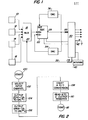
- a control system may include a plurality of parameter sensors 10, 12, 14 and 16 for measuring such physical parameters such as pressure, temperature, force, displacement, etc.
- the analog output signals of sensors 10-16 may vary in voltage span or range and offset.
- sensor 10 may have an output voltage range of 2.0 to 4.0 volts; sensor 12 a range of 3.5 to 4.5 volts; sensor 14 a range of 0.5 to 1.5 volts and sensor 16 a range of 0 to 5.0 volts.
- the outputs of the sensors 10-16 are coupled to respective inputs of a conventional analog multiplexer 18 which includes address control inputs 20.
- the output of the multiplexer 18 is coupled to the analog input of an analog-to-digital converter (ADC) 22.
- ADC analog-to-digital converter
- the ADC is a conventional successive approximation-type, such as National Semiconductor Part No ADC-0801, which includes a resistor ladder (not shown).
- the ADC outputs 28 communicate a digital 8-bit parallel output signals to a data processing unit 30, such as a microprocessor.
- the data processing unit 30 operates upon the data received from-the ADC 22, according to any desired control algorithm which forms no part of the present invention.
- the data processing unit 30 generates address control signals which are applied to the multiplexer 18 via lines 32.
- the data processor 30 also generates digital calibration control signals which are applied to conventional digital-to-analog converters (DAC) 34 and 36.
- DACs 34 and 36 convert the digital calibration signals to analog offset and span calibration signals which are applied to the IN- and RED terminals respectively of the ADC 22.
- the microprocessor 30 is also coupled with a non-volatile memory (NOVRAM) 40 and a grounded switch 42 which are used in connection with a calibration scheme which will be described next.
- NOVRAM non-volatile memory
- An automatic calibration scheme may be implemented in the following manner. First, switch 42 is opened to inform the microprocessor 30 that the operator is performing a calibration. DAC 34 is then set to apply 0 volts to the IN- input of ADC 22 and DAC 36 is set to apply its maximum output, 5 volts, for example, to the REF input of ADC 22. Each sensor (10-16) is then exercised over its full operating range and the microprocessor 30 is made to store the minimum and maximum values for each sensor. The switch 42 is then closed after which the sensor minimum values are stored in the non-volatile memory 40 for use as the offset value which is applied to the IN- input of ADC 22 via DAC 34 every time the corresponding sensor is read.
- the microprocessor 3 0 then subtracts the minimum value, from the maximum value for each sensor and stores the resultant difference value in the non-volatile memory 40 as a "span" value. Then, each time a particular sensor output is digitized, the corresponding span value is applied to the REF input of ADC 22 via DAC 36.
- a conversion routine is executed whenever a value from one of the sensors 10-16 is to be read into the data. processing unit 30 via ADC 22. This conversion routine will now be described with reference to the flow chart shown in Fig 2.
- the conversion routine begins at step 100. Then, at step 102, the data processing unit 30 sends an address signal to the multiplexer 18 so that the analog voltage from the selected sensor will be applied to the IN+ input of A DC 22. Then, in step 104, the offset digital calibration value (stored in memory) is applied to DAC 34. Then, in step 106, the span digital calibration value (stored in memory) is applied to DAC 36.
- analog voltage equivalents of the stored offset and span values will be applied to the IN- and REF inputs of ADC 22 via DACs 34 and 36.
- the analog value applied to the IN+ input of ADC 22 is converted with-full 8-bit resolution to a corresponding digital value which is contained in an output register (not shown) in the ADC 22.
- the conversion is in each case normalized in accordance with the offset value and the span value so that the digital range for every parameter is the same, e.g. 0 to 11111111 in the case of an unsigned 8-bit system.
- This digital value is then read by the data processor unit 30.
- This conversion routine is completed at step 112 and is repeated for each of sensors 10-16 with different offset and span calibration values chosen for each different sensor. In this manner, the digital value will be obtained with the full resolution capability of the ADC 22, regardless of the different span and offsets of the analog output voltages provided by the different sensors.
Landscapes
- Engineering & Computer Science (AREA)
- Theoretical Computer Science (AREA)
- Analogue/Digital Conversion (AREA)
Applications Claiming Priority (2)
| Application Number | Priority Date | Filing Date | Title |
|---|---|---|---|
| US41723882A | 1982-09-13 | 1982-09-13 | |
| US417238 | 1995-04-05 |
Publications (1)
| Publication Number | Publication Date |
|---|---|
| EP0103468A2 true EP0103468A2 (de) | 1984-03-21 |
Family
ID=23653149
Family Applications (1)
| Application Number | Title | Priority Date | Filing Date |
|---|---|---|---|
| EP83305274A Withdrawn EP0103468A2 (de) | 1982-09-13 | 1983-09-09 | Analog-Digital-Wandlersystem |
Country Status (3)
| Country | Link |
|---|---|
| EP (1) | EP0103468A2 (de) |
| JP (1) | JPS5972223A (de) |
| AU (1) | AU1802583A (de) |
Cited By (2)
| Publication number | Priority date | Publication date | Assignee | Title |
|---|---|---|---|---|
| EP0495280A1 (de) * | 1991-01-18 | 1992-07-22 | International Business Machines Corporation | Analog-Digitalwandler mit Driftkompensation |
| WO1999017452A1 (en) * | 1997-09-30 | 1999-04-08 | Trustees Of Princeton University | High-speed serial-to-parallel and analog-to-digital conversion |
Families Citing this family (1)
| Publication number | Priority date | Publication date | Assignee | Title |
|---|---|---|---|---|
| JPS61117924A (ja) * | 1984-11-13 | 1986-06-05 | Sony Corp | 画像補正装置 |
-
1983
- 1983-08-16 AU AU18025/83A patent/AU1802583A/en not_active Abandoned
- 1983-09-09 EP EP83305274A patent/EP0103468A2/de not_active Withdrawn
- 1983-09-13 JP JP58169112A patent/JPS5972223A/ja active Pending
Cited By (5)
| Publication number | Priority date | Publication date | Assignee | Title |
|---|---|---|---|---|
| US5179379A (en) * | 1990-01-18 | 1993-01-12 | International Business Machines Corporation | Analog to digital convertor with drift compensation |
| EP0495280A1 (de) * | 1991-01-18 | 1992-07-22 | International Business Machines Corporation | Analog-Digitalwandler mit Driftkompensation |
| WO1999017452A1 (en) * | 1997-09-30 | 1999-04-08 | Trustees Of Princeton University | High-speed serial-to-parallel and analog-to-digital conversion |
| US6265999B1 (en) | 1997-09-30 | 2001-07-24 | Trustees Of Princeton University | High-speed serial-to-parallel and analog-to-digital conversion |
| US6433715B2 (en) | 1997-09-30 | 2002-08-13 | Trustees Of Princeton University | High-speed serial-to-parallel and analog-to-digital conversion |
Also Published As
| Publication number | Publication date |
|---|---|
| JPS5972223A (ja) | 1984-04-24 |
| AU1802583A (en) | 1984-03-22 |
Similar Documents
| Publication | Publication Date | Title |
|---|---|---|
| US5361067A (en) | Digital linearization calibration for analog to digital converter | |
| US6191715B1 (en) | System for calibration of a digital-to-analog converter | |
| US4612533A (en) | Harmonic distortion reduction technique for data acquistion | |
| US5172115A (en) | Ratiometric A/D converter with non-rationometric error offset | |
| EP0709971A2 (de) | Sigma Delta Analog-Digital Wandler mit 3 Punkt Kalibriervorrichtung und Kalibrierverfahren | |
| US7755521B1 (en) | A-D convert apparatus, D-A convert apparatus and adjustment method | |
| EP0698315A1 (de) | Algorithmischer analog-/digitalwandler mit digitalem kalibriertem ausgang | |
| JPS58181323A (ja) | 較正機能付きデジタルアナログ変換器 | |
| US20090212987A1 (en) | Variable quantization adc for image sensors | |
| US4903024A (en) | A/D converter system with error correction and calibration apparatus and method | |
| GB2138228A (en) | Method and circuit for measuring nonlinearity in dual flash analog to digital converter | |
| US6720896B2 (en) | Analog/digital or digital/analog converter having internal reference voltage selection | |
| US4857931A (en) | Dual flash analog-to-digital converter | |
| US5041832A (en) | Dual flash analog-to-digital converter | |
| JPS5873231A (ja) | Ad変換装置 | |
| EP1510007B1 (de) | Offsetkalibrationssystem | |
| EP0103468A2 (de) | Analog-Digital-Wandlersystem | |
| JPH07326970A (ja) | A/d変換器及びa/d変換器のテスト方法 | |
| US5206649A (en) | Dual flash analog-to-digital converter | |
| JPS5912619A (ja) | アナログ・デイジタル変換器の自動補正方法 | |
| US5099241A (en) | Dual flash analog-to-digital converter | |
| JPH06334523A (ja) | アナログ−ディジタル変換装置 | |
| JPH06204870A (ja) | 自動補正機能付d/a変換器 | |
| JPS58186841A (ja) | 対数変換装置 | |
| JPS5928294B2 (ja) | Ad変換器 |
Legal Events
| Date | Code | Title | Description |
|---|---|---|---|
| PUAI | Public reference made under article 153(3) epc to a published international application that has entered the european phase |
Free format text: ORIGINAL CODE: 0009012 |
|
| AK | Designated contracting states |
Designated state(s): AT BE CH DE FR GB IT LI NL SE |
|
| STAA | Information on the status of an ep patent application or granted ep patent |
Free format text: STATUS: THE APPLICATION HAS BEEN WITHDRAWN |
|
| 18W | Application withdrawn |
Withdrawal date: 19840320 |
|
| RIN1 | Information on inventor provided before grant (corrected) |
Inventor name: NICHOLS, BOYD MORTON |