EP0103352B1 - Magnetischer Sensor, insbesondere Wiedergabekopf für magnetisches Aufzeichnungsmedium - Google Patents
Magnetischer Sensor, insbesondere Wiedergabekopf für magnetisches Aufzeichnungsmedium Download PDFInfo
- Publication number
- EP0103352B1 EP0103352B1 EP83303179A EP83303179A EP0103352B1 EP 0103352 B1 EP0103352 B1 EP 0103352B1 EP 83303179 A EP83303179 A EP 83303179A EP 83303179 A EP83303179 A EP 83303179A EP 0103352 B1 EP0103352 B1 EP 0103352B1
- Authority
- EP
- European Patent Office
- Prior art keywords
- stratum
- magnetostrictive
- piezoresistive
- thin film
- magnetic
- Prior art date
- Legal status (The legal status is an assumption and is not a legal conclusion. Google has not performed a legal analysis and makes no representation as to the accuracy of the status listed.)
- Expired
Links
- 239000010409 thin film Substances 0.000 claims abstract description 50
- 239000000463 material Substances 0.000 claims abstract description 22
- 239000007787 solid Substances 0.000 claims abstract description 5
- 239000000758 substrate Substances 0.000 claims description 39
- 230000008859 change Effects 0.000 claims description 10
- 230000035699 permeability Effects 0.000 claims description 10
- 230000004907 flux Effects 0.000 claims description 9
- 239000004065 semiconductor Substances 0.000 claims description 5
- 230000008878 coupling Effects 0.000 claims description 4
- 238000010168 coupling process Methods 0.000 claims description 4
- 238000005859 coupling reaction Methods 0.000 claims description 4
- 230000004044 response Effects 0.000 claims description 3
- 239000013078 crystal Substances 0.000 claims 1
- 239000010408 film Substances 0.000 abstract description 47
- XUIMIQQOPSSXEZ-UHFFFAOYSA-N Silicon Chemical compound [Si] XUIMIQQOPSSXEZ-UHFFFAOYSA-N 0.000 description 9
- 229910052710 silicon Inorganic materials 0.000 description 9
- 239000010703 silicon Substances 0.000 description 9
- 230000001939 inductive effect Effects 0.000 description 7
- 108091006146 Channels Proteins 0.000 description 5
- 238000005513 bias potential Methods 0.000 description 4
- 238000010276 construction Methods 0.000 description 4
- 238000000034 method Methods 0.000 description 4
- 238000004804 winding Methods 0.000 description 4
- PXHVJJICTQNCMI-UHFFFAOYSA-N Nickel Chemical compound [Ni] PXHVJJICTQNCMI-UHFFFAOYSA-N 0.000 description 3
- 238000000151 deposition Methods 0.000 description 3
- 230000015654 memory Effects 0.000 description 3
- 239000000853 adhesive Substances 0.000 description 2
- 230000001070 adhesive effect Effects 0.000 description 2
- 229910052782 aluminium Inorganic materials 0.000 description 2
- XAGFODPZIPBFFR-UHFFFAOYSA-N aluminium Chemical compound [Al] XAGFODPZIPBFFR-UHFFFAOYSA-N 0.000 description 2
- 239000004020 conductor Substances 0.000 description 2
- 230000003247 decreasing effect Effects 0.000 description 2
- 238000005516 engineering process Methods 0.000 description 2
- 238000004519 manufacturing process Methods 0.000 description 2
- 239000000203 mixture Substances 0.000 description 2
- 239000004593 Epoxy Substances 0.000 description 1
- 229910002555 FeNi Inorganic materials 0.000 description 1
- 229910005347 FeSi Inorganic materials 0.000 description 1
- 108090000699 N-Type Calcium Channels Proteins 0.000 description 1
- 108010075750 P-Type Calcium Channels Proteins 0.000 description 1
- 229910000676 Si alloy Inorganic materials 0.000 description 1
- 229910045601 alloy Inorganic materials 0.000 description 1
- 239000000956 alloy Substances 0.000 description 1
- 230000003321 amplification Effects 0.000 description 1
- 239000000969 carrier Substances 0.000 description 1
- 239000000919 ceramic Substances 0.000 description 1
- 230000008021 deposition Effects 0.000 description 1
- 238000001514 detection method Methods 0.000 description 1
- 230000009977 dual effect Effects 0.000 description 1
- 230000000694 effects Effects 0.000 description 1
- 239000011521 glass Substances 0.000 description 1
- 239000012212 insulator Substances 0.000 description 1
- 238000010884 ion-beam technique Methods 0.000 description 1
- XWHPIFXRKKHEKR-UHFFFAOYSA-N iron silicon Chemical compound [Si].[Fe] XWHPIFXRKKHEKR-UHFFFAOYSA-N 0.000 description 1
- 238000002955 isolation Methods 0.000 description 1
- 230000005415 magnetization Effects 0.000 description 1
- 229910052751 metal Inorganic materials 0.000 description 1
- 239000002184 metal Substances 0.000 description 1
- 229910044991 metal oxide Inorganic materials 0.000 description 1
- 150000004706 metal oxides Chemical class 0.000 description 1
- 238000005065 mining Methods 0.000 description 1
- 238000003199 nucleic acid amplification method Methods 0.000 description 1
- 230000008569 process Effects 0.000 description 1
- 125000006850 spacer group Chemical group 0.000 description 1
- 238000003860 storage Methods 0.000 description 1
Images
Classifications
-
- G—PHYSICS
- G01—MEASURING; TESTING
- G01R—MEASURING ELECTRIC VARIABLES; MEASURING MAGNETIC VARIABLES
- G01R33/00—Arrangements or instruments for measuring magnetic variables
- G01R33/02—Measuring direction or magnitude of magnetic fields or magnetic flux
- G01R33/06—Measuring direction or magnitude of magnetic fields or magnetic flux using galvano-magnetic devices
-
- G—PHYSICS
- G11—INFORMATION STORAGE
- G11B—INFORMATION STORAGE BASED ON RELATIVE MOVEMENT BETWEEN RECORD CARRIER AND TRANSDUCER
- G11B5/00—Recording by magnetisation or demagnetisation of a record carrier; Reproducing by magnetic means; Record carriers therefor
- G11B5/127—Structure or manufacture of heads, e.g. inductive
- G11B5/1278—Structure or manufacture of heads, e.g. inductive specially adapted for magnetisations perpendicular to the surface of the record carrier
-
- G—PHYSICS
- G11—INFORMATION STORAGE
- G11B—INFORMATION STORAGE BASED ON RELATIVE MOVEMENT BETWEEN RECORD CARRIER AND TRANSDUCER
- G11B5/00—Recording by magnetisation or demagnetisation of a record carrier; Reproducing by magnetic means; Record carriers therefor
- G11B5/127—Structure or manufacture of heads, e.g. inductive
- G11B5/33—Structure or manufacture of flux-sensitive heads, i.e. for reproduction only; Combination of such heads with means for recording or erasing only
- G11B5/332—Structure or manufacture of flux-sensitive heads, i.e. for reproduction only; Combination of such heads with means for recording or erasing only using thin films
-
- G—PHYSICS
- G11—INFORMATION STORAGE
- G11B—INFORMATION STORAGE BASED ON RELATIVE MOVEMENT BETWEEN RECORD CARRIER AND TRANSDUCER
- G11B5/00—Recording by magnetisation or demagnetisation of a record carrier; Reproducing by magnetic means; Record carriers therefor
- G11B5/48—Disposition or mounting of heads or head supports relative to record carriers ; arrangements of heads, e.g. for scanning the record carrier to increase the relative speed
- G11B5/58—Disposition or mounting of heads or head supports relative to record carriers ; arrangements of heads, e.g. for scanning the record carrier to increase the relative speed with provision for moving the head for the purpose of maintaining alignment of the head relative to the record carrier during transducing operation, e.g. to compensate for surface irregularities of the latter or for track following
-
- H—ELECTRICITY
- H10—SEMICONDUCTOR DEVICES; ELECTRIC SOLID-STATE DEVICES NOT OTHERWISE PROVIDED FOR
- H10N—ELECTRIC SOLID-STATE DEVICES NOT OTHERWISE PROVIDED FOR
- H10N35/00—Magnetostrictive devices
- H10N35/101—Magnetostrictive devices with mechanical input and electrical output, e.g. generators, sensors
Definitions
- This invention relates to magnetic recording playbacks heads, particularly to such heads wherein non-inductive means are utilized for sensing localized magnetic field patterns of a magnetic recording medium.
- Such thin film heads were perhaps first disclosed in U.S. Patent US-A-3,344,237 assigned to Minnesota Mining and Manufacturing Company, the assignee of the present invention. Since the initial development, many types of thin film heads have been developed in various attempts to improve the reliability and signal-to-noise ratio while reducing manufacturing costs, complexity, and the like. Relevant to the present invention are non-inductive thin film playback heads, such as those utilizing magneto-resistive films.
- U.S. Patent US-A-3,987,485 (Sugaya et al) is exemplary of prior art disclosing such heads.
- the device there disclosed includes a semiconductive substrate on which may be deposited, along with the magnetoresistive film, or films for multitrack heads, integrated circuits such as switching circuits and amplifiers which are connected to the magnetic heads.
- a semiconductive substrate on which may be deposited, along with the magnetoresistive film, or films for multitrack heads, integrated circuits such as switching circuits and amplifiers which are connected to the magnetic heads.
- U.S. Patent US-A-3,908,194 depicts a thin film magnetoresistive read head integrated with a thin film inductive write head.
- magnetoresistive thin film heads it is also known to utilize heads including thin films having magnetostrictive properties.
- heads including thin films having magnetostrictive properties For example, Brunsch et al, IBM Tech. Disclosure Bulletin, Vol. 21, No. 2, July 1978, pp. 667-668, depicts a thin film head, with both read and write capabilities, in which magnetostrictive films having permanent anisotropy surround a single turn inductive winding, forming a working gap therebetween, and are in turn mechanically coupled to a piezoelectric substrate.
- read or write signals appear to be coupled from or to the conductor and hence inductively from or to the gap, while DC or AC voltages are applied to the piezoelectric substrate, causing stress in the magnetostrictive films, which, in turn, rotates the anisotropy to allow the signals to be more readily coupled through the gap.
- Such a head is thus actually an inductive type device in which magnetostriction is utilized in a secondary manner.
- US-A-3 800 193 discloses a magnetic sensing head in which the magnetic flux sensitive device is formed as a film on a semiconductor substrate but there is no suggestion in this reference of the use of a strain sensitive element as required by the present invention.
- IBM Technical Disclosure Bulletin, Vol. 17, No. 11, April 1975, pages 3478-3480 disclose a magnetoresistive head but there is no disclosure of a magnetores- trictive material.
- a device in which mechanically coupled magnetostrictive and piezoelectric films are used to directly sense localized fields is depicted in U.S. Patent US-A-3,909,809 (Kinsner et al).
- the device there set forth is adapted for sensing magnetic bubble domains such as may be present in magnetic bubble memories in which the bubble memory and sensing device are both stationary, i.e. one does not move relative to the other, as is otherwise the case in a magnetic recording medium and associated record or playback head.
- the device disclosed therein does not incorporate amplifiers or other electronic circuits as an integral part thereof.
- IBM Technical Disclosure Bulletin, Vol. 16, No. 8, January 1974, pages 2491-2492 discloses a piezoresistive stratum mechanically coupled to a magnetostrictive material for enabling a strain produced in the magnetostrictive material to produce a corresponding change in the electrical resistivity of the piezoresistive stratum.
- This reference makes no use of magnetostrictive and piezoresistive properties to detect a field of, for example, a magnetic tape and neither does this reference suggest an integrated solid state amplifier.
- This reference forms the pre-characterising basis of the present claim 1.
- a magnetic sensor comprising a magnetostrictive stratum, a first piezoresistive stratum coupled to the magnetostrictive stratum enabling strain magnetically induced in the magnetostrictive stratum to produce in said piezoresistive stratum a corresponding change in the electrical resistivity thereof, and characterized by a solid state amplifier formed as a single integrated structure together with said first piezoresistive stratum, said amplifier including a piezoresistively responsive region of the said first piezoresistive stratum mechanically coupled to said magnetostrictive stratum for sensing said change in resistivity and for supplying an electrical output signal in response thereto which is representative of the intensity of magnetic fields impressed upon said magnetostrictive stratum.
- Localized magnetic field patterns such as may be present in a record track in a magnetic recording medium positioned adjacent the magnetostrictive stratum may thereby be sensed independently of speed, or changes in the speed, of the head relative to the medium.
- a piezoresistive substrate having a magnetostrictive thin film thereon is fabricated together with a carrier member adapted to be mounted with the plane of the thin film substantially normal to the surface of a magnetic recording medium, thereby enabling localized magnetic patterns in the medium and oriented normal to the surface thereof to be impressed upon the length of the magnetostrictive thin film, thus producing a lengthwise strain which is coupled to the piezoresistive substrate.
- the mechanically coupled magnetostrictive and piezoresistive strata may be positioned proximate to high permeability thin film pole pieces configured to optimize detection of either vertically or longitudinally oriented magnetic media such that magnetic fields coupled to the pole-pieces induce in the magnetostrictive stratum a mechanical strain which is coupled to the piezoresistive stratum as described hereinabove.
- a further embodiment of the present invention includes an additional stratum of a non-strain sensitive material which has substantially the same area as that of the magnetostrictive stratum and which extends over a different portion of the piezoresistive stratum.
- a change in the resistance in the piezoresistive stratum proximate the non-strain- sensitive stratum is compared with the change in resistance in another section of the piezoresistive stratum proximate the magnetostrictive stratum so that undesired non-magnetic stimuli, both time varying and steady state, applied to both portions of the piezoresistive stratum may be suppressed while allowing stimuli present only in one portion, such as that magnetically induced in the magnetostrictive stratum, to be readily detected.
- the senor of the present invention When the sensor of the present invention is adapted for use as a magnetic recording playback head, it satisfies an existing need for a device for reading high density magnetic information stored in advanced memory systems.
- the device of the present invention may be constructed in a variety of configurations including embodiments wherein the magnetostrictive and piezoresistive strata are applied on separate substrates from that of an associated amplifier, as well as embodiments wherein the elements are directly coupled together.
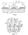
- Figure 1 sets forth a preferred embodiment of the latter wherein a magnetostrictive film is deposited over a piezoresistively responsive region associated with the gate area of a MOSFET transistor.
- the device 10 includes a substrate 12 of P-type silicon in which two zones have been heavily doped to provide N-type regions 14 and 16, respectively.
- insulating Si0 2 regions 18, 20, and 22, respectively On top of the substrate and adjoining the N-type regions 14 and 16 are formed insulating Si0 2 regions 18, 20, and 22, respectively, and on top of the regions 18 and 22 are deposited metallic contact regions 24 and 26 respectively.
- a metallic magnetostrictive film 28 is then deposited, thus completing a modified MOSFET transistor.
- the Si substrate, particularly in channel area 31 is appropriately strain sensitive, i.e.
- Appropriate bias potentials such as provided by sources 30 and 32 may be applied to the device via conductors 34, 36, and 38 secured to the contacts 24, 26, and 28, respectively, and an output signal developed across resistor 40.
- a device such as that set forth in Figure 1 was constructed in the following manner.
- a P-channel enhancement mode MOSFET transistor was fabricated from an N-type silicon substrate utilizing conventional MOSFET technology, wherein the gate electrode was prepared having dimensions of approximately 25 by 1,000 micrometers.
- a magnetostrictive thin film approximately 500 nanometers thick was ion beam sputtered onto the gate electrode from a 98%+ pure nickel foil target.
- other magnetostrictive thin films may also be deposited, such as an alloy of approximately Fe, o Si 3o .
- Equivalent devices to that shown in Figure 1 may be made using either N-channel or P-channel silicon substrates, operating in either an enhancement or depletion mode. Also, analogous devices may be constructed using bipolar transistors.
- an alternative device may utilize a totally passive substrate, such as formed of a planar sheet of glass or the like, onto which is then adhered a conventional MOSFET transistor having the respective doped regions, insulating layers, and metallic contacts, as described hereinabove with respect to the MOSFET of the device 10 and set forth in Figure 1.
- a second portion of the device consisting of a substrate and a magnetically activated piezoresistor, formed by first depositing a piezoresistive film. Suitable electrical contacts are applied to two sides of the film.
- an insulating thin film such as Si0 2
- a thin film of a magnetostrictive material such as Ni.
- Appropriate electrical contacts are then provided to couple the piezoresistor and bias potentials to the MOSFET transistor.
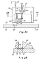
- a device functionally equivalent to that described in conjunction with Figure 1 hereinabove may be constructed by adding suitable high permeability pole pieces to enable remote sensing of localized magnetic fields such as may be present in magnetic recording media.
- One such device is set forth in plane view in Figure 2A, and associatedly, in cross-section view in Figure 2B.
- the device 90 includes a silicon substrate 92 having a region 94 having appreciable piezoresistive characteristics. At opposite ends of the region 94 are deposited electrodes 96 and 98. Overlying the piezoresistive region 94 is a thin film insulator 100 and overlying the insulating thin film 100 is a thin film of a magnetostrictive material 102.
- the pole piece 106 is desirably made sufficiently extensive in area to result in a flux density sufficiently low to avoid magnetically affecting recorded data passing adjacent that pole piece.
- the flux thus induced in the magnetostrictive film 102 will produce an associated electrical output from the piezoresistive region.
- a conventional bipolar transistor 116 is separately fabricated and bonded to the silicon substrate 92 as there shown.
- the electrodes 96 and 98 may then be coupled between a source of potential 120 and the base 122 of the transistor. 116.
- the collector and emitter 124 and 126, respectively, can be coupled via leads 128 and 130 to an appropriate bias circuit.
- such a device includes the substrate 92 having a piezoresistive region 94.
- the metal electrodes 96 and 98 On top of the region 94 are the metal electrodes 96 and 98, the insulating film 100 and the magnetostrictive film 102, respectively.
- the high permeability thin film pole pieces 104 and 106 are similarly shown deposited over the magnetostrictive film, leaving the gap region therebetween.
- An alternative construction may provide the capability to read both longitudinally and perpendicularly recorded data.
- Such a device utilizes symmetric, thin film pole pieces deposited over a magnetostrictive-piezoresistive transducer substantially the same as that shown in Fig. 2A.
- One pole piece would thus terminate with an underlying pole tip substantially covered by a second pole tip, the two pole tips being separated by an insulative thin film, thus forming the working gap of the resultant head.
- the construction of such thin film heads is well known to those skilled in thin film recording and playback head technology.
- the present invention may also be utilized with external pole pieces to provide both a read and write capability.
- a device may include a silicon substrate on which are deposited successive thin films so as to form a single turn inductive winding around the appropriate pole pieces together with a magnetostrictive-piezoresistive transducer assembly as described above.
- Figure 3 sets forth in perspective view a further preferred embodiment of the present invention wherein a plurality of magnetostrictive-piezoresistive sensing elements are provided, thus enabling simultaneous playback of parallel tracks.
- a device may also be used to maintain the head positioned over a single track via a dynamic servoing system.
- a head 182 may include a silicon substrate 184 into which is diffused a plurality of piezoresistively responsive regions 186, 188 and 190, into the ends of which are formed highly conductive regions 192 and 194, 196 and 198, and 200 and 202, respectively.
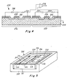
- FIG. 4 sets forth a preferred embodiment of the present invention wherein additional components are provided for suppressing unwanted effects of stimuli other than the main magnetic signals of interest.
- a pair of sensing elements as nearly geometrically identical as possible are provided, with only one of the sensing elements receiving the stimuli of interest, but with both the sensing elements equally receiving all background stimuli.
- the device set forth in Figure 4 incorporates a common mode noise rejection feature.
- the device 232 includes a common substrate 234 within which are fabricated two separate MOSFET transistors each shown generally extending over two separate regions 236 and 238, respectively, of the substrate.
- MOSFET transistors are conventional in nature so far as having the requisite doped regions, metal oxide layers and source, gate, and drain electrodes, but further modified to have piezoresistively responsive channels.
- the common mode noise rejection capability is provided by depositing over the respective gate regions 240 and 242 a magnetostrictive film 244 and a similarly configured non-magnetostrictive film 246, such as may be provided by a thin film of aluminum, or the like.
- each of the respective films 244 and 246 may be provided to allow applications of appropriate bias potentials.
- Appropriate sources of potential and biasing resistors, 248 and 250, and 252 and 254, respectively, will also be provided for energization of the two separate MOSFET sections.
- the output from the two respective MOSFET sections will then typically be coupled to a differential amplifier 256 to provide an appropriate differential output signal.
- common mode noise rejection may be obtained even though both the films 244 and 246 are magnetostrictive in nature.
- only one of the films would be exposed to the desired magnetic field, with appropriate shielding provided if desired to minimize cross-talk.
- the difference between the outputs of the two would represent a magnetically induced signal with common mode noise rejected.
- common mode noise rejection may similarly be achieved using a single MOSFET device.
- a single MOSFET device can be fabricated using a single silicon substrate, upon a first portion of which is fabricated a conventional MOSFET transistor.
- a single piezoresistive zone is then formed, having separated, highly conductive regions of equal resistance. Overlying one half of the piezoresistive zone would then be provided an insulating layer, and on top of that layer would be provided a magnetostrictive layer. Analogously, overlying the other half of the piezoresistive zone would be another insulating layer and on top of that layer would be a non-magnetostrictive layer.
- the two piezoresistors thus formed, in combination with a source of potential, constitute a biasing network for the MOSFET.
- Application of an external magnetic field thus modulates the resistance of the zone underlying the magnetostrictive layer, and results in a change in the bias potential applied to the MOSFET.
- one such device 304 includes a conventional ceramic chip carrier 306 which is arranged to have an internal recess and to be open at one end 308.
- chip carriers typically have a plurality of bonding pads positioned about their periphery for enabling electrical connections to be made to the various portions of a semiconductor substrate positioned therein.
- a silicon substrate 310 is mounted within the carrier 306 using an appropriate thermally conductive adhesive, with one end of the substrate terminating substantially coincident with the open end of the carrier 308.
- a magnetostrictive film 314 and a non-magnetostrictive film 316 are deposited over an insulating film 318 covering separate piezoresistive zones 320 and 322.
- the magnetostrictive film is a thin film of an iron-silicon alloy having the approximate composition Fe 7o SJ 3o with a thickness in the range of 20G-800 nanometers.
- the non-magnetostrictive film 316 may be a sputtered film of aluminum having a thickness of approximately 300 to 500 nanometers, and of similar physical dimensions.
- the differently fabricated piezoresistors may be coupled to the electrodes of integrated transistors 328 and 330, bonded to another portion of the substrate 310 via a suitable thermally conductive adhesive, or fabricated as an integral portion thereof.
- the periphery of the chip carrier 306 will include bonding pads (not shown) so that connections to appropriate biasing potentials and input and/or output signals may be made to the transistors.
- a chip carrier such as described in the foregoing, having the respective films terminating proximate the open end of the carrier, may be utilized to detect perpendicularly encoded localized magnetic field patterns within a magnetic recording medium.
- a medium may include a layer of a vertically oriented magnetic recording material over a high permeability substrate, which thereby provides an efficient flux return path. As such a medium is moved past the carrier, localized bits will come proximate the magnetostrictive and metallic films, and differential strain will be induced within the magnetostrictive film 314 to provide an appropriate signal from the transistors.
- the amplifier which desirably forms an integrated part of the device of the present invention may be a MOSFET, JFET or bipolar type transistor and thus provides the first stage of amplification as well as impedance matching, to the magnetostrictive-piezoresistive portion of the device.
- the transistors desirably used in the present devices can be fabricated by standard IC processes.
- the device of the present invention can be fabricated with MOSFET amplifiers employing either N-type or P-type channels, operating in either the enhancement or depletion mode.
- magnetostrictive stratum such a layer is desirably deposited in intimate mechanical contact with the piezoresistive stratum.
- magnetostrictive elements include various compositions of FeSi, FeB, Ni, FeSiTb, FeNi, etc.
- Optimum thicknesses and application techniques will depend upon the particular material selected. There are a variety of techniques available to provide for coupling between the magnetostrictive and piezoresistive strata.
- the magnetostrictive material may be sputtered, evaporated, plated, or even adhered with, for example, a thin epoxy layer over the piezoresistive material.
- the mechanical and electrical characteristics of the device will depend on the particular deposition or application method employed.
- magnetostrictive film that actually couples to a magnetic field. Consequently, it properties are perhaps the most critical to device performance.
- the basic material characteristics required are relatively low coercivity, so that the film magnetization can be easily switched, and a relatively high magnetostriction coefficient.
- the particular properties of the magnetostrictive layer can be tailored somewhat to match the properties of the piezoresistive stratum and amplifier being used. However, in general it is desirable to have the highest possible induced strain per unit applied field, consistent with achieving magnetic saturation in digital applications at an acceptably low field intensity.
- the physical dimensions of the film determine the spatial field resolution and bandwidth of the sensor. Thin film, photolithographically patterned elements can achieve maximum bandwidth and resolution.
Landscapes
- Engineering & Computer Science (AREA)
- Manufacturing & Machinery (AREA)
- Physics & Mathematics (AREA)
- Condensed Matter Physics & Semiconductors (AREA)
- General Physics & Mathematics (AREA)
- Magnetic Heads (AREA)
- Measuring Magnetic Variables (AREA)
- Hall/Mr Elements (AREA)
Claims (11)
daß der Verstärker Mittel (252, 254 und 256) aufweist, die dazu dienen, Veränderungen des spezifischen elektrischen Widerstandes der zweiten Piezowiderstandsschicht (238) zu erfassen und auf Grund derselben ein zweites Ausgangssignal abzugeben, das auf den Bereich der genannten anderen Schicht winwirkenden Reizen entspricht.
Priority Applications (1)
| Application Number | Priority Date | Filing Date | Title |
|---|---|---|---|
| AT83303179T ATE42413T1 (de) | 1982-07-14 | 1983-06-02 | Magnetischer sensor, insbesondere wiedergabekopf fuer magnetisches aufzeichnungsmedium. |
Applications Claiming Priority (2)
| Application Number | Priority Date | Filing Date | Title |
|---|---|---|---|
| US06/398,419 US4499515A (en) | 1982-07-14 | 1982-07-14 | Integrated magnetostrictive-piezoresistive magnetic recording playback head |
| US398419 | 1982-07-14 |
Publications (3)
| Publication Number | Publication Date |
|---|---|
| EP0103352A2 EP0103352A2 (de) | 1984-03-21 |
| EP0103352A3 EP0103352A3 (en) | 1985-10-23 |
| EP0103352B1 true EP0103352B1 (de) | 1989-04-19 |
Family
ID=23575311
Family Applications (1)
| Application Number | Title | Priority Date | Filing Date |
|---|---|---|---|
| EP83303179A Expired EP0103352B1 (de) | 1982-07-14 | 1983-06-02 | Magnetischer Sensor, insbesondere Wiedergabekopf für magnetisches Aufzeichnungsmedium |
Country Status (9)
| Country | Link |
|---|---|
| US (1) | US4499515A (de) |
| EP (1) | EP0103352B1 (de) |
| JP (1) | JPS5924426A (de) |
| KR (1) | KR940004988B1 (de) |
| AT (1) | ATE42413T1 (de) |
| CA (1) | CA1196093A (de) |
| DE (1) | DE3379678D1 (de) |
| HK (1) | HK89889A (de) |
| SG (1) | SG59489G (de) |
Families Citing this family (22)
| Publication number | Priority date | Publication date | Assignee | Title |
|---|---|---|---|---|
| CH659896A5 (de) * | 1982-11-22 | 1987-02-27 | Landis & Gyr Ag | Magnetfeldsensor. |
| US4604669A (en) * | 1984-09-04 | 1986-08-05 | Honeywell Inc. | Magnetostrictive record head |
| WO1989006733A1 (en) * | 1988-01-20 | 1989-07-27 | Widén Innovation Ab | Cylinder lock and locking tumbler |
| US4918655A (en) * | 1988-02-29 | 1990-04-17 | Honeywell Inc. | Magnetic device integrated circuit interconnection system |
| US5262666A (en) * | 1989-05-15 | 1993-11-16 | Nippondenso Co., Ltd. | Semiconductor device with a nickel alloy protective resistor |
| US5229621A (en) * | 1989-11-15 | 1993-07-20 | Hitachi, Ltd. | Magnetic semiconductor element and a magneto-optical read out head |
| US5992601A (en) * | 1996-02-15 | 1999-11-30 | Cummins-Allison Corp. | Method and apparatus for document identification and authentication |
| DE69117634T2 (de) * | 1990-09-28 | 1996-10-24 | Sony Corp | Magnetkopf mit dem Effekt der Widerstandsänderung im Magnetfeld |
| US5633092A (en) * | 1991-12-10 | 1997-05-27 | British Technology Group Ltd. | Magnetostrictive material |
| GB9126207D0 (en) * | 1991-12-10 | 1992-02-12 | Nat Res Dev | Magnetostrictive material |
| US5476691A (en) * | 1994-01-21 | 1995-12-19 | International Business Machines, Inc. | Surface treatment of magnetic recording heads |
| AU1563995A (en) * | 1994-01-21 | 1995-08-08 | Regents Of The University Of California, The | Surface treatment of ceramic articles |
| US5680280A (en) * | 1995-09-11 | 1997-10-21 | Texas Instruments Incorporated | Magnetic field sensor using heterojunction bipolar transistors |
| KR0176237B1 (ko) * | 1995-12-08 | 1999-03-20 | 양승택 | 박막 트랜지스터 및 그의 제조방법 |
| US6809515B1 (en) | 1998-07-31 | 2004-10-26 | Spinix Corporation | Passive solid-state magnetic field sensors and applications therefor |
| WO2000060369A1 (en) * | 1999-04-05 | 2000-10-12 | Spinix Corporation | Passive solid-state magnetic field sensors and applications therefor |
| US6580271B2 (en) * | 1999-07-20 | 2003-06-17 | Spinix Corporation | Magnetic field sensors |
| US7059201B2 (en) * | 2000-12-20 | 2006-06-13 | Fidelica Microsystems, Inc. | Use of multi-layer thin films as stress sensors |
| KR100773556B1 (ko) * | 2006-08-02 | 2007-11-07 | 삼성전자주식회사 | 전계 재생/기록 헤드와 그의 제조방법 및 전계 재생/기록헤드를 포함한 정보 재생/기록 장치 |
| US7948713B2 (en) * | 2007-01-12 | 2011-05-24 | Tdk Corporation | Magnetic head slider using giant magnetostrictive material |
| WO2010006284A1 (en) * | 2008-07-11 | 2010-01-14 | Brain Basket, LLC | Magnetostrictive auditory system |
| WO2013052846A1 (en) | 2011-10-06 | 2013-04-11 | Brain Basket, LLC | Auditory comprehension and audibility device |
Family Cites Families (9)
| Publication number | Priority date | Publication date | Assignee | Title |
|---|---|---|---|---|
| US3344237A (en) * | 1967-09-26 | Desposited film transducing apparatus and method op producing the apparatus | ||
| FR1054802A (de) * | 1951-01-24 | 1954-02-15 | ||
| JPS5332690B2 (de) * | 1972-06-13 | 1978-09-09 | ||
| US3800193A (en) * | 1972-09-05 | 1974-03-26 | Ibm | Magnetic sensing device |
| US3987485A (en) * | 1973-02-20 | 1976-10-19 | Matsushita Electric Industrial Co., Ltd. | Magnetic head with thin film components |
| US3909809A (en) * | 1973-12-17 | 1975-09-30 | Canadian Patents Dev | Magnetic bubble domain sensing device |
| US3908194A (en) * | 1974-08-19 | 1975-09-23 | Ibm | Integrated magnetoresistive read, inductive write, batch fabricated magnetic head |
| US4129880A (en) * | 1977-07-01 | 1978-12-12 | International Business Machines Incorporated | Channel depletion boundary modulation magnetic field sensor |
| US4520413A (en) * | 1982-04-13 | 1985-05-28 | Minnesota Mining And Manufacturing Company | Integrated magnetostrictive-piezoelectric-metal oxide semiconductor magnetic playback head |
-
1982
- 1982-07-14 US US06/398,419 patent/US4499515A/en not_active Expired - Fee Related
-
1983
- 1983-04-27 CA CA000426797A patent/CA1196093A/en not_active Expired
- 1983-06-02 EP EP83303179A patent/EP0103352B1/de not_active Expired
- 1983-06-02 AT AT83303179T patent/ATE42413T1/de not_active IP Right Cessation
- 1983-06-02 DE DE8383303179T patent/DE3379678D1/de not_active Expired
- 1983-07-13 JP JP58126298A patent/JPS5924426A/ja active Pending
- 1983-07-14 KR KR1019830003217A patent/KR940004988B1/ko not_active Expired - Fee Related
-
1989
- 1989-09-06 SG SG594/89A patent/SG59489G/en unknown
- 1989-11-09 HK HK898/89A patent/HK89889A/en not_active IP Right Cessation
Also Published As
| Publication number | Publication date |
|---|---|
| EP0103352A2 (de) | 1984-03-21 |
| JPS5924426A (ja) | 1984-02-08 |
| DE3379678D1 (en) | 1989-05-24 |
| KR940004988B1 (ko) | 1994-06-09 |
| KR840005584A (ko) | 1984-11-14 |
| SG59489G (en) | 1989-12-29 |
| US4499515A (en) | 1985-02-12 |
| CA1196093A (en) | 1985-10-29 |
| ATE42413T1 (de) | 1989-05-15 |
| EP0103352A3 (en) | 1985-10-23 |
| HK89889A (en) | 1989-11-17 |
Similar Documents
| Publication | Publication Date | Title |
|---|---|---|
| EP0103352B1 (de) | Magnetischer Sensor, insbesondere Wiedergabekopf für magnetisches Aufzeichnungsmedium | |
| US4520413A (en) | Integrated magnetostrictive-piezoelectric-metal oxide semiconductor magnetic playback head | |
| US5255141A (en) | Read-write magnetic head with flux sensing read element | |
| US3860965A (en) | Magnetoresistive read head assembly having matched elements for common mode rejection | |
| US5218497A (en) | Magnetic recording-reproducing apparatus and magnetoresistive head having two or more magnetoresistive films for use therewith | |
| EP0484474B1 (de) | Hochdichte signalverstärkung zeigender magnetoresistiver wiedergabekopf mit kurzgeschlossenem doppelelement | |
| KR100260804B1 (ko) | 박막 자기 헤드 | |
| JPS63117309A (ja) | 磁気抵抗性読取変換器 | |
| JPS63255809A (ja) | 狭いトラックに対する読取磁気ヘッド及びその製造方法 | |
| JPH0473201B2 (de) | ||
| EP0675486A2 (de) | Magnetoresistiver Wandler mit integriertem Joch und magnetischem Nebenschluss | |
| US4432028A (en) | Shielded magnetoresistance transducer high data density applications | |
| JP2002100009A (ja) | 磁気抵抗効果型磁気ヘッド | |
| US5905610A (en) | Combined read/write magnetic head having MRE positioned between broken flux guide and non-magnetic substrate | |
| JPS61120318A (ja) | 一体化薄膜磁気ヘツド | |
| US6028749A (en) | Magnetic head having a multilayer structure and method of manufacturing the magnetic head | |
| JP3285094B2 (ja) | 薄膜磁気ヘッドの研磨方法 | |
| JPH0115927B2 (de) | ||
| JPS58224430A (ja) | 混成薄膜集積ヘツド | |
| JPH028468B2 (de) | ||
| JPS61248213A (ja) | 薄膜磁気ヘツド | |
| JPS62197909A (ja) | 磁気ヘツドおよびその製造方法 | |
| JPS61908A (ja) | 磁気抵抗効果型再生ヘツド | |
| JPH07262528A (ja) | 薄膜水平型読出し磁気ヘッド | |
| JPH1083518A (ja) | 磁気抵抗効果型磁気ヘッド |
Legal Events
| Date | Code | Title | Description |
|---|---|---|---|
| PUAI | Public reference made under article 153(3) epc to a published international application that has entered the european phase |
Free format text: ORIGINAL CODE: 0009012 |
|
| AK | Designated contracting states |
Designated state(s): AT DE FR GB IT NL |
|
| PUAL | Search report despatched |
Free format text: ORIGINAL CODE: 0009013 |
|
| AK | Designated contracting states |
Designated state(s): AT DE FR GB IT NL |
|
| 17P | Request for examination filed |
Effective date: 19860325 |
|
| 17Q | First examination report despatched |
Effective date: 19870723 |
|
| ITF | It: translation for a ep patent filed | ||
| GRAA | (expected) grant |
Free format text: ORIGINAL CODE: 0009210 |
|
| AK | Designated contracting states |
Kind code of ref document: B1 Designated state(s): AT DE FR GB IT NL |
|
| REF | Corresponds to: |
Ref document number: 42413 Country of ref document: AT Date of ref document: 19890515 Kind code of ref document: T |
|
| REF | Corresponds to: |
Ref document number: 3379678 Country of ref document: DE Date of ref document: 19890524 |
|
| ET | Fr: translation filed | ||
| PLBE | No opposition filed within time limit |
Free format text: ORIGINAL CODE: 0009261 |
|
| STAA | Information on the status of an ep patent application or granted ep patent |
Free format text: STATUS: NO OPPOSITION FILED WITHIN TIME LIMIT |
|
| 26N | No opposition filed | ||
| ITTA | It: last paid annual fee | ||
| PGFP | Annual fee paid to national office [announced via postgrant information from national office to epo] |
Ref country code: NL Payment date: 19970331 Year of fee payment: 15 |
|
| PGFP | Annual fee paid to national office [announced via postgrant information from national office to epo] |
Ref country code: GB Payment date: 19970506 Year of fee payment: 15 |
|
| PGFP | Annual fee paid to national office [announced via postgrant information from national office to epo] |
Ref country code: AT Payment date: 19970523 Year of fee payment: 15 |
|
| PGFP | Annual fee paid to national office [announced via postgrant information from national office to epo] |
Ref country code: FR Payment date: 19970610 Year of fee payment: 15 |
|
| PGFP | Annual fee paid to national office [announced via postgrant information from national office to epo] |
Ref country code: DE Payment date: 19970627 Year of fee payment: 15 |
|
| PG25 | Lapsed in a contracting state [announced via postgrant information from national office to epo] |
Ref country code: GB Free format text: LAPSE BECAUSE OF NON-PAYMENT OF DUE FEES Effective date: 19980602 Ref country code: AT Free format text: LAPSE BECAUSE OF NON-PAYMENT OF DUE FEES Effective date: 19980602 |
|
| PG25 | Lapsed in a contracting state [announced via postgrant information from national office to epo] |
Ref country code: NL Free format text: LAPSE BECAUSE OF NON-PAYMENT OF DUE FEES Effective date: 19990101 |
|
| GBPC | Gb: european patent ceased through non-payment of renewal fee |
Effective date: 19980602 |
|
| PG25 | Lapsed in a contracting state [announced via postgrant information from national office to epo] |
Ref country code: FR Free format text: LAPSE BECAUSE OF NON-PAYMENT OF DUE FEES Effective date: 19990226 |
|
| NLV4 | Nl: lapsed or anulled due to non-payment of the annual fee |
Effective date: 19990101 |
|
| PG25 | Lapsed in a contracting state [announced via postgrant information from national office to epo] |
Ref country code: DE Free format text: LAPSE BECAUSE OF NON-PAYMENT OF DUE FEES Effective date: 19990401 |
|
| REG | Reference to a national code |
Ref country code: FR Ref legal event code: ST |