EP0100737A2 - Freigabegatter für drei Zustände mit Schwellschaltung zur Aktivierung der Speisespannung - Google Patents
Freigabegatter für drei Zustände mit Schwellschaltung zur Aktivierung der Speisespannung Download PDFInfo
- Publication number
- EP0100737A2 EP0100737A2 EP83401593A EP83401593A EP0100737A2 EP 0100737 A2 EP0100737 A2 EP 0100737A2 EP 83401593 A EP83401593 A EP 83401593A EP 83401593 A EP83401593 A EP 83401593A EP 0100737 A2 EP0100737 A2 EP 0100737A2
- Authority
- EP
- European Patent Office
- Prior art keywords
- threshold
- circuit
- power supply
- transistor
- coupled
- Prior art date
- Legal status (The legal status is an assumption and is not a legal conclusion. Google has not performed a legal analysis and makes no representation as to the accuracy of the status listed.)
- Granted
Links
Images


Classifications
-
- H—ELECTRICITY
- H03—ELECTRONIC CIRCUITRY
- H03K—PULSE TECHNIQUE
- H03K19/00—Logic circuits, i.e. having at least two inputs acting on one output; Inverting circuits
- H03K19/02—Logic circuits, i.e. having at least two inputs acting on one output; Inverting circuits using specified components
- H03K19/08—Logic circuits, i.e. having at least two inputs acting on one output; Inverting circuits using specified components using semiconductor devices
- H03K19/082—Logic circuits, i.e. having at least two inputs acting on one output; Inverting circuits using specified components using semiconductor devices using bipolar transistors
- H03K19/0823—Multistate logic
- H03K19/0826—Multistate logic one of the states being the high impedance or floating state
-
- H—ELECTRICITY
- H03—ELECTRONIC CIRCUITRY
- H03K—PULSE TECHNIQUE
- H03K17/00—Electronic switching or gating, i.e. not by contact-making and –breaking
- H03K17/22—Modifications for ensuring a predetermined initial state when the supply voltage has been applied
-
- H—ELECTRICITY
- H03—ELECTRONIC CIRCUITRY
- H03K—PULSE TECHNIQUE
- H03K17/00—Electronic switching or gating, i.e. not by contact-making and –breaking
- H03K17/22—Modifications for ensuring a predetermined initial state when the supply voltage has been applied
- H03K2017/226—Modifications for ensuring a predetermined initial state when the supply voltage has been applied in bipolar transistor switches
Definitions
- the present invention relates to a new power supply threshold activation circuit for sequencing the turn on and turn off of multiple circuit devices or subcircuits dependent on a common power supply.
- the invention is particularly applicable in tristate enable circuits for maintaining the high Z or high impedance third state of a common bus tristate output device during power down, power up, and power out trans.itions of the common power supply. More generally the invention is useful in any application where a portion of circuitry must be kept active or for introducing a backup power supply during power transitions or power outages of the conventional power supply.
- FIG. 1 a-prior art Fairchild Advanced Schottky TTL three state or tristate-output control device is illustrated in Figure 1.
- the pullup element for sourcing current from the higher level voltage and power supply V cc consists of transistors Q12 and Q13 forming a Darlington.current source.
- the Darlington current source supplies current from power supply V cc to the output V out .
- the "pulldown" element or stage for sinking current and voltage from the output V out to ground consists of transistor Q14 with a conventional squaring network including transistor Q16 at its base.
- the pulldown transistor Q14 also includes a turn off accelerating transistor Q15 and associated diodes for sinking Miller current and accelerating turn off of pull down transistor Q14 during transition from low to high at the output V out .
- Step up transistor Q10 is coupled in series with the phase splitter Qll to increase the input threshold at the logic data input V in .
- the third state or high impedance state of the tristate device illustrated in Figure 1 is afforded by the output enable terminal OE.
- the output enable terminal OE When a low level potential or binary zero from the enable gate appears at terminal OE the active elements of the tristate device are deprived of base drive current.
- terminal OE provides a low impedance path to ground and all transistors become nonconducting.
- both the pullup element and-pulldown element exhibit high impedance to signals appearing at the output V out . With all the elements deprived of base current the output effectively becomes a high impedance to any exterior.circuitry, for example, a common bus to which the output V out may be connected.
- the tristate output device will neither source nor-sink current at the output V out and will behave effectively as if nothing were-there.
- Such a tristate device is therefore particularly applicable and suitable for applications in which a plurality of output gates are tied together or coupled to a common bus structure.
- common bus applications only one output, that is only one of many output devices of the type illustrated in Figure 1 coupled to the bus structure, determines the voltage (high or low) of the bus while the other outputs for the remaining gates are in the high impedance third state.
- the output device When a high level voltage binary one appears at the output enable terminal OE the output device functions as a bistate output device sinking or sourcing current at the output V out according to whether the pulldown or pullup element is conducting. It should be noted that the output device is inherently inverting as a binary zero at the input V in generates a binary one at the output V out and vice versa. As stated above only one such tristate output device of many coupled to the common bus is active at any one time.
- the enable gate which delivers a high or low voltage signal, binary one or zero, to the output enable terminal OE is itself a bistate TTL gate.
- the enable gate In order to relinquish the common bus, not shown, to another tristate output device which is actively passing logic data in a bistate mode, the enable gate must remain actively conducting through its own pulldown element.
- the enable gate pulldown element affords a low impedance path from the output enable terminal OE to ground, continuously sinking base current from the transistors of the tristate output device. It is essential that the enable gate remain continuously activated for sinking-current in order to maintain the high impedance or high Z state and prevent interference with high and low signals on the bus.
- the pulldown element Q14 affords a low impedance path to ground at the tristate output V out and therefore at the entire common bus affecting all other devices connected to the bus. The system reliability is therefore. reduced during power down and power up voltage transitions at the power supply V cc .
- a threshold. type circuit for detecting a drop in the:system power supply voltage and for turning off bias networks in a sequence making it impossible to write into or change the data in a memory cell. The memory cells are thus protected while the power supply voltage is reduced to the minimum cell current requirements for maintaining the cell contents.
- Threshahd activation and control.circuits and concepts have never been applied however to the unique requirements of tristate output devices and their associated enable gate circuits. More generally, such threshold circuits and concepts have not been applied to interdependent logic gate output circuits and subcircuits. Nor would the threshold detecting circuit of U.S. Patent 4,104,734 be of a type that could optimally be applied in such environments all as hereafter described.
- Another object of the invention is to provide new enable gate-circuits for sequencing the turn off or deactivation and turn on of circuit elements during power down and power up transitions of the common power supply so that.spurious loss of high impedance coupling of the inactive devices at a common bus may not occur.
- the present invention contemplates providing an improved tristate enable circuit-for activating a tristate enable gate to maintain the high impedance third state of a common bus tristate device during power down and power up transitions of the common power supply V cc . This is true even when the enable-gate circuit elements normally turn off at a higher voltage level V cc2 than the lower-voltage leue V cc3 at which the circuit elements of the common bus tristate device turn off. Thus, spurious introduction of high and low voltage signals at the common bus is avoided.
- the invention provides a threshold activation circuit coupled to the enable gate for activating the enable gate when the threshold activation circuit senses a common power supply voltage level Vccl.
- the threshold activation circuit is designed for operatively activating the enable gate over a voltage range from Vccl to a lesser common power supply voltage level V cc4 .
- the threshold activation circuit component values are selected for operatively relating the voltage levels so that V cc1 > V cc2 and V cc3 > V cc4 .
- a feature and advantage of this circuit selection is that the turn off of circuit elements is sequenced by the threshold activation circuit in the desired order.
- the threshold activation circuit comprises a threshold transistor and a threshold ladder circuit coupled to the terminals of the threshold transistor. 'The output of the threshold activation circuit is.coupled through an inverting transistor to the enable gate pulldown element in parallel with the enable gate phase splitter.
- the threshold activation circuit however continues to drive the pulldown element of the enable gate providing a low impedance path to ground which continues to deprive the tristate output device of base drive current.
- the tristate output device seeing a low level potential or binary zero at the output enable terminal OE remains in the high Z state. Without the threshold activation circuit in accordance with the invention a high impedance would appear at terminal OE upon deactivation or turn-off of the enable gate. As a result, the tristate output device may interfere with data passing on the bus from another device in the active bistate mode.
- V cc3 As the power down or power loss continues a voltage level V cc3 is reached at which the tristate output device itself becomes deactivated and its active element transistors are no longer conducting. Below this voltage level spurious results on the common bus can no longer occur. Therefore, at a final lower voltage level V cc4 the threshold activation circuit itself turns off. This sequence takes place in reverse during power up transitions of the power supply so that spurious voltage levels on the common bus are eliminated during transitions in either direction according to the present invention.
- the threshold ladder circuit may take a number of forms but includes as basic elements at least a collector resistor coupled between the collector of the threshold transistor and the power supply; clamping devices such as diodes, and a base supply resistor coupled in series between the base of the threshold transistor and power supply; and a base to ground resistor coupled between the base of the threshold resistor and ground or low level potential.
- the output from the threshold activation circuit is taken from the collector of the threshold transistor through a coupling gate such a diode or active element transistor according to the application.
- a pass transistor inverter is used for coupling the threshold transistor to .the enable gate pulldown element transistor while inverting the voltage signal.
- the threshold activation circuit is applicable for sequencing the activation or turn off of interdependent multiple circuit devices or subcircuits during power down, power up, and power out transitions of the common power supply.
- the threshold activation circuit is used to control introduction of a separate or independent backup power supply, for example, into a memory board or other application where active subcircuits must be maintained during power down transitions or unintentional power losses.
- a tristate enable circuit modified in accordance with the present-invention is illustrated in Figure 2. Such an enable circuit is suitable for controlling tristate output devices of the type described above with reference to Eigure 1.
- the enable circuit also referred to as an enable gate is itself a TTL device.
- the primary operative element of the enable gate is the active element pulldown transistor Q7 which sinks current from the output QE of the enable gate when conducting.
- the puIlug element transistors Q5 and Q6 forming a Darlington are nonconducting and a binary zero or low potential appears at the output OE affording a low impedance path to.ground from the collector to emitter of pulldown transistor Q7.
- the enable gate controls or holds-an associated tristate output device in the high impedance or high Z third state.
- phase splitter transistor Q4 and stepup transistor Q3 which increases the threshold voltage at the enable gate input OE for switching the enable gate.
- the logic circuits illustrated in Figures 1 and 2 are typically incorporated in integrated circuits using any of a number of technologies, for example, MOS, CMOS, ECL, and Fairchild Advanced-Schottky TTL (FAST) technologies.
- the invention is also applicable to discrete component circuits.
- enable gate With enable gate pulldown transistor Q7 nonconducting, an interval of time therefore exists before turn off of the tristate output device when the output device is no longer held in the high-Z state.
- spurious signals may appear on the common bus interfering in the transfer of data from another output device, then in the active bistate mode.
- the pulldown element of the tristate output device may become conducting pulling the common bus down to ground or low potentials
- the invention incorporates a novel threshold activation circuit 20 as an integral part of the enable circuit.
- the threshold activation circuit includes an active element threshold transistor Ql with circuit components coupled at its terminals between the high level power voltage V cc and low level ground potential or ground, in the form of a "threshold ladder" circuit.
- collector resistor R3 connects the collector of transistor Ql to power supply V cc .
- Clamping devices in this instant diodes Dl and D2 in series with base supply resistor Rl connect the base of transistor Ql to the common power supply V cc .
- the base to ground resistor R2 connects the base of transistor Ql to ground or low level potential and the emitter of transistor Ql is also connected to ground potential.
- the purpose of threshold activation circuit 20 is to sense a transition in the power supply voltage V cc and take corrective or preventive action to prevent the enable gate pulldown transistor Q7 from turning off before the tristate output device.
- V cc is high enough to keep threshold transistor Ql conducting.
- threshold transistor Ql With threshold transistor Ql conducting the coupling gate transistor Q2.according to the invention is deprived of base drive current and remains off.
- Transistor Q2 is a pass transistor inverter used to interface or couple the threshold activation circuit 20 to the enable gate and is particularly suited for that purpose. In other applications a coupling gate other than a transistor, for example, a diode may be used.
- Transistor inverter Q2 is required for controlling the pulldown transistor Q7 of the enable gate.
- Transistor inverter Q2 is coupled with its collector and emitter in parallel with the enable gate phase splitter transistar Q4 and in this position is able to control and drive the pulldown transistor Q7 in the event the phase splitter transistor Q4 turns off.
- V cc1 As power supply V cc is reduced a threshold V cc1 is reached where Q1 will no longer.conduct.
- This voltage threshold is given approximately by the following equation: where V D1 and V D2 are the voltage drops across diodes Dl and D2 respectively and VBE Q1 is the voltage drop across the base to emitter junction of threshold transistor Ql.
- This voltage threshold V ccl may be adjusted by appropriate values for Rl and R2, and the number of clamping devices, in this instance diodes.
- At voltage levels below the threshold V cc1' threshold transistor Ql turns off and inverter transistor Q2 turns on as a result of base drive current through resistor R3.
- the coupling transistor Q2 in turn supplies base drive current to the enable gate pulldown transistor Q7 holding it on in the conducting state.
- the emitter to collector low impedance conducting path of transistor Q2 holds the Darlington consisting of transistors Q5 and Q6 off and nonconducting.
- the enable gate phase splitter transistor Q4 and the threshold.activation circuit coupling transistor Q2 thus cooperate in parallel to maintain a high Z or high impedance third state in the associated tristate output device connected to terminal OE.
- V cc2 As the power supply V cc continues in a downward or power down transition, there is a point V cc2 where phase splitter transistor Q4 shuts off. This is given approximately by the following equation: where.VBE is the voltage drop across the base to emitter junction and VSAT is the voltage drop across the collector to emitter junction of the transistor in saturation.
- the enable gate circuit elements and in particular the phase splitter transistor Q4 turns off during a downward transition of the power supply V cc before the elements of the tristate output device.
- the circuit component values are selected so that V cc1 > V cc2 .
- the turn off level for tristate output device pulldown transistor Q14 is a function of the voltage drop, VBE, across the base emitter junctions of transistors Q10, Qll and Q14 and is also a function of the various resistors R10, Rll, R12, R14 and R15.
- the turn off of the Darlington is a function of VBE across transistors Q12 and Q13 along with other circuit components including resistors R11 and R17.
- V cc3 is -also a function of the potentials at the common bus presented by.another tristate output device in the active bistate mode.
- V cc3 is characterized herein by the designation V cc3 .
- V cc4 where the threshold activation circuit 20 will turn off given approximately by the following equation: This is the voltage level at which transistor inverter Q2 turns off. The component values are selected to assure that V cc3 > V cc4 . Since the threshold activation circuit is the last subcircuit or circuit portion to shut down and turn off, it is assured that the associated enable gate maintains the tristate output device in the high Z state until the high Z output device itself turns off. The result according to the invention is that the tristate output device never loads the system bus during power down transitions. That is, it never forces the bus either to high or low potential during power transitions or power loss. Any device active on the system bus during power down is free to control the system bus without interference from other devices.on the bus. All the tristate output devices except the one active device relinquish the system bus for data transmission by the active device.
- the invention provides a corrective measure.
- the invention provides a threshold activation circuit activated at the higher voltage level V cc1 to maintain-the high impedance Z state through a voltage range to a lower voltage level V cc4 .
- the component .values are selected so that V cc1 > V cc2 and V cc3 > V cc4 .
- Typical values of the voltage levels in Fairchild Advanced Schottky TTL integrated circuit technology are as follows.
- the power supply V cc is typically at 5 volts..
- V cc1 is typically about 2.8 volts while V cc2 is approximately 2.6 volts.
- the turn off voltage V cc3 of the tristate output device is typically in the range of 1.9 to 2 volts.
- the threshold activation circuit itself remains operative through the lower voltage level V cc3 of approximately 1.75 volts. By this threshold voltage level relationship achieved by the present invention the threshold activation circuit which drives the tristate enable circuitry will be active longer than the tris.tate output device. Furthermore, during a power up transition the threshold activation circuit and enable gate will come on first so that-no interference can occur at the system bus. Thus, the invention functions as well for power up transitions as power down transitions.
- FIG. 3 A variation of the threshold activation circuit in accordance with the present invention is illustrated in Figure 3. Components analogous or similar to those shown in Figure 2 are given the same symbol designations.
- the collector of threshold transistor Ql is coupled through collector resistor R3 to an independent backup power supply V BB such as a backup battery and battery trickle charger.
- the coupling gate transistor or inverter transistor Q2 is similarly coupled to the backup power supply V BB through a collector resistor R32.
- the variation of the invention illustrated in Figure 3 is suitable for applications where active circuit must be maintained despite unintentional power outages.
- the circuit of Figure 3 is applicable not only for sequencing the shutdown of multiple circuit devices or subcircuits but also for maintaining circuits in an active state by introducing a backup power supply V BB in the event of complete loss of the conventional power supply V cc .
- FIG. 3 Another variation according to the invention shown in Figure 3 is the modification of the threshold ladder circuit to include the four clamping devices, Dl, D2, D21, and D22.
- the clamping devices are diodes, for example, Schottky diodes, positioned in series with resistor R1 in the base power supply circuit line.
- variation in the threshold of activation of threshold transistor Ql may be accomplished by changing the values of the resistors Rl and R2 or by changing the clamping structures, in this instance, diodes.
- the use of clamping devices in the threshold ladder circuit constitutes a feature and advantage of the present invention.
- the desired threshold activation voltage can be selected using a smaller ratio of resistance values for resistors Rl and R2, and larger values for Rl and R2 which reduce power consumption. This also affords better tracking of the threshold voltage V cc1 relative to changes in V cc2 with variations in temperature;
- the number of diodes may be varied to change the threshold in the threshold ladder in a more efficient manner.
- the typical voltage drop V SD across the Schottky diode is approximately .5 volts and the number can be varied as shown in Figure 3 so that V cc1 > V cc2 .
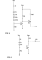
- a diode D3 may be used as the coupling gate as'illustrated in Figure 4. Components the same as or analogous to those of Figures 2 and 3 are designated by the same symbols.
- the circuit of Figure 4 provides introduction of an independent backup power supply V BB through the coupling gate D3 at. a desired threshold voltage level.
- the circuit may be used in applications where a subcircuit or circuit device is to be maintained in an active state despite power outage, for example, as a backup for active memories.
- FIG. 5 Another variation of the threshold activation circuit of the type illustrated in Figure 3 is shown in Figure 5.
- the coupling gate at the output of the threshold activation circuit is a field effect transistor FETand may be useful., for example, in applications with memory boards.
- the threshold activation circuit in accordance with the present invention is useful and applicable for sequencing the turn on or turn off of multiple -circuit devices, subcircuits or circuit portions dependent upon a common power supply.
- the invention is also applicable for introducing a backup power supply at the desired threshold voltage level of a conventional power supply, no.t only for sequencing multiple circuits, but-also for maintaining external circuits, circuit devices, subcircuits, etc. in an active state during power outage.
Landscapes
- Engineering & Computer Science (AREA)
- Power Engineering (AREA)
- Physics & Mathematics (AREA)
- Computer Hardware Design (AREA)
- Computing Systems (AREA)
- General Engineering & Computer Science (AREA)
- Mathematical Physics (AREA)
- Logic Circuits (AREA)
- Power Sources (AREA)
- Electronic Switches (AREA)
Applications Claiming Priority (2)
| Application Number | Priority Date | Filing Date | Title |
|---|---|---|---|
| US06/404,318 US4481430A (en) | 1982-08-02 | 1982-08-02 | Power supply threshold activation circuit |
| US404318 | 1982-08-02 |
Publications (3)
| Publication Number | Publication Date |
|---|---|
| EP0100737A2 true EP0100737A2 (de) | 1984-02-15 |
| EP0100737A3 EP0100737A3 (en) | 1985-01-16 |
| EP0100737B1 EP0100737B1 (de) | 1988-09-21 |
Family
ID=23599142
Family Applications (1)
| Application Number | Title | Priority Date | Filing Date |
|---|---|---|---|
| EP83401593A Expired EP0100737B1 (de) | 1982-08-02 | 1983-08-01 | Freigabegatter für drei Zustände mit Schwellschaltung zur Aktivierung der Speisespannung |
Country Status (5)
| Country | Link |
|---|---|
| US (1) | US4481430A (de) |
| EP (1) | EP0100737B1 (de) |
| JP (1) | JPS5949620A (de) |
| CA (1) | CA1201765A (de) |
| DE (1) | DE3378097D1 (de) |
Families Citing this family (18)
| Publication number | Priority date | Publication date | Assignee | Title |
|---|---|---|---|---|
| JPS5961046A (ja) * | 1982-09-30 | 1984-04-07 | Fujitsu Ltd | 集積回路装置 |
| US4661727A (en) * | 1984-07-19 | 1987-04-28 | Fairchild Semiconductor Corporation | Multiple phase-splitter TTL output circuit with improved drive characteristics |
| US4683383A (en) * | 1984-07-19 | 1987-07-28 | Tandem Computers Incorporated | Driver circuit for a three-state gate array using low driving current |
| US4839538A (en) * | 1986-12-16 | 1989-06-13 | Texas Instruments Incorporated | Impact bipolar integrated circuit designed to eliminate output glitches caused by negative chip ground spikes |
| KR900001746B1 (ko) * | 1987-01-24 | 1990-03-19 | 삼성반도체통신 주식회사 | 바이 씨 모스에 의한 고전압 대전력 구동회로 |
| US4890015A (en) * | 1988-01-29 | 1989-12-26 | Texas Instruments Incorporated | Method and circuitry for controlling the compensation of negative internal ground voltage fluctuations |
| US4871926A (en) * | 1988-09-06 | 1989-10-03 | Motorola, Inc. | Low power, three state power up circuit |
| FR2649270B1 (fr) * | 1989-06-30 | 1993-12-31 | Alcatel Cit | Dispositif de protection pour systeme de transmission de signaux numeriques |
| US5051611A (en) * | 1989-12-20 | 1991-09-24 | Quadic Systems, Inc. | Power-up circuit with hysteresis for an output buffer |
| US5051623A (en) * | 1990-06-16 | 1991-09-24 | National Semiconductor Corporation | TTL tristate circuit for output pulldown transistor |
| JPH084642Y2 (ja) * | 1991-04-26 | 1996-02-07 | 環境庁国立環境研究所長 | 車輌のヘッドライト構造 |
| US5373227A (en) * | 1993-03-26 | 1994-12-13 | Micron Semiconductor, Inc. | Control circuit responsive to its supply voltage level |
| US5565807A (en) * | 1994-09-16 | 1996-10-15 | National Semiconductor Corporation | BiCMOS power-up circuit with hysteresis |
| US5617048A (en) * | 1994-09-19 | 1997-04-01 | National Semiconductor Corporation | Hysteretic power-up circuit |
| DE19505269C1 (de) * | 1995-02-16 | 1996-05-23 | Siemens Ag | Integrierbare Schaltungsanordnung zur Arbeitsstromstabilisierung eines Transistors durch Gegenkopplung, insbesondere geeignet für batteriebetriebene Geräte |
| US6205500B1 (en) * | 1997-09-24 | 2001-03-20 | Compaq Computer Corp. | System and method for electrically isolating a device from higher voltage devices |
| EP1116327B1 (de) * | 1998-09-23 | 2003-10-01 | Robert Bosch Gmbh | Eingangsschaltung für eine endstufe |
| US7793178B2 (en) * | 2006-07-12 | 2010-09-07 | Texas Instruments Incorporated | Cell supporting scan-based tests and with reduced time delay in functional mode |
Family Cites Families (10)
| Publication number | Priority date | Publication date | Assignee | Title |
|---|---|---|---|---|
| US3725675A (en) * | 1971-03-29 | 1973-04-03 | Honeywell Inf Systems | Power sequencing control circuit |
| US4174541A (en) * | 1976-12-01 | 1979-11-13 | Raytheon Company | Bipolar monolithic integrated circuit memory with standby power enable |
| JPS5951177B2 (ja) * | 1977-03-12 | 1984-12-12 | 日本電気株式会社 | オ−トクリア信号発生回路 |
| JPS54945A (en) * | 1977-06-06 | 1979-01-06 | Nec Corp | Integrated circuit providing output control function |
| DE2733264C3 (de) * | 1977-07-22 | 1980-02-07 | Siemens Ag, 1000 Berlin Und 8000 Muenchen | Schaltungsanordnung zur Erzeugung eines Impulses zum Setzen der Elektronik eines elektronischen Gerätes, insbesondere eines elektronischen Maximumwerkes |
| JPS5493343A (en) * | 1977-12-30 | 1979-07-24 | Fujitsu Ltd | Semiconductor integrated circuit |
| US4260909A (en) * | 1978-08-30 | 1981-04-07 | Bell Telephone Laboratories, Incorporated | Back gate bias voltage generator circuit |
| US4288865A (en) * | 1980-02-06 | 1981-09-08 | Mostek Corporation | Low-power battery backup circuit for semiconductor memory |
| US4398106A (en) * | 1980-12-19 | 1983-08-09 | International Business Machines Corporation | On-chip Delta-I noise clamping circuit |
| US4415817A (en) * | 1981-10-08 | 1983-11-15 | Signetics Corporation | Bipolar logic gate including circuitry to prevent turn-off and deep saturation of pull-down transistor |
-
1982
- 1982-08-02 US US06/404,318 patent/US4481430A/en not_active Expired - Lifetime
-
1983
- 1983-07-29 CA CA000433643A patent/CA1201765A/en not_active Expired
- 1983-08-01 EP EP83401593A patent/EP0100737B1/de not_active Expired
- 1983-08-01 DE DE8383401593T patent/DE3378097D1/de not_active Expired
- 1983-08-02 JP JP58140627A patent/JPS5949620A/ja active Pending
Also Published As
| Publication number | Publication date |
|---|---|
| EP0100737A3 (en) | 1985-01-16 |
| US4481430A (en) | 1984-11-06 |
| DE3378097D1 (en) | 1988-10-27 |
| JPS5949620A (ja) | 1984-03-22 |
| CA1201765A (en) | 1986-03-11 |
| EP0100737B1 (de) | 1988-09-21 |
Similar Documents
| Publication | Publication Date | Title |
|---|---|---|
| US4481430A (en) | Power supply threshold activation circuit | |
| EP0780983B1 (de) | Spannungsregelumsetzer | |
| EP0267017B1 (de) | TTL/CMOS-kompatible Eingangspufferschaltung | |
| US5338978A (en) | Full swing power down buffer circuit with multiple power supply isolation | |
| US4800303A (en) | TTL compatible output buffer | |
| US6040729A (en) | Digital output buffer for multiple voltage system | |
| US4333020A (en) | MOS Latch circuit | |
| US5216297A (en) | Low voltage swing output mos circuit for driving an ecl circuit | |
| EP0367612B1 (de) | Lastgesteuerter ECL-Treiber | |
| EP0546724B1 (de) | BICMOS-Bus-Ausgangstreiber kompatibel mit einem Mischspannungssystem | |
| US6252423B1 (en) | Voltage tolerant interface circuit | |
| EP0621692A2 (de) | Überspannungsschutzschaltung | |
| EP0211553B1 (de) | Einschaltrücksetzschaltungsanordnungen | |
| US5298807A (en) | Buffer circuitry for transferring signals from TTL circuitry to dual range CMOS circuitry | |
| JPS61283092A (ja) | リセツトあるいはセツト付記憶回路を有した半導体集積回路 | |
| US4112314A (en) | Logical current switch | |
| EP0176255B1 (de) | Galliumarsenid-Logik mit phasenmodulierten Ausgangsimpulsen | |
| EP0463261A1 (de) | IC-Karte mit verbesserter Umschaltung der Stromversorgung | |
| US4791322A (en) | TTL compatible input buffer | |
| US3953746A (en) | Selector latch gate | |
| US5828233A (en) | Mixed mode CMOS input buffer with bus hold | |
| US4567575A (en) | Voltage level compensating interface circuit for inter-logic circuit data transmission system | |
| EP1057262A1 (de) | Gegen überspannungen geschützter eingangs/ausgangpuffer | |
| EP0450453B1 (de) | BICMOS-Eingangsschaltkreis zur Erkennung von Signalen ausserhalb des ECL-Bereiches | |
| CA1257355A (en) | Circuit arrangement for the transmission of binary signals |
Legal Events
| Date | Code | Title | Description |
|---|---|---|---|
| PUAI | Public reference made under article 153(3) epc to a published international application that has entered the european phase |
Free format text: ORIGINAL CODE: 0009012 |
|
| AK | Designated contracting states |
Designated state(s): DE FR GB IT NL |
|
| PUAL | Search report despatched |
Free format text: ORIGINAL CODE: 0009013 |
|
| AK | Designated contracting states |
Designated state(s): DE FR GB IT NL |
|
| 17P | Request for examination filed |
Effective date: 19850610 |
|
| 17Q | First examination report despatched |
Effective date: 19860212 |
|
| GRAA | (expected) grant |
Free format text: ORIGINAL CODE: 0009210 |
|
| RAP1 | Party data changed (applicant data changed or rights of an application transferred) |
Owner name: FAIRCHILD SEMICONDUCTOR CORPORATION |
|
| AK | Designated contracting states |
Kind code of ref document: B1 Designated state(s): DE FR GB IT NL |
|
| REF | Corresponds to: |
Ref document number: 3378097 Country of ref document: DE Date of ref document: 19881027 |
|
| ITF | It: translation for a ep patent filed | ||
| ET | Fr: translation filed | ||
| PLBE | No opposition filed within time limit |
Free format text: ORIGINAL CODE: 0009261 |
|
| STAA | Information on the status of an ep patent application or granted ep patent |
Free format text: STATUS: NO OPPOSITION FILED WITHIN TIME LIMIT |
|
| 26N | No opposition filed | ||
| ITTA | It: last paid annual fee | ||
| PGFP | Annual fee paid to national office [announced via postgrant information from national office to epo] |
Ref country code: GB Payment date: 19940711 Year of fee payment: 12 |
|
| PGFP | Annual fee paid to national office [announced via postgrant information from national office to epo] |
Ref country code: FR Payment date: 19940812 Year of fee payment: 12 |
|
| PGFP | Annual fee paid to national office [announced via postgrant information from national office to epo] |
Ref country code: NL Payment date: 19940831 Year of fee payment: 12 |
|
| PG25 | Lapsed in a contracting state [announced via postgrant information from national office to epo] |
Ref country code: GB Effective date: 19950801 |
|
| PG25 | Lapsed in a contracting state [announced via postgrant information from national office to epo] |
Ref country code: NL Effective date: 19960301 |
|
| GBPC | Gb: european patent ceased through non-payment of renewal fee |
Effective date: 19950801 |
|
| PG25 | Lapsed in a contracting state [announced via postgrant information from national office to epo] |
Ref country code: FR Effective date: 19960430 |
|
| NLV4 | Nl: lapsed or anulled due to non-payment of the annual fee |
Effective date: 19960301 |
|
| REG | Reference to a national code |
Ref country code: FR Ref legal event code: ST |
|
| PGFP | Annual fee paid to national office [announced via postgrant information from national office to epo] |
Ref country code: DE Payment date: 19960828 Year of fee payment: 14 |
|
| PG25 | Lapsed in a contracting state [announced via postgrant information from national office to epo] |
Ref country code: DE Free format text: LAPSE BECAUSE OF NON-PAYMENT OF DUE FEES Effective date: 19980501 |