EP0096625B1 - Structure de doigt d'émetteur dans un transistor de commutation et procédé de fabrication - Google Patents
Structure de doigt d'émetteur dans un transistor de commutation et procédé de fabrication Download PDFInfo
- Publication number
- EP0096625B1 EP0096625B1 EP83401076A EP83401076A EP0096625B1 EP 0096625 B1 EP0096625 B1 EP 0096625B1 EP 83401076 A EP83401076 A EP 83401076A EP 83401076 A EP83401076 A EP 83401076A EP 0096625 B1 EP0096625 B1 EP 0096625B1
- Authority
- EP
- European Patent Office
- Prior art keywords
- depth
- gold
- emitter
- zones
- central zone
- Prior art date
- Legal status (The legal status is an assumption and is not a legal conclusion. Google has not performed a legal analysis and makes no representation as to the accuracy of the status listed.)
- Expired
Links
- 238000004519 manufacturing process Methods 0.000 title description 7
- PCHJSUWPFVWCPO-UHFFFAOYSA-N gold Chemical group [Au] PCHJSUWPFVWCPO-UHFFFAOYSA-N 0.000 claims description 23
- 229910052737 gold Inorganic materials 0.000 claims description 21
- 239000010931 gold Substances 0.000 claims description 21
- 238000001465 metallisation Methods 0.000 claims description 17
- 229910052785 arsenic Inorganic materials 0.000 claims description 14
- RQNWIZPPADIBDY-UHFFFAOYSA-N arsenic atom Chemical group [As] RQNWIZPPADIBDY-UHFFFAOYSA-N 0.000 claims description 13
- 238000009792 diffusion process Methods 0.000 claims description 12
- OAICVXFJPJFONN-UHFFFAOYSA-N Phosphorus Chemical compound [P] OAICVXFJPJFONN-UHFFFAOYSA-N 0.000 claims description 11
- 229910052698 phosphorus Inorganic materials 0.000 claims description 11
- VYPSYNLAJGMNEJ-UHFFFAOYSA-N Silicium dioxide Chemical compound O=[Si]=O VYPSYNLAJGMNEJ-UHFFFAOYSA-N 0.000 claims description 10
- 239000011574 phosphorus Substances 0.000 claims description 10
- 230000005496 eutectics Effects 0.000 claims description 6
- 229910052710 silicon Inorganic materials 0.000 claims description 5
- 239000010703 silicon Substances 0.000 claims description 5
- 239000000377 silicon dioxide Substances 0.000 claims description 4
- 238000000151 deposition Methods 0.000 claims description 3
- 230000008021 deposition Effects 0.000 claims description 3
- 230000000873 masking effect Effects 0.000 claims description 3
- 238000000034 method Methods 0.000 claims description 2
- 239000000126 substance Substances 0.000 claims description 2
- 125000004429 atom Chemical group 0.000 description 7
- 238000002347 injection Methods 0.000 description 5
- 239000007924 injection Substances 0.000 description 5
- XUIMIQQOPSSXEZ-UHFFFAOYSA-N Silicon Chemical compound [Si] XUIMIQQOPSSXEZ-UHFFFAOYSA-N 0.000 description 4
- 239000002019 doping agent Substances 0.000 description 4
- 238000010438 heat treatment Methods 0.000 description 2
- 230000002411 adverse Effects 0.000 description 1
- XAGFODPZIPBFFR-UHFFFAOYSA-N aluminium Chemical compound [Al] XAGFODPZIPBFFR-UHFFFAOYSA-N 0.000 description 1
- 229910052782 aluminium Inorganic materials 0.000 description 1
- QZPSXPBJTPJTSZ-UHFFFAOYSA-N aqua regia Chemical compound Cl.O[N+]([O-])=O QZPSXPBJTPJTSZ-UHFFFAOYSA-N 0.000 description 1
- 230000004888 barrier function Effects 0.000 description 1
- 230000015572 biosynthetic process Effects 0.000 description 1
- 230000000903 blocking effect Effects 0.000 description 1
- 230000007547 defect Effects 0.000 description 1
- 238000002955 isolation Methods 0.000 description 1
- 239000004065 semiconductor Substances 0.000 description 1
- 229910052814 silicon oxide Inorganic materials 0.000 description 1
- 238000004544 sputter deposition Methods 0.000 description 1
- 230000007847 structural defect Effects 0.000 description 1
- 239000000758 substrate Substances 0.000 description 1
Images
Classifications
-
- H—ELECTRICITY
- H10—SEMICONDUCTOR DEVICES; ELECTRIC SOLID-STATE DEVICES NOT OTHERWISE PROVIDED FOR
- H10D—INORGANIC ELECTRIC SEMICONDUCTOR DEVICES
- H10D62/00—Semiconductor bodies, or regions thereof, of devices having potential barriers
- H10D62/10—Shapes, relative sizes or dispositions of the regions of the semiconductor bodies; Shapes of the semiconductor bodies
- H10D62/13—Semiconductor regions connected to electrodes carrying current to be rectified, amplified or switched, e.g. source or drain regions
- H10D62/133—Emitter regions of BJTs
- H10D62/136—Emitter regions of BJTs of heterojunction BJTs
-
- H—ELECTRICITY
- H10—SEMICONDUCTOR DEVICES; ELECTRIC SOLID-STATE DEVICES NOT OTHERWISE PROVIDED FOR
- H10D—INORGANIC ELECTRIC SEMICONDUCTOR DEVICES
- H10D62/00—Semiconductor bodies, or regions thereof, of devices having potential barriers
- H10D62/80—Semiconductor bodies, or regions thereof, of devices having potential barriers characterised by the materials
- H10D62/83—Semiconductor bodies, or regions thereof, of devices having potential barriers characterised by the materials being Group IV materials, e.g. B-doped Si or undoped Ge
- H10D62/834—Semiconductor bodies, or regions thereof, of devices having potential barriers characterised by the materials being Group IV materials, e.g. B-doped Si or undoped Ge further characterised by the dopants
Definitions
- the present invention relates to the field of transistors and, more particularly, medium and high power transistors used in switching, that is to say capable of passing very quickly from the conducting state to the blocked state.
- These transistors commonly have interdigitated emitter and base structures, that is to say that the emitter and base areas at least partially comprise portions in the form of overlapping bands.
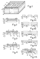
- FIG. 1 represents a partial view in section and in perspective of a digitized emitter transistor, this view being schematic.
- This transistor comprises collector layers 1 and 2, of type N + and N, and a base layer 3 of type P, in which are formed, generally by diffusion, emitter zones 4 of type N + having the form elongated fingers. Between the emitter fingers 4 there are possibly base fingers 5 made up of P-type zones with a doping level higher than the doping level of the layer 3 so as to promote the ohmicity of the contacts. Above the emitter diffusions 4, there are emitter metallizations 6 and, between these emitter metallizations, there are basic metallizations 7. The underside is coated with a collector metallization 8. The face upper part of the wafer, outside the areas of contact with the metallizations, is protected by a layer of silicon oxide 9 (Si02).
- Si02 silicon oxide 9
- Figure 2 shows an enlarged and schematic sectional view of the structure of a transmitter finger.
- the base layer 3 the emitter area 4, the emitter metallization 6 and the oxide layer 9.
- the lateral parts of the emitter zone which will be affected first by the currents coming from the adjacent base electrodes 7 and the current lines are concentrated in the central part of the emitter zone. This phenomenon of concentration of current lines at the opening which slows the switching to blocking of a transistor has been studied by many authors under the name of focusing of current lines.
- a first remedy illustrated in FIG. 3, consists quite simply in removing the central part of the emitter finger and covering it with an oxide layer 10 before proceeding to metallization 6.
- Each emitter finger is then divided in two separate fingers 11 and 12 connected by the metallization 6, this metallization having substantially the same width and the same thickness as that shown in FIG. 2, the section of this metallization being determined as a function of the current which it is desired to pass through the transmitter and to obtain a substantially equipotential surface over the entire surface of the transmitter area.
- a disadvantage of the structure of FIG. 3 is that if the oxide layer 10 has a defect (a hole), the metallization 6 will short-circuit the base and emitter zones.
- each emitter finger is also divided into two bands 11 and 12, but where a diffusion 13 of doping atoms of the same type as those of zones 11 and 12 is provided in the central part and where the metallization 6 rests on the entire emitter zone including on the central part without isolation (see for example GB-A-2 026 236).
- This avoids any base / emitter short circuits that may result from structural defects in the oxide layer 10 of FIG. 3.
- the structure of FIG. 4 has the obvious drawback of being less effective than the structure. in Figure 3 because there is still an injection at the central part 13 of the transmitter.
- the object of the first invention is to provide a new transmitter finger structure which avoids the aforementioned drawbacks of known structures and makes it possible to obtain higher switching switching speeds.
- the present invention relates more particularly to the case of NPN transistors and a method of manufacturing such transistors.
- FIGS. 5A to 5E illustrate specific steps for manufacturing a transmitter finger according to the present invention.
- two bands 11 and 12 of an emitting finger are formed by diffusion of phosphorus to obtain N + type emitter zones having a surface concentration of doping atoms greater than 10 20 atoms / cm 3 .
- a second step, illustrated in FIG. 5B the structure is masked by means of a layer of silica 20 and a layer of gold 21 comprising arsenic is deposited, for example by sputtering.
- heating is carried out in order to obtain a layer 22 of gold / silicon eutectic doped with arsenic.
- the gold layer 21 is then removed by an attack with aqua regia. Note that we could also have removed most of the gold layer outside the areas between bands 11 and 12 before proceeding to the eutectic formation step to avoid possible crossings by the gold from the silica layer 20. In this case, after the eutectic has been formed, the remaining portions of gold will be removed above the central bands located between bands 11 and 12.
- the eutectic layer 22 is again carried out to cause the gold and arsenic contained in the eutectic layer 22 to diffuse into the silicon, then the eutectic is removed by an attack Selective chemical. As is known, it gets faster than arsenic.
- This diffusion step is stopped when the gold has penetrated into the silicon substrate to a depth substantially equal to the junction depth of the emitter zones 11 and 12.
- the junction depth 23 of the arsenic is then l order of the fifth of that of zones 11 and 12.
- Zone 24 doped with gold is hatched in the figure.
- the surface concentration of arsenic can be of some 10 19 atoms / cm 3 and its junction depth of the order of 0.5 to 2 ⁇ m while the junction depth of layers 11 and 12 is of the order of 4 to 10 ⁇ m.
- zones 11 and 12 are heavily doped with phosphorus and where arsenic is used as a dopant in the central zone.
- These characteristics constitute an element of the present invention. Indeed, it is necessary to choose successive dopants compatible and selective with respect to gold: it is necessary that the gold diffuses faster than the dopant contained in the central zone and it is also necessary that the dopant of the lateral zones 11 and 12 constitutes a barrier for gold, which is the case with phosphorus (gold cannot diffuse through a silicon zone in which the phosphorus concentration is greater than approximately 10 20 atoms / cm 3 ).
- the width of the opening in the masking layer 20 (FIG. 5B) is not critical and even if this opening extends a little over the central surface portions of zones 11 and 12, there is no 'there will still be no diffusion of gold in these areas which would adversely affect the quality of the injection at the useful parts of the transmitter.
Landscapes
- Bipolar Transistors (AREA)
Applications Claiming Priority (2)
| Application Number | Priority Date | Filing Date | Title |
|---|---|---|---|
| FR8209954 | 1982-06-08 | ||
| FR8209954A FR2528233A1 (fr) | 1982-06-08 | 1982-06-08 | Structure de doigt d'emetteur dans un transistor de commutation |
Publications (2)
| Publication Number | Publication Date |
|---|---|
| EP0096625A1 EP0096625A1 (fr) | 1983-12-21 |
| EP0096625B1 true EP0096625B1 (fr) | 1986-07-16 |
Family
ID=9274750
Family Applications (1)
| Application Number | Title | Priority Date | Filing Date |
|---|---|---|---|
| EP83401076A Expired EP0096625B1 (fr) | 1982-06-08 | 1983-05-27 | Structure de doigt d'émetteur dans un transistor de commutation et procédé de fabrication |
Country Status (4)
| Country | Link |
|---|---|
| US (1) | US4609414A (enExample) |
| EP (1) | EP0096625B1 (enExample) |
| DE (1) | DE3364513D1 (enExample) |
| FR (1) | FR2528233A1 (enExample) |
Families Citing this family (4)
| Publication number | Priority date | Publication date | Assignee | Title |
|---|---|---|---|---|
| GB2171555A (en) * | 1985-02-20 | 1986-08-28 | Philips Electronic Associated | Bipolar semiconductor device with implanted recombination region |
| JP2775503B2 (ja) * | 1990-03-13 | 1998-07-16 | 三菱電機株式会社 | 接合ゲート型電界効果トランジスタの製造方法 |
| JP5061407B2 (ja) * | 2001-01-31 | 2012-10-31 | 富士電機株式会社 | 半導体装置およびその製造方法 |
| US10199529B2 (en) * | 2008-05-28 | 2019-02-05 | Solar-Tectic, Llc | Methods of growing heteroepitaxial single crystal or large grained semiconductor films and devices thereon |
Citations (2)
| Publication number | Priority date | Publication date | Assignee | Title |
|---|---|---|---|---|
| EP0011120A1 (fr) * | 1978-11-09 | 1980-05-28 | International Business Machines Corporation | Dispositif semi-conducteur à gain de courant amélioré et son procédé de fabrication |
| EP0015835A2 (fr) * | 1979-03-09 | 1980-09-17 | Thomson-Csf | Dispositif semiconducteur de commutation à fréquence élevée et procédé pour sa fabrication |
Family Cites Families (9)
| Publication number | Priority date | Publication date | Assignee | Title |
|---|---|---|---|---|
| US3258371A (en) * | 1962-02-01 | 1966-06-28 | Semiconductor Res Found | Silicon semiconductor device for high frequency, and method of its manufacture |
| US3728592A (en) * | 1969-05-09 | 1973-04-17 | Ibm | Semiconductor structure having reduced carrier lifetime |
| US3943549A (en) * | 1972-03-15 | 1976-03-09 | Bbc Brown, Boveri & Company, Limited | Thyristor |
| JPS5342234B2 (enExample) * | 1973-02-12 | 1978-11-09 | ||
| US4177477A (en) * | 1974-03-11 | 1979-12-04 | Mitsubishi Denki Kabushiki Kaisha | Semiconductor switching device |
| FR2374743A1 (fr) * | 1976-12-20 | 1978-07-13 | Radiotechnique Compelec | Transistor multicouche a emetteur compose |
| FR2374742A1 (fr) * | 1976-12-20 | 1978-07-13 | Radiotechnique Compelec | Transistor multicouche pour tensions elevees et son procede de fabrication |
| GB2026236B (en) * | 1978-07-20 | 1983-02-02 | Gen Electric | Power transistor |
| US4345266A (en) * | 1978-07-20 | 1982-08-17 | General Electric Company | Transistor having improved turn-off time and second breakdown characteristics with bi-level emitter structure |
-
1982
- 1982-06-08 FR FR8209954A patent/FR2528233A1/fr active Granted
-
1983
- 1983-05-27 DE DE8383401076T patent/DE3364513D1/de not_active Expired
- 1983-05-27 EP EP83401076A patent/EP0096625B1/fr not_active Expired
- 1983-06-06 US US06/501,189 patent/US4609414A/en not_active Expired - Lifetime
Patent Citations (2)
| Publication number | Priority date | Publication date | Assignee | Title |
|---|---|---|---|---|
| EP0011120A1 (fr) * | 1978-11-09 | 1980-05-28 | International Business Machines Corporation | Dispositif semi-conducteur à gain de courant amélioré et son procédé de fabrication |
| EP0015835A2 (fr) * | 1979-03-09 | 1980-09-17 | Thomson-Csf | Dispositif semiconducteur de commutation à fréquence élevée et procédé pour sa fabrication |
Also Published As
| Publication number | Publication date |
|---|---|
| DE3364513D1 (en) | 1986-08-21 |
| EP0096625A1 (fr) | 1983-12-21 |
| FR2528233A1 (fr) | 1983-12-09 |
| FR2528233B1 (enExample) | 1985-05-17 |
| US4609414A (en) | 1986-09-02 |
Similar Documents
| Publication | Publication Date | Title |
|---|---|---|
| EP0881690B1 (fr) | Procédé de réalisation d'un transistor bipolaire stabilisé avec éléments isolants électriques | |
| EP0022388B1 (fr) | Procédé de fabrication d'un transistor à effet de champ du type DMOS à fonctionnement vertical | |
| EP1406307A1 (fr) | Circuit intégré à couche enterrée fortement conductrice | |
| EP0096625B1 (fr) | Structure de doigt d'émetteur dans un transistor de commutation et procédé de fabrication | |
| EP0069606B1 (fr) | Transistor à effet de champ vertical à jonction et procédé de fabrication | |
| EP0990266B1 (fr) | Transistor hyperfrequence a structure quasi-autoalignee et son procede de fabrication | |
| EP1132955A1 (fr) | Procédé de fabrication d'un transistor bipolaire double-polysilicium autoaligné. | |
| EP0414618B1 (fr) | Transistor MOS en couche mince avec la zone de canal reliée à la source et son procédé de fabrication | |
| EP0410911B1 (fr) | Procédé de fabrication d'un circuit intégré à transistors de puissance et logiques comprenant une diode. | |
| EP0002087A1 (fr) | Dispositif semiconducteur monolithique comprenant deux transistors complémentaires et son procédé de fabrication | |
| EP1058302A1 (fr) | Procédé de fabrication de dispositifs bipolaires à jonction base-émetteur autoalignée | |
| EP0197838B1 (fr) | Procédé de réalisation d'un transistor à effet de champ à métallisation de grille autoalignée | |
| EP1006573A1 (fr) | Procédé de fabrication de circuits intégrés BICMOS sur un substrat CMOS classique | |
| EP0164292B1 (fr) | Thyristor blocable à gachette d'anode | |
| EP0230840B1 (fr) | Transistor à base perméable et procédés de fabrication | |
| FR2864345A1 (fr) | Realisation de la peripherie d'une diode schottky a tranchees mos | |
| FR2530383A1 (fr) | Circuit integre monolithique comprenant une partie logique schottky et une memoire programmable a fusibles | |
| EP0949666A1 (fr) | Région de base-émetteur d'un transistor bipolaire submicronique | |
| EP0098209B1 (fr) | Transistor de commutation de puissance à structure digitée | |
| EP0037764B1 (fr) | Structure de dispositif à semiconducteur à anneau de garde, et à fonctionnement unipolaire | |
| EP0843349A1 (fr) | Procédé de fabrication d'un transistor NPN de surface minimale | |
| FR2963983A1 (fr) | Composant de protection bidirectionnel dissymetrique | |
| FR2557367A1 (fr) | Structure semiconductrice a tenue en tension elevee avec sillon peripherique implante et son procede de fabrication | |
| FR2760130A1 (fr) | Transistor mos a faible resistance de drain | |
| FR2528232A1 (fr) | Structure de contact sur une zone semi-conductrice superficielle fortement dopee et procede de fabrication |
Legal Events
| Date | Code | Title | Description |
|---|---|---|---|
| PUAI | Public reference made under article 153(3) epc to a published international application that has entered the european phase |
Free format text: ORIGINAL CODE: 0009012 |
|
| AK | Designated contracting states |
Designated state(s): DE FR GB IT |
|
| 17P | Request for examination filed |
Effective date: 19831229 |
|
| GRAA | (expected) grant |
Free format text: ORIGINAL CODE: 0009210 |
|
| AK | Designated contracting states |
Kind code of ref document: B1 Designated state(s): DE FR GB IT |
|
| ITF | It: translation for a ep patent filed | ||
| REF | Corresponds to: |
Ref document number: 3364513 Country of ref document: DE Date of ref document: 19860821 |
|
| PLBE | No opposition filed within time limit |
Free format text: ORIGINAL CODE: 0009261 |
|
| STAA | Information on the status of an ep patent application or granted ep patent |
Free format text: STATUS: NO OPPOSITION FILED WITHIN TIME LIMIT |
|
| 26N | No opposition filed | ||
| PG25 | Lapsed in a contracting state [announced via postgrant information from national office to epo] |
Ref country code: FR Free format text: LAPSE BECAUSE OF NON-PAYMENT OF DUE FEES Effective date: 19890131 |
|
| REG | Reference to a national code |
Ref country code: FR Ref legal event code: ST |
|
| ITTA | It: last paid annual fee | ||
| PGFP | Annual fee paid to national office [announced via postgrant information from national office to epo] |
Ref country code: DE Payment date: 20000522 Year of fee payment: 18 |
|
| PGFP | Annual fee paid to national office [announced via postgrant information from national office to epo] |
Ref country code: GB Payment date: 20000524 Year of fee payment: 18 |
|
| PG25 | Lapsed in a contracting state [announced via postgrant information from national office to epo] |
Ref country code: GB Free format text: LAPSE BECAUSE OF NON-PAYMENT OF DUE FEES Effective date: 20010527 |
|
| GBPC | Gb: european patent ceased through non-payment of renewal fee |
Effective date: 20010527 |
|
| PG25 | Lapsed in a contracting state [announced via postgrant information from national office to epo] |
Ref country code: DE Free format text: LAPSE BECAUSE OF NON-PAYMENT OF DUE FEES Effective date: 20020301 |