EP0094485A1 - Amplificateur différentiel à polarisation auto-adaptive - Google Patents
Amplificateur différentiel à polarisation auto-adaptive Download PDFInfo
- Publication number
- EP0094485A1 EP0094485A1 EP83102544A EP83102544A EP0094485A1 EP 0094485 A1 EP0094485 A1 EP 0094485A1 EP 83102544 A EP83102544 A EP 83102544A EP 83102544 A EP83102544 A EP 83102544A EP 0094485 A1 EP0094485 A1 EP 0094485A1
- Authority
- EP
- European Patent Office
- Prior art keywords
- differential amplifier
- voltage
- amplifier circuit
- amplifier
- circuit according
- Prior art date
- Legal status (The legal status is an assumption and is not a legal conclusion. Google has not performed a legal analysis and makes no representation as to the accuracy of the status listed.)
- Granted
Links
- 230000000087 stabilizing effect Effects 0.000 claims description 2
- 229920006395 saturated elastomer Polymers 0.000 description 3
- 230000003247 decreasing effect Effects 0.000 description 2
- 230000001934 delay Effects 0.000 description 2
- 230000001105 regulatory effect Effects 0.000 description 2
- 238000009738 saturating Methods 0.000 description 2
- 238000013459 approach Methods 0.000 description 1
- 239000003990 capacitor Substances 0.000 description 1
- 238000010586 diagram Methods 0.000 description 1
- 230000000694 effects Effects 0.000 description 1
- 230000007774 longterm Effects 0.000 description 1
- 238000004806 packaging method and process Methods 0.000 description 1
Images
Classifications
-
- H—ELECTRICITY
- H03—ELECTRONIC CIRCUITRY
- H03F—AMPLIFIERS
- H03F3/00—Amplifiers with only discharge tubes or only semiconductor devices as amplifying elements
- H03F3/45—Differential amplifiers
- H03F3/45071—Differential amplifiers with semiconductor devices only
- H03F3/45076—Differential amplifiers with semiconductor devices only characterised by the way of implementation of the active amplifying circuit in the differential amplifier
- H03F3/4508—Differential amplifiers with semiconductor devices only characterised by the way of implementation of the active amplifying circuit in the differential amplifier using bipolar transistors as the active amplifying circuit
- H03F3/45085—Long tailed pairs
-
- H—ELECTRICITY
- H03—ELECTRONIC CIRCUITRY
- H03F—AMPLIFIERS
- H03F1/00—Details of amplifiers with only discharge tubes, only semiconductor devices or only unspecified devices as amplifying elements
- H03F1/02—Modifications of amplifiers to raise the efficiency, e.g. gliding Class A stages, use of an auxiliary oscillation
- H03F1/0205—Modifications of amplifiers to raise the efficiency, e.g. gliding Class A stages, use of an auxiliary oscillation in transistor amplifiers
- H03F1/0261—Modifications of amplifiers to raise the efficiency, e.g. gliding Class A stages, use of an auxiliary oscillation in transistor amplifiers with control of the polarisation voltage or current, e.g. gliding Class A
-
- H—ELECTRICITY
- H03—ELECTRONIC CIRCUITRY
- H03F—AMPLIFIERS
- H03F2203/00—Indexing scheme relating to amplifiers with only discharge tubes or only semiconductor devices as amplifying elements covered by H03F3/00
- H03F2203/45—Indexing scheme relating to differential amplifiers
- H03F2203/45454—Indexing scheme relating to differential amplifiers the CSC comprising biasing means controlled by the input signal
-
- H—ELECTRICITY
- H03—ELECTRONIC CIRCUITRY
- H03F—AMPLIFIERS
- H03F2203/00—Indexing scheme relating to amplifiers with only discharge tubes or only semiconductor devices as amplifying elements covered by H03F3/00
- H03F2203/45—Indexing scheme relating to differential amplifiers
- H03F2203/45702—Indexing scheme relating to differential amplifiers the LC comprising two resistors
Definitions
- This invention relates to differential amplifier circuits in general, and more particularly to a differential amplifier circuit including means to bias the output transistors thereof to provide optimum speed, maximum voltage swing, and minimum power dissipation.
- a form of biasing that has heretofore been employed to control the current flow through the output devices of a differential amplifier is a variable current source connected between the junction of the two output devices and a voltage source.
- this current source is interposed between the junction of the emitters of these transistors and a negative voltage supply.
- Each of the prior art references shows an arrangement of a variable current source connected between the junction of the emitters of the differential amplifier output transistors (NPN) and a negative voltage supply although in none of these references is the current source varied in accordance with this invention to set a constant optimum current.
- NPN differential amplifier output transistors
- Patent US-A-3,435,365 a portion of the output current is used to control the variable current source interposed between the emitters of the output transistors and a negative voltage source. As the output signal increases this current feedback causes a decrease in the current through the amplifiers so that an automatic gain function is realized.
- Patent US-A-3,551,836 is similar to Patent US-A-3,435,365 in that the total amplifier output current is sampled and is used in a feedback path to vary the amplifier gain.
- the IBM Technical Disclosure Bulletin article of H.L. Funk describes another automatic gain control function implemented by using a variable current source between a junction of the emitters in an NPN differential amplifier and a negative voltage source.
- the amplifier output voltage is rectified and integrated to control the variable current source.
- the output voltage at each of the differential amplifier output transistor sampled and compared to a reference voltage or a base bias voltage of these transistors to maintain an optimum current flow through the amplifier to optimize the performance of the output transistors, keeping them out of saturation while otherwise maintaining a substantially low power dissipation.
- both of the amplifier outputs are sensed for the minimum voltage at either of these outputs.
- the lower of these voltages is compared with a reference voltage and circuitry is provided to maintain an optimum current flow through the amplifier which approaches a saturating current, but never saturates the output transistors.
- the differential amplifier provides maximum voltage swing and optimum speed with minimum power dissipation.
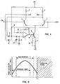
- transistors 1 and 2 are the output transistors of a differential amplifier circuit.
- the differential amplifier circuit of this figure is shown in a classical form. More complex differential amplifier circuits have been shown in the prior art to which this invention is equally applicable, including a differential amplifier in which each of the two legs comprises a cascode circuit arrangement instead of a single output transistor. For the purposes of this description, therefore, transistors 1 and 2 are considered the output transistors of any differential amplifier arrangement.
- FIG 2 a plot is shown of power dissipation in output transistors 1 and 2 versus collector current flow I through the transistors.
- the curve shown in figure 2 is representative of the power dissipation in the one of the two output transistors 1 and. 2 in which the greater collector current flows since, depending on the magnitude of the input voltage Vin relative to the reference voltage Vref, one of output transistors 1 and 2 is to be operated near saturation while the other of these two output transistors is to be operated at near cut-off.
- an input voltage Vin is applied to the base of output transistor 1 while a reference voltage Vref is applied to the base of output transistor 2.
- the collectors of these output transistors 1 and 2 are connected to a voltage source Vl through load resistors 3 and 4.
- transistors 1 and 2 are NPN and, therefore, the voltage source ends of resistors 3 and 4 are connected to the positive terminal of the voltage source, although, it will be obvious to those skilled in the art that PNP transistors could be used throughout the circuit of figure 1, rather than NPN transistors with opposite polarities of the two voltage sources.
- the output voltages V01 and V02 are taken at the collectors of the output transistors 1 and 2.
- the emitters of transistors 1 and 2 are connected together and are also connected to the collector of transistor 5 which forms the output portion of the automatically adjusted current source of the differential amplifier.
- the emitter of transistor 5 is connected through a resistor 6 to a negative potential V2 while the base of transistor 5 is connected through resistor 15 to the output of operational amplifier 7, the operation of which, in conjunction with the remainder of the automatic biasing circuitry, will now be described in detail.
- the cathodes of diodes 8 and 9 are connected to the collectors of output transistors 1 and 2, respectively.
- the anode of diodes 8 and 9 are connected together at the non-inverting input of operational amplifier 7.
- Resistors 10 and 11 form a DC voltage divider with the ratio of the resistors chosen to initially provide, during circuit starting, a voltage at the non-inverting input of amplifier 7 which is slightly greater than one diode drop more than the lower of the two V01, V02 output voltages.
- Vref is set at 2.0 volts and that Vin has two states, the lower of wich is 1.5 volts and the upper of which is 2.5 volts.
- the ratio of resistors 12 and 13 and resistors 15 and 16 are chosen to control transistor 5 to draw current out of the emitters of transistors 1 and 2 as required to maintain V01 and V 02 at the chosen output magnitudes, which will insure that neither of these transistors is driven to the point of saturation.
- the collector of transistor 5 is at 1.8 volts and the emitter voltage of transistor 5 is determined by the current through the differential amplifier circuit (approximately 27 volts divided by the resistance of resistor 4 multiplied by the resistance of resistor 6 algebraically added to the potential of the negative voltage V2).
- the base voltage of transistor 5 is then assumed to be 0.7 volts higher than the emitter voltage of transistor 5 and, therefore, the ratio of the resistance of resistors 15 and 16 can be determined.
- the ratio of resistors 12 and 13 and the ratio of resistors 15 and 16 determine the amount of current flow through the higher current leg of the differential amplifier circuit which, in turn, sets the voltages V01 and V02.
- V01 will cause V01 to rise which would increase the voltage at the inputs of amplifier 7.
- This will result in more current being drawn through resistors 12 and 13 and, therefore, a higher positive voltage at the output of amplifier 7.
- This provides a less negative voltage at the base of transistor 5 and, therefore, a greater current flow through transistor 5 and out of the differential amplifier.
- This greater current flow out of the differential amplifier provides a greater voltage drop across resistor 3 which lcwers the output voltage V01 back down to the 3 volt level.
- a decrease in Vl causes a lower current to flow to maintain the same V01.
- transistor 1 When the Vin voltage was dropped below the Vref voltage, transistor 1 was turned off. During any switchover capacitor 17 serves to momentarily hold the voltage at the inputs of amplifier 7 at the level immediately prior to the switchover for stabilizing purposes. It is also assumed that amplifier 7 has relatively slow response or some equivalent capacitance between the inverting input and the output.
- an improved differential amplifier circuit which includes an automatic bias adjustment circuit in which the amplifier outputs are sensed for the minimum voltage at either of these outputs. The lower of these voltages is compared with a base bias voltage which, in the case of the amplifier shown, is the reference voltage applied as one of the differential amplifier inputs. Circuitry is provided to maintain an optimum current flow through the amplifier to provide a maximum voltage swing and optimum speed of the amplifier by not saturating the output transistors while also providing a minimum power dissipation by regulating this current at a level approaching saturation.
- each of the two output stages of the differential amplifier while shown in the simpliest form for this description, might, instead be comprised of cascode circuitry.
Landscapes
- Engineering & Computer Science (AREA)
- Power Engineering (AREA)
- Amplifiers (AREA)
Applications Claiming Priority (2)
| Application Number | Priority Date | Filing Date | Title |
|---|---|---|---|
| US377771 | 1982-05-13 | ||
| US06/377,771 US4442408A (en) | 1982-05-13 | 1982-05-13 | Differential amplifier with auto bias adjust |
Publications (2)
| Publication Number | Publication Date |
|---|---|
| EP0094485A1 true EP0094485A1 (fr) | 1983-11-23 |
| EP0094485B1 EP0094485B1 (fr) | 1986-07-02 |
Family
ID=23490467
Family Applications (1)
| Application Number | Title | Priority Date | Filing Date |
|---|---|---|---|
| EP83102544A Expired EP0094485B1 (fr) | 1982-05-13 | 1983-03-15 | Amplificateur différentiel à polarisation auto-adaptive |
Country Status (5)
| Country | Link |
|---|---|
| US (1) | US4442408A (fr) |
| EP (1) | EP0094485B1 (fr) |
| JP (1) | JPS58206211A (fr) |
| CA (1) | CA1187144A (fr) |
| DE (1) | DE3364320D1 (fr) |
Cited By (4)
| Publication number | Priority date | Publication date | Assignee | Title |
|---|---|---|---|---|
| EP0173370A1 (fr) * | 1984-08-20 | 1986-03-05 | Koninklijke Philips Electronics N.V. | Montage amplificateur |
| DE3522416A1 (de) * | 1985-06-22 | 1987-01-02 | Standard Elektrik Lorenz Ag | Regelbare breitbandverstaerkerschaltung |
| DE3614691A1 (de) * | 1986-04-30 | 1987-11-05 | Siemens Ag | Integrierbarer impulsverstaerker |
| EP0468760A1 (fr) * | 1990-07-27 | 1992-01-29 | Motorola, Inc. | Amplificateur à deux modes d'opération |
Families Citing this family (13)
| Publication number | Priority date | Publication date | Assignee | Title |
|---|---|---|---|---|
| IT1185638B (it) * | 1985-07-18 | 1987-11-12 | Sgs Microelettronica Spa | Amplificatore operazionale tutto differenziale per circuiti integrati in tecnologia mos |
| US4951002A (en) * | 1989-04-13 | 1990-08-21 | Plantronics, Inc. | Battery powered in-line amplifier |
| US5115206A (en) * | 1990-11-08 | 1992-05-19 | North American Philips Corp., Signetics Division | Merged differential amplifier and current source |
| US5589796A (en) * | 1994-11-01 | 1996-12-31 | Motorola, Inc | Method and apparatus for increasing amplifier efficiency |
| US5572166A (en) * | 1995-06-07 | 1996-11-05 | Analog Devices, Inc. | Linear-in-decibel variable gain amplifier |
| US5821809A (en) * | 1996-05-23 | 1998-10-13 | International Business Machines Corporation | CMOS high-speed differential to single-ended converter circuit |
| EP0919082B1 (fr) * | 1997-06-25 | 2004-01-21 | Koninklijke Philips Electronics N.V. | Amplificateur differentiel, circuit integre et telephone |
| DE19841718C2 (de) | 1998-09-11 | 2001-01-25 | St Microelectronics Gmbh | Komparator |
| US6218902B1 (en) * | 1999-04-20 | 2001-04-17 | Nortel Networks Limited | Wide-band linearization technique |
| DE10341320B4 (de) * | 2003-09-08 | 2007-05-10 | Infineon Technologies Ag | Differenzverstärkerschaltung |
| DE102004024082A1 (de) * | 2004-05-14 | 2005-12-08 | Infineon Technologies Ag | Eingangsschaltung zum Empfangen eines Eingangssignals sowie ein Verfahren zum Anpassen eines Arbeitspunktes einer Eingangsschaltung |
| JP4578896B2 (ja) * | 2004-08-26 | 2010-11-10 | ルネサスエレクトロニクス株式会社 | クロックバッファ回路 |
| US7554402B2 (en) * | 2007-11-01 | 2009-06-30 | Analog Devices, Inc. | High CMR amplifier topology |
Citations (5)
| Publication number | Priority date | Publication date | Assignee | Title |
|---|---|---|---|---|
| US3435365A (en) * | 1965-10-01 | 1969-03-25 | Ibm | Monolithically fabricated operational amplifier device with self-drive |
| US3733559A (en) * | 1970-06-29 | 1973-05-15 | Rca Corp | Differential amplifier |
| DE1901804B2 (de) * | 1965-12-13 | 1976-02-05 | International Business Machines Corp., Armonk, N.Y. (V.St.A.) | Stabilisierter differentialverstaerker |
| DE2631916B2 (de) * | 1975-07-15 | 1980-08-28 | Commissariat A L'energie Atomique, Paris | Auf einem Halbleiterchip aufgebauter Differenzverstärker mit MOS-Feldeffekttransistoren |
| DE2758933B2 (de) * | 1976-12-31 | 1980-09-04 | Thomson-Csf, Paris | Linearer Transistor-Leistungsverstärker |
Family Cites Families (3)
| Publication number | Priority date | Publication date | Assignee | Title |
|---|---|---|---|---|
| US3434069A (en) * | 1967-04-27 | 1969-03-18 | North American Rockwell | Differential amplifier having a feedback path including a differential current generator |
| US3721914A (en) * | 1970-03-27 | 1973-03-20 | Sansui Electric Co | Differential amplifier having balanced current flow |
| SE416694B (sv) * | 1979-03-09 | 1981-01-26 | Ericsson Telefon Ab L M | Forsterkningsregleringskoppling |
-
1982
- 1982-05-13 US US06/377,771 patent/US4442408A/en not_active Expired - Lifetime
-
1983
- 1983-03-15 DE DE8383102544T patent/DE3364320D1/de not_active Expired
- 1983-03-15 EP EP83102544A patent/EP0094485B1/fr not_active Expired
- 1983-03-16 JP JP58042498A patent/JPS58206211A/ja active Granted
- 1983-05-02 CA CA000427173A patent/CA1187144A/fr not_active Expired
Patent Citations (5)
| Publication number | Priority date | Publication date | Assignee | Title |
|---|---|---|---|---|
| US3435365A (en) * | 1965-10-01 | 1969-03-25 | Ibm | Monolithically fabricated operational amplifier device with self-drive |
| DE1901804B2 (de) * | 1965-12-13 | 1976-02-05 | International Business Machines Corp., Armonk, N.Y. (V.St.A.) | Stabilisierter differentialverstaerker |
| US3733559A (en) * | 1970-06-29 | 1973-05-15 | Rca Corp | Differential amplifier |
| DE2631916B2 (de) * | 1975-07-15 | 1980-08-28 | Commissariat A L'energie Atomique, Paris | Auf einem Halbleiterchip aufgebauter Differenzverstärker mit MOS-Feldeffekttransistoren |
| DE2758933B2 (de) * | 1976-12-31 | 1980-09-04 | Thomson-Csf, Paris | Linearer Transistor-Leistungsverstärker |
Cited By (4)
| Publication number | Priority date | Publication date | Assignee | Title |
|---|---|---|---|---|
| EP0173370A1 (fr) * | 1984-08-20 | 1986-03-05 | Koninklijke Philips Electronics N.V. | Montage amplificateur |
| DE3522416A1 (de) * | 1985-06-22 | 1987-01-02 | Standard Elektrik Lorenz Ag | Regelbare breitbandverstaerkerschaltung |
| DE3614691A1 (de) * | 1986-04-30 | 1987-11-05 | Siemens Ag | Integrierbarer impulsverstaerker |
| EP0468760A1 (fr) * | 1990-07-27 | 1992-01-29 | Motorola, Inc. | Amplificateur à deux modes d'opération |
Also Published As
| Publication number | Publication date |
|---|---|
| JPH0147048B2 (fr) | 1989-10-12 |
| DE3364320D1 (en) | 1986-08-07 |
| EP0094485B1 (fr) | 1986-07-02 |
| CA1187144A (fr) | 1985-05-14 |
| US4442408A (en) | 1984-04-10 |
| JPS58206211A (ja) | 1983-12-01 |
Similar Documents
| Publication | Publication Date | Title |
|---|---|---|
| EP0094485B1 (fr) | Amplificateur différentiel à polarisation auto-adaptive | |
| EP0715238B1 (fr) | Circuit et méthode pour la régulation d'une tension | |
| US6559717B1 (en) | Method and/or architecture for implementing a variable gain amplifier control | |
| KR970004617B1 (ko) | 이득 제어 증폭 회로 | |
| KR20010020410A (ko) | 선형성 및 대역폭이 개선된 가변 이득 증폭기 | |
| KR101238173B1 (ko) | 고 슬루율과 고 단위 이득 대역폭을 가지는 저 드롭아웃 레귤레이터 | |
| JP3315748B2 (ja) | 増幅回路 | |
| KR900013705A (ko) | 회로 입력 신호의 차동 증폭용 전자회로 | |
| US3940708A (en) | Gain control circuit | |
| JP2590378B2 (ja) | 論理回路 | |
| US4709163A (en) | Current-discrimination arrangement | |
| US5262713A (en) | Current mirror for sensing current | |
| US4095126A (en) | Bi-polar amplifier with sharply defined amplitude limits | |
| US6292057B1 (en) | Output stage of an operational amplifier and method having a latchup-free sourcing current booster for driving low impedance loads | |
| CN114138043B (zh) | 线性稳压电路及电子设备 | |
| JP3273813B2 (ja) | 増幅器 | |
| US6741133B2 (en) | High output amplifier for stable operation | |
| US3448372A (en) | Apparatus for reducing the switching time of a dual voltage power supply | |
| US3651420A (en) | Variable gain direct coupled amplifier | |
| US5939907A (en) | Low power, high speed driving circuit for driving switching elements | |
| US6559706B2 (en) | Mixer circuitry | |
| US3952259A (en) | Gain control apparatus | |
| US4476444A (en) | Power amplifier circuit | |
| JPS6246328Y2 (fr) | ||
| KR940003612Y1 (ko) | 오디오증폭기의 출력전압 안정화회로 |
Legal Events
| Date | Code | Title | Description |
|---|---|---|---|
| PUAI | Public reference made under article 153(3) epc to a published international application that has entered the european phase |
Free format text: ORIGINAL CODE: 0009012 |
|
| AK | Designated contracting states |
Designated state(s): CH DE FR GB IT LI NL SE |
|
| 17P | Request for examination filed |
Effective date: 19840320 |
|
| GRAA | (expected) grant |
Free format text: ORIGINAL CODE: 0009210 |
|
| AK | Designated contracting states |
Kind code of ref document: B1 Designated state(s): CH DE FR GB IT LI NL SE |
|
| PG25 | Lapsed in a contracting state [announced via postgrant information from national office to epo] |
Ref country code: NL Effective date: 19860702 |
|
| REF | Corresponds to: |
Ref document number: 3364320 Country of ref document: DE Date of ref document: 19860807 |
|
| ET | Fr: translation filed | ||
| ITF | It: translation for a ep patent filed | ||
| NLV1 | Nl: lapsed or annulled due to failure to fulfill the requirements of art. 29p and 29m of the patents act | ||
| PLBE | No opposition filed within time limit |
Free format text: ORIGINAL CODE: 0009261 |
|
| STAA | Information on the status of an ep patent application or granted ep patent |
Free format text: STATUS: NO OPPOSITION FILED WITHIN TIME LIMIT |
|
| 26N | No opposition filed | ||
| ITTA | It: last paid annual fee | ||
| PGFP | Annual fee paid to national office [announced via postgrant information from national office to epo] |
Ref country code: CH Payment date: 19910625 Year of fee payment: 9 |
|
| PGFP | Annual fee paid to national office [announced via postgrant information from national office to epo] |
Ref country code: SE Payment date: 19920224 Year of fee payment: 10 |
|
| PG25 | Lapsed in a contracting state [announced via postgrant information from national office to epo] |
Ref country code: LI Effective date: 19920331 Ref country code: CH Effective date: 19920331 |
|
| REG | Reference to a national code |
Ref country code: CH Ref legal event code: PL |
|
| PGFP | Annual fee paid to national office [announced via postgrant information from national office to epo] |
Ref country code: GB Payment date: 19930216 Year of fee payment: 11 |
|
| PG25 | Lapsed in a contracting state [announced via postgrant information from national office to epo] |
Ref country code: SE Effective date: 19930316 |
|
| PGFP | Annual fee paid to national office [announced via postgrant information from national office to epo] |
Ref country code: DE Payment date: 19930406 Year of fee payment: 11 |
|
| PGFP | Annual fee paid to national office [announced via postgrant information from national office to epo] |
Ref country code: FR Payment date: 19940225 Year of fee payment: 12 |
|
| PG25 | Lapsed in a contracting state [announced via postgrant information from national office to epo] |
Ref country code: GB Effective date: 19940315 |
|
| GBPC | Gb: european patent ceased through non-payment of renewal fee |
Effective date: 19940315 |
|
| PG25 | Lapsed in a contracting state [announced via postgrant information from national office to epo] |
Ref country code: DE Effective date: 19941201 |
|
| EUG | Se: european patent has lapsed |
Ref document number: 83102544.0 Effective date: 19931008 |
|
| PG25 | Lapsed in a contracting state [announced via postgrant information from national office to epo] |
Ref country code: FR Free format text: LAPSE BECAUSE OF NON-PAYMENT OF DUE FEES Effective date: 19951130 |
|
| REG | Reference to a national code |
Ref country code: FR Ref legal event code: ST |