EP0092871B1 - Integrierte Halbleiterschaltungen und Verfahren zur Herstellung - Google Patents
Integrierte Halbleiterschaltungen und Verfahren zur Herstellung Download PDFInfo
- Publication number
- EP0092871B1 EP0092871B1 EP83200562A EP83200562A EP0092871B1 EP 0092871 B1 EP0092871 B1 EP 0092871B1 EP 83200562 A EP83200562 A EP 83200562A EP 83200562 A EP83200562 A EP 83200562A EP 0092871 B1 EP0092871 B1 EP 0092871B1
- Authority
- EP
- European Patent Office
- Prior art keywords
- tungsten
- layer
- titanium
- integrated circuit
- region
- Prior art date
- Legal status (The legal status is an assumption and is not a legal conclusion. Google has not performed a legal analysis and makes no representation as to the accuracy of the status listed.)
- Expired - Lifetime
Links
Images



Classifications
-
- H—ELECTRICITY
- H10—SEMICONDUCTOR DEVICES; ELECTRIC SOLID-STATE DEVICES NOT OTHERWISE PROVIDED FOR
- H10W—GENERIC PACKAGES, INTERCONNECTIONS, CONNECTORS OR OTHER CONSTRUCTIONAL DETAILS OF DEVICES COVERED BY CLASS H10
- H10W20/00—Interconnections in chips, wafers or substrates
- H10W20/40—Interconnections external to wafers or substrates, e.g. back-end-of-line [BEOL] metallisations or vias connecting to gate electrodes
- H10W20/49—Adaptable interconnections, e.g. fuses or antifuses
- H10W20/493—Fuses, i.e. interconnections changeable from conductive to non-conductive
-
- Y—GENERAL TAGGING OF NEW TECHNOLOGICAL DEVELOPMENTS; GENERAL TAGGING OF CROSS-SECTIONAL TECHNOLOGIES SPANNING OVER SEVERAL SECTIONS OF THE IPC; TECHNICAL SUBJECTS COVERED BY FORMER USPC CROSS-REFERENCE ART COLLECTIONS [XRACs] AND DIGESTS
- Y10—TECHNICAL SUBJECTS COVERED BY FORMER USPC
- Y10S—TECHNICAL SUBJECTS COVERED BY FORMER USPC CROSS-REFERENCE ART COLLECTIONS [XRACs] AND DIGESTS
- Y10S257/00—Active solid-state devices, e.g. transistors, solid-state diodes
- Y10S257/915—Active solid-state devices, e.g. transistors, solid-state diodes with titanium nitride portion or region
Definitions
- This invention relates to semiconductor integrated circuits, comprising a plurality of semiconductor devices and having a semiconductor body on which an insulating layer is present, said insulating layer carrying a conductive pattern having a titanium, tungsten and nitrogen comprising layer, and to a method of manufacturing such integrated circuits.
- Such an integrated circuit is known from a paper by R. S. Nowicki, J. M. Harris, M. A. Nicolet and I. V. Mitchell entitled “Studies of the Ti-W/Au Metallization on Aluminum” published in Thin Solid Films; Vol. 53, 1978, pp. 195-205.
- the titanium, tungsten and nitrogen comprising layer described is a nitrided titanium-tungsten diffusion barrier layer which is disclosed as being better than pure titanium-tungsten when placed between a lower layer of aluminum on silicon and an upper layer of gold.
- Bipolar memory PROMS are turning toward washed emitter processing as the devices become more dense and complex.
- the present metallization scheme of nichrome fusible links with dual layer aluminum is not compatible with these shallow N+/P junctions due to the interdiffusion of aluminum and silicon.
- the past approach to solve the problem of interdiffusion of aluminum and silicon in intergrated circuits has been the addition of an aluminum diffusion barrier, such as titanium-tungsten, Ti:W. See for example a paper by J. A. Cunningham, C. R. Fuller and C. T. Haywood, entitled “Corrosion Resistance of Several Integrated Circuit Metallization Schemes", published in IEEE Transactions Re. Vol. 19, 1970, pp. 182-187, and the paper by P. B. Ghate, J. C.
- This invention is predicated in part on the realization that a metal film of titanium-tungsten-nitride can be formed in such a small thickness that it not only retains its effectiveness as a metal diffusion barrier layer, but also has such thickness that it can also serve as a highly effective fuse link in memory structures or the like.
- FIG. 1 In the schematic diagram of Figure 1 there is shown a Schottky diode memory array in which a plurality of bit lines 10 are arranged in columns and a plurality of word lines 12 are arranged in rows. At each crossover of a word line 12 and bit line 10, there is a Schottky diode 14 and a fuse link 16 serially connected between a word line 12 and a bit line 10.
- a potential difference is applied between a word line 12 and a bit line 10 so as to forward bias the Schottky diode 14 connected therebetween, and electrical sensing current will flow between the two selected lines 10 and 12, provided the fuse link 16 is intact.
- a high potential difference can be applied which will provide sufficient current to blow the fuse link 16 and thus open the series circuit between a selected pair of lines 10 and 12. Then, when a sensing voltage is applied between the two lines 10 and 12 no current will flow.
- the presence of sensing current can indicate one state, such as one (1), and the absence of sensing current can indicate the other state such as a zero (0).
- Another version of a memory array is one in which the Schottky diode is replaced by a semiconductive junction diode such as a base- collector diode.
- a semiconductive junction diode such as a base- collector diode.
- Other types of memory arrays are disclosed in a paper by R. K. Wallace and A. J. Learn, entitled “Simple Process Propels Bipolar Proms to 16K Density and Beyond", Electronics, March 27, 1980, pp. 147-150.
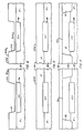
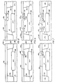
- FIG. 2 though 11 show the steps in fabricating a memory array and transistor structure according to the invention.
- the memory array with Schottky diode and fuse structure appears in the leftfiand portion of the figures and a washed emitter transistor structure incorporating a barrier layer appears in the righthand portion of the figures.
- the memory array usually occupies the major central area of the chip and the transistor is a part of the pheripheral circuitry which surrounds one or more sides of the memory array. They are shown side-by-side because the same processing steps are used to fabricate both structures simultaneously. :
- the fabrication process shown in Figure 2 starts with furnishing a P-type substrate 18 of silicon, lightly doped to have about 7-21 ohm centimeters of resistivity and a crystal axis orientation of 111.
- a thick oxide layer 20 is grown to a thickness of 1.0 micrometers or more depending upon the doping source to be used in forming the buried layer in the next step.
- Openings 22 and 24 are formed in the oxide layer 20 by photolithographic means to delineate the regions where two N-type diffusions 26 and 28 are next made.
- the dopant for the N+ diffusions may be arsenic, for example.
- the N+ diffusions 26 for the fuse link and Schottky diode structure provides a buried layer for the purpose of reducing the resistance of the cathode path of the Schottky diode, and the other N+ diffusion 28 provides a buried layer collector for the peripheral transistor.
- a small thickness 20a of oxide is shown formed over the N+ diffusion areas.
- the N+ diffusion 26 and 28 have a sheet resistance of about 20 ohms per square and a junction depth of about 3-4 micrometers.
- the oxide layers 20 and 20a are then removed in order to form an epitaxial layer 30 of N-type silicon, shown in Figure 3.
- an in situ hydrochloric etch is formed in order to ensure a clean surface on the substrate 18.
- the epitaxial layer 30 is doped with arsenic to about 45 ohm-cm. resistivity and is between 3 and 3.5 micrometers thick.
- a portion of the buried layers 26 and 28 diffuses upwardly into the epitaxial layer 30 and the lower portion diffuses deeper into the substrate 18.
- the next step is to form isolation regions for the memory elements and the peripheral transistor.
- a relatively thick oxide layer of 0.5 to 1.0 micrometer is grown on the epitaxial layer 30, after which it is masked with photoresist to provide openings in the oxide for diffusion of a P-type dopant, such as boron, to produce the isolation regions 32.
- the isolation regions 32 go deeply through the epitaxial layer 30 and into the substrate 18, as shown in Figure 4.
- an oxide is formed over the isolation regions. This oxide can be left on or it can be removed and a new oxide can be grown.
- An optional step at this stage is to diffuse a collector plug in the transistor structure. This may be done by masking, etching, and then diffussing an N + type dopant to a depth sufficient to contact the N+ buried layer region 28.
- the collector plug diffusion provides better conductivity between the collector contact to be formed at the surface of the epitaxial layer and the collector-base junction region.
- a surface oxide is formed during or after the collector plug diffusion.
- an oxide layer 34 will be present over the epitaxial layer 30 covering the isolation regions 32, as shown in Figures 4 and 5.
- the next step is to form an opening 36 in the oxide layer 34 by masking, and to diffuse a P-type dopant, such as boron, through the opening 36 to produce a base region 38 for the transistor.
- a P-type dopant such as boron
- the sheet resistance of the base region 38 may be approximately 200 ohms/sq., and the junction depth approximately 1.0 micrometer.
- a thin oxide film is formed over the base region 38.
- FIG. 6 is to form a series of openings in the oxide layer 34 through which a heavy dosage of an N-type dopant such as phosphorous or arsenic can be diffused.
- An opening 40 is provided over the base region 38 for diffusion of an N+ emitter region 42.
- a second opening 44 is provided to one side of the base region 38 for diffusion of an N+ collector contact region 46.
- a third opening 48 is provided for diffusion of an N+ cathode contact region 50 for the Schottky diode of the memory element.
- the emitter wash may be done before the contact masking step is performed to provide contacts to the base and the epitaxial layer, as shown in Figure 7, or it can be done after the contact mask step.
- any of these options (a), (b) or (c) depends primarily on the choice Schottky diodes. If a silicide Schottky diode is desired then option (b)'or (c) is chosen. If aluminum Schottky diodes are desired option (a) is chosen, along with the choise of not having silicide in the emitter. However, it is usually advantageous to have silicide wherever possible, in order to reduce or minimize contact resistance of a barrier metal to silicon as will be seen.
- silicide contacts 52 are shown deposited on the emitter region 42, on the collector contact region 46, and on the cathode contact region 50, through openings in the oxide layer 34.
- a typical composition for the silicide contacts 52 is one that is formed from 88% nickel and 12% platinum and which when alloyed with the silicon forms a ternary alloy of 50% silicon, 44% nickel, and 6% platinum.
- openings 54 and 56 are formed in the oxide layer 34.
- One opening 54 is provided over the base region 38 exposing the junction between the base region 38 in the epitaxial layer 30.
- the other opening 56 is provided over the buried layer 26 exposing the epitaxial layer 30 in the memory element region.
- the film resistivity is about 270 micro ohm-centimeters.
- the total pressure may be higher or lower, if the relative amount of nitrogen is raised or lowered accordingly.
- the titanium-tungsten-nitride film has been found to be a face-centered cubi (FCC) structure, in contrast to titanium-tungsten which is body- centered cubic (BCC).
- FCC face-centered cubi
- BCC body- centered cubic
- the atoms are located at each corner of a cube with one atom in the middle of the interior.
- a FCC or face-entered cubic crystal lattice structure the atoms are located at each corner of a cube, with one atom in the middle of each face.
- the closer packing of the atoms may account for its improved barrier metal properties over titanium-tungsten. Because it is a better barrier metal, the thickness of the film need not be as thick as titanium-tungsten for the same barrier effectiveness. Hence, a thinner film could be used. This is advantageous for a fuse material because the current density, which determines the ease of fusing is thereby increased.
- die size could be decreased relative to the use of titanium-tungsten films. The use of titanium-tungsten as a barrier metal and another thinner material as the fuse requires more processing and expense.
- negative photoresist it is necessary to use a thin aluminum coating of 50-100 nm (500-1,000 angstroms) deposited after the deposition of the TiW 2 N film to a) prevent loss of adhesion of negative photoresists which otherwise occurs during TiW 2 N etching and b) protect the surface of the TiW 2 N film from the negative photoresist processing which otherwise is more likely than positive photoresist to result in contact resistance between the aluminum deposited later for interconnects and the TiW 2 N.
- this aluminum coating could also be used in conjunction with positive photoresist. If used, etching of aluminum is done first, so that it in turn is the mask for the TiW 2 N etching.
- This bottom aluminum layer is shown at 60a froming a Schottky barrier contact with the epitaxial layer 30 at a region 61 and an ohmic contact with the fuse link 58a; at 60b forming a column line contacting the fuse link 58a; at 60c forming an ohmic contact with the cathode side of the Schottky barrier diode, and a contact for the row line to be deposited; and 60d forming a collector contact; at 60e forming an ohmic contact to the base region 38 and a Schottky barrier contact to the epitaxial layer 30; and at 60f forming an emitter contact.
- a second layer of aluminum metallization as the word lines.
- a glass layer, doped with phosphorus to prevent cracking is deposited to a thickness of about 1.0 micrometers, and masked and etched to form and opening or via.
- the glass layer is shown at 62 and the via is shown at 63.
- the second layer of aluminum is then deposited over the glass to a thickness of about 1.5 to 2.0 micrometers, and then masked and etched.
- the second aluminum layer is shown at 64 in Figure 10.
- a top layer of glass to serve as a passivation layer is deposited over the entire structure. This top layer of glass is not shown in the drawing.
- Both the intermediate glass layer and the top glass layer may be deposited from the reaction of oxygen and silane gas at substantially 400-450°C.
- Phosphorous doping of the glass is accomplished by injecting phosphine gas during glass deposition.
- the bottom aluminum contact 60a forms a Schottky barrier contact with the epitaxial layer 30 at the region 61, thereby forming the anode contact for the Schottky diode of the memory element.
- the bottom aluminum contact 60c forms the cathode contact for the Schottky barrier diode of the memory element.
- the buried N+ layer 26 provides a low resistance path for the cathode side of the Schottky diode running through the semiconductor region between the two contacts 60a and 60c.
- the Schottky barrier contact between the aluminum contact 60a and the epitaxial layer- 30 provides a Schottky barrier clamping diode connected between the base region 38 and the collector region 30 of the transistor.
- the fuse link 58a shown in Figure 11 has a rectangular shape in plan view and preferably has a notch 66 to reduce its width and thereby reduce the fuse-blowing current.
- Other well know shapes may also be used for the fuse links 58a.
- titanium-tungsten-nitride as a single conductive film to provide the dual function of a fuse link and a diffusion barrier layer in the same semiconductor chip provides reduced manufacturing complexity, with resulting cost reduction. These manufacturing efficiences can be espcially important for large scale memories where shallow emitter diffusions are encountered.
- titanium-tungsten-nitride films in accordance with the teachings of the invention can be used in other types of programmable chips such as programmable gate arrays and logic arrays and in such applications as redundancy in random access memories.
- the titanium-tungsten-nitride films can also be used to similar advantage in other types of isolated structures, such as those employing dielectric or oxide isolation.
Landscapes
- Semiconductor Memories (AREA)
- Read Only Memory (AREA)
- Bipolar Transistors (AREA)
- Electrodes Of Semiconductors (AREA)
Claims (11)
Applications Claiming Priority (2)
| Application Number | Priority Date | Filing Date | Title |
|---|---|---|---|
| US06/371,147 US4491860A (en) | 1982-04-23 | 1982-04-23 | TiW2 N Fusible links in semiconductor integrated circuits |
| US371147 | 1989-06-26 |
Publications (3)
| Publication Number | Publication Date |
|---|---|
| EP0092871A2 EP0092871A2 (de) | 1983-11-02 |
| EP0092871A3 EP0092871A3 (en) | 1985-09-04 |
| EP0092871B1 true EP0092871B1 (de) | 1990-02-07 |
Family
ID=23462680
Family Applications (1)
| Application Number | Title | Priority Date | Filing Date |
|---|---|---|---|
| EP83200562A Expired - Lifetime EP0092871B1 (de) | 1982-04-23 | 1983-04-19 | Integrierte Halbleiterschaltungen und Verfahren zur Herstellung |
Country Status (4)
| Country | Link |
|---|---|
| US (1) | US4491860A (de) |
| EP (1) | EP0092871B1 (de) |
| JP (1) | JPS5948554B2 (de) |
| DE (1) | DE3381215D1 (de) |
Cited By (2)
| Publication number | Priority date | Publication date | Assignee | Title |
|---|---|---|---|---|
| US5763898A (en) | 1990-04-12 | 1998-06-09 | Actel Corporation | Above via metal-to-metal antifuses incorporating a tungsten via plug |
| US5780323A (en) | 1990-04-12 | 1998-07-14 | Actel Corporation | Fabrication method for metal-to-metal antifuses incorporating a tungsten via plug |
Families Citing this family (44)
| Publication number | Priority date | Publication date | Assignee | Title |
|---|---|---|---|---|
| JPS60169169A (ja) * | 1984-02-13 | 1985-09-02 | Fujitsu Ltd | 半導体装置の製造方法 |
| US4920071A (en) * | 1985-03-15 | 1990-04-24 | Fairchild Camera And Instrument Corporation | High temperature interconnect system for an integrated circuit |
| US4811078A (en) * | 1985-05-01 | 1989-03-07 | Texas Instruments Incorporated | Integrated circuit device and process with tin capacitors |
| US4782032A (en) * | 1987-01-12 | 1988-11-01 | Itt Gallium Arsenide Technology Center, A Division Of Itt Corporation | Method of making self-aligned GaAs devices having TiWNx gate/interconnect |
| US4956308A (en) * | 1987-01-20 | 1990-09-11 | Itt Corporation | Method of making self-aligned field-effect transistor |
| US4728534A (en) * | 1986-08-04 | 1988-03-01 | Motorola, Inc. | Thick film conductor structure |
| US5436496A (en) * | 1986-08-29 | 1995-07-25 | National Semiconductor Corporation | Vertical fuse device |
| DE3641299A1 (de) * | 1986-12-03 | 1988-06-16 | Philips Patentverwaltung | Integrierte halbleiter-schaltung mit mehrlagenverdrahtung |
| US4935801A (en) * | 1987-01-27 | 1990-06-19 | Inmos Corporation | Metallic fuse with optically absorptive layer |
| DE3714647C2 (de) * | 1987-05-02 | 1993-10-07 | Telefunken Microelectron | Integrierte Schaltungsanordnung |
| JPS6417555U (de) * | 1987-07-22 | 1989-01-27 | ||
| US4787958A (en) * | 1987-08-28 | 1988-11-29 | Motorola Inc. | Method of chemically etching TiW and/or TiWN |
| NL8800220A (nl) * | 1988-01-29 | 1989-08-16 | Philips Nv | Werkwijze voor het vervaardigen van een halfgeleiderinrichting, waarbij een metalen geleiderspoor op een oppervlak van een halfgeleiderlichaam wordt gebracht. |
| US4795499A (en) * | 1988-03-28 | 1989-01-03 | Ridenour Ralph Gaylord | Duct mount sensor assembly |
| US4927505A (en) * | 1988-07-05 | 1990-05-22 | Motorola Inc. | Metallization scheme providing adhesion and barrier properties |
| US4880708A (en) * | 1988-07-05 | 1989-11-14 | Motorola, Inc. | Metallization scheme providing adhesion and barrier properties |
| DE3930655A1 (de) * | 1988-09-13 | 1990-03-22 | Mitsubishi Electric Corp | Halbleitervorrichtung mit vielschichtig gestapelter verbindungsschicht und verfahren zu deren herstellung |
| US5015604A (en) * | 1989-08-18 | 1991-05-14 | North American Philips Corp., Signetics Division | Fabrication method using oxidation to control size of fusible link |
| US5211807A (en) * | 1991-07-02 | 1993-05-18 | Microelectronics Computer & Technology | Titanium-tungsten etching solutions |
| US5241496A (en) * | 1991-08-19 | 1993-08-31 | Micron Technology, Inc. | Array of read-only memory cells, eacch of which has a one-time, voltage-programmable antifuse element constructed within a trench shared by a pair of cells |
| US5244836A (en) * | 1991-12-30 | 1993-09-14 | North American Philips Corporation | Method of manufacturing fusible links in semiconductor devices |
| EP0558176A1 (de) * | 1992-02-26 | 1993-09-01 | Actel Corporation | Metall-Metall-Antischmelzsicherung mit verbesserter Diffusionsbarriere-Schicht |
| KR100272019B1 (ko) * | 1992-04-28 | 2000-12-01 | 요트.게.아. 롤페즈 | 표면에 tixw1-x 장벽층이 제공되는 반도체 몸체를 갖는 반도체 장치 및 그 제조 방법 |
| US5834824A (en) * | 1994-02-08 | 1998-11-10 | Prolinx Labs Corporation | Use of conductive particles in a nonconductive body as an integrated circuit antifuse |
| US5917229A (en) * | 1994-02-08 | 1999-06-29 | Prolinx Labs Corporation | Programmable/reprogrammable printed circuit board using fuse and/or antifuse as interconnect |
| US5808351A (en) * | 1994-02-08 | 1998-09-15 | Prolinx Labs Corporation | Programmable/reprogramable structure using fuses and antifuses |
| US5726482A (en) * | 1994-02-08 | 1998-03-10 | Prolinx Labs Corporation | Device-under-test card for a burn-in board |
| TW279229B (en) * | 1994-12-29 | 1996-06-21 | Siemens Ag | Double density fuse bank for the laser break-link programming of an integrated-circuit |
| US5962815A (en) * | 1995-01-18 | 1999-10-05 | Prolinx Labs Corporation | Antifuse interconnect between two conducting layers of a printed circuit board |
| US5906042A (en) * | 1995-10-04 | 1999-05-25 | Prolinx Labs Corporation | Method and structure to interconnect traces of two conductive layers in a printed circuit board |
| US5767575A (en) * | 1995-10-17 | 1998-06-16 | Prolinx Labs Corporation | Ball grid array structure and method for packaging an integrated circuit chip |
| US5872338A (en) * | 1996-04-10 | 1999-02-16 | Prolinx Labs Corporation | Multilayer board having insulating isolation rings |
| US5933714A (en) * | 1997-01-08 | 1999-08-03 | Siemens Aktiengesellschaft | Double density fuse bank for the laser break-link programming of an integrated circuit |
| US6015505A (en) * | 1997-10-30 | 2000-01-18 | International Business Machines Corporation | Process improvements for titanium-tungsten etching in the presence of electroplated C4's |
| US6034427A (en) * | 1998-01-28 | 2000-03-07 | Prolinx Labs Corporation | Ball grid array structure and method for packaging an integrated circuit chip |
| US6277674B1 (en) | 1998-10-02 | 2001-08-21 | Micron Technology, Inc. | Semiconductor fuses, methods of using the same, methods of making the same, and semiconductor devices containing the same |
| US20070190751A1 (en) * | 1999-03-29 | 2007-08-16 | Marr Kenneth W | Semiconductor fuses and methods for fabricating and programming the same |
| US6646912B2 (en) * | 2001-06-05 | 2003-11-11 | Hewlett-Packard Development Company, Lp. | Non-volatile memory |
| US6927472B2 (en) * | 2001-11-14 | 2005-08-09 | International Business Machines Corporation | Fuse structure and method to form the same |
| US20040038458A1 (en) * | 2002-08-23 | 2004-02-26 | Marr Kenneth W. | Semiconductor fuses, semiconductor devices containing the same, and methods of making and using the same |
| US6972470B2 (en) * | 2004-03-30 | 2005-12-06 | Texas Instruments Incorporated | Dual metal Schottky diode |
| DE102005052087A1 (de) * | 2005-10-28 | 2007-05-03 | Kmw Kaufbeurer Mikrosysteme Wiedemann Gmbh | Sensor |
| US20070205430A1 (en) * | 2006-03-03 | 2007-09-06 | Collins David S | Method and structure of refractory metal reach through in bipolar transistor |
| WO2022137652A1 (ja) * | 2020-12-25 | 2022-06-30 | 日立Astemo株式会社 | 車載用電子制御装置 |
Family Cites Families (5)
| Publication number | Priority date | Publication date | Assignee | Title |
|---|---|---|---|---|
| US28481A (en) * | 1860-05-29 | Mosaic veneer | ||
| USRE28481E (en) | 1972-01-20 | 1975-07-15 | Semiconductor structure with fusible link and method | |
| US4179533A (en) * | 1978-04-25 | 1979-12-18 | The United States Of America As Represented By The Secretary Of The Navy | Multi-refractory films for gallium arsenide devices |
| US4209894A (en) * | 1978-04-27 | 1980-07-01 | Texas Instruments Incorporated | Fusible-link semiconductor memory |
| FR2530383A1 (fr) * | 1982-07-13 | 1984-01-20 | Thomson Csf | Circuit integre monolithique comprenant une partie logique schottky et une memoire programmable a fusibles |
-
1982
- 1982-04-23 US US06/371,147 patent/US4491860A/en not_active Expired - Lifetime
-
1983
- 1983-04-19 EP EP83200562A patent/EP0092871B1/de not_active Expired - Lifetime
- 1983-04-19 DE DE8383200562T patent/DE3381215D1/de not_active Expired - Lifetime
- 1983-04-20 JP JP58068493A patent/JPS5948554B2/ja not_active Expired
Cited By (2)
| Publication number | Priority date | Publication date | Assignee | Title |
|---|---|---|---|---|
| US5763898A (en) | 1990-04-12 | 1998-06-09 | Actel Corporation | Above via metal-to-metal antifuses incorporating a tungsten via plug |
| US5780323A (en) | 1990-04-12 | 1998-07-14 | Actel Corporation | Fabrication method for metal-to-metal antifuses incorporating a tungsten via plug |
Also Published As
| Publication number | Publication date |
|---|---|
| DE3381215D1 (de) | 1990-03-15 |
| US4491860A (en) | 1985-01-01 |
| JPS5948554B2 (ja) | 1984-11-27 |
| JPS58212163A (ja) | 1983-12-09 |
| EP0092871A3 (en) | 1985-09-04 |
| EP0092871A2 (de) | 1983-11-02 |
Similar Documents
| Publication | Publication Date | Title |
|---|---|---|
| US4491860A (en) | TiW2 N Fusible links in semiconductor integrated circuits | |
| US4569121A (en) | Method of fabricating a programmable read-only memory cell incorporating an antifuse utilizing deposition of amorphous semiconductor layer | |
| US4569120A (en) | Method of fabricating a programmable read-only memory cell incorporating an antifuse utilizing ion implantation | |
| US4499557A (en) | Programmable cell for use in programmable electronic arrays | |
| KR100201182B1 (ko) | 반도체집적회로장치 | |
| US5739564A (en) | Semiconductor device having a static-random-access memory cell | |
| US5144404A (en) | Polysilicon Schottky clamped transistor and vertical fuse devices | |
| US4229757A (en) | Programmable memory cell having semiconductor diodes | |
| EP0047133B1 (de) | Halbleiterspeicher hoher Dichte und Verfahren zu dessen Herstellung | |
| US5130267A (en) | Split metal plate capacitor and method for making the same | |
| US5466638A (en) | Method of manufacturing a metal interconnect with high resistance to electromigration | |
| CA1121070A (en) | Method for forming semiconductor contacts | |
| US5059555A (en) | Method to fabricate vertical fuse devices and Schottky diodes using thin sacrificial layer | |
| JPS587840A (ja) | 半導体集積回路 | |
| EP0305296B1 (de) | Halbleiterschichtstruktur mit einer Aluminium-Silizium-Legierungsschicht | |
| EP0058124B1 (de) | Anordnung von Schottkydioden aus polykristallinem Silizium und Verfahren zur Herstellung | |
| US4665424A (en) | Semiconductor device | |
| CA1205574A (en) | Ion implanted memory cells for high density ram | |
| US4908679A (en) | Low resistance Schottky diode on polysilicon/metal-silicide | |
| US5212102A (en) | Method of making polysilicon Schottky clamped transistor and vertical fuse devices | |
| US4516223A (en) | High density bipolar ROM having a lateral PN diode as a matrix element and method of fabrication | |
| US4628339A (en) | Polycrystalline silicon Schottky diode array | |
| EP0621631A1 (de) | Verfahren zur Herstellung von Widerständen für integrierte Schaltkreise unter Verwendung von Gräben | |
| CA1205577A (en) | Semiconductor device | |
| US6544830B2 (en) | Method of manufacturing a semiconductor device with multiple emitter contact plugs |
Legal Events
| Date | Code | Title | Description |
|---|---|---|---|
| PUAI | Public reference made under article 153(3) epc to a published international application that has entered the european phase |
Free format text: ORIGINAL CODE: 0009012 |
|
| AK | Designated contracting states |
Designated state(s): DE FR GB |
|
| PUAL | Search report despatched |
Free format text: ORIGINAL CODE: 0009013 |
|
| AK | Designated contracting states |
Designated state(s): DE FR GB |
|
| 17P | Request for examination filed |
Effective date: 19860407 |
|
| 17Q | First examination report despatched |
Effective date: 19870911 |
|
| GRAA | (expected) grant |
Free format text: ORIGINAL CODE: 0009210 |
|
| AK | Designated contracting states |
Kind code of ref document: B1 Designated state(s): DE FR GB |
|
| REF | Corresponds to: |
Ref document number: 3381215 Country of ref document: DE Date of ref document: 19900315 |
|
| ET | Fr: translation filed | ||
| PLBE | No opposition filed within time limit |
Free format text: ORIGINAL CODE: 0009261 |
|
| STAA | Information on the status of an ep patent application or granted ep patent |
Free format text: STATUS: NO OPPOSITION FILED WITHIN TIME LIMIT |
|
| 26N | No opposition filed | ||
| REG | Reference to a national code |
Ref country code: FR Ref legal event code: CD |
|
| REG | Reference to a national code |
Ref country code: FR Ref legal event code: CD |
|
| PGFP | Annual fee paid to national office [announced via postgrant information from national office to epo] |
Ref country code: DE Payment date: 20010620 Year of fee payment: 19 |
|
| REG | Reference to a national code |
Ref country code: GB Ref legal event code: IF02 |
|
| PGFP | Annual fee paid to national office [announced via postgrant information from national office to epo] |
Ref country code: FR Payment date: 20020426 Year of fee payment: 20 |
|
| PGFP | Annual fee paid to national office [announced via postgrant information from national office to epo] |
Ref country code: GB Payment date: 20020430 Year of fee payment: 20 |
|
| PG25 | Lapsed in a contracting state [announced via postgrant information from national office to epo] |
Ref country code: DE Free format text: LAPSE BECAUSE OF NON-PAYMENT OF DUE FEES Effective date: 20021101 |
|
| PG25 | Lapsed in a contracting state [announced via postgrant information from national office to epo] |
Ref country code: GB Free format text: LAPSE BECAUSE OF EXPIRATION OF PROTECTION Effective date: 20030418 |
|
| REG | Reference to a national code |
Ref country code: GB Ref legal event code: PE20 |