EP0092429A2 - Sonderinstruktionsverarbeitungseinheit für Datenverarbeitungssystem - Google Patents
Sonderinstruktionsverarbeitungseinheit für Datenverarbeitungssystem Download PDFInfo
- Publication number
- EP0092429A2 EP0092429A2 EP83302213A EP83302213A EP0092429A2 EP 0092429 A2 EP0092429 A2 EP 0092429A2 EP 83302213 A EP83302213 A EP 83302213A EP 83302213 A EP83302213 A EP 83302213A EP 0092429 A2 EP0092429 A2 EP 0092429A2
- Authority
- EP
- European Patent Office
- Prior art keywords
- processor
- processing unit
- instruction
- central processing
- data
- Prior art date
- Legal status (The legal status is an assumption and is not a legal conclusion. Google has not performed a legal analysis and makes no representation as to the accuracy of the status listed.)
- Granted
Links
Images


Classifications
-
- G—PHYSICS
- G06—COMPUTING; CALCULATING OR COUNTING
- G06F—ELECTRIC DIGITAL DATA PROCESSING
- G06F9/00—Arrangements for program control, e.g. control units
- G06F9/06—Arrangements for program control, e.g. control units using stored programs, i.e. using an internal store of processing equipment to receive or retain programs
- G06F9/30—Arrangements for executing machine instructions, e.g. instruction decode
- G06F9/38—Concurrent instruction execution, e.g. pipeline, look ahead
- G06F9/3877—Concurrent instruction execution, e.g. pipeline, look ahead using a slave processor, e.g. coprocessor
Definitions
- This invention relates to electronic digital data processing systems incorporating a special instruction processor such as a floating point accelerator processor. More specifically, the invention relates to a new and improved interconnection arrangement between the floating point processor and a central processor unit.
- a digital data processing system comprises three elements: namely, a memory element, an input/output element, and a processor element.
- the memory element stores information in addressable storage locations, with each location having a unique address.
- the information stored in the memory includes data, or "operands", and instructions for processing the operands.
- the processor element transfers information to and from the memory element, interprets the information as either instructions or operands and processes the operands in accordance with the associated instructions.
- the input/output element under control of the processor unit, also communicates with the memory element in order to transfer operands and instructions into the system and obtain processed data from it.
- Operands processed by a processing unit may take a number of forms. In many processing operations, operands are in the form of integers or whole numbers. In other operations, operands are in a floating point format, that is, in what is typically known as "scientific notation". In this form, an operand has two parts, including an exponent and a mantissa. In a binary-based system used in most computers, the mantissa is a fraction with a binary point to the immediate left of the most significant digit, and the exponent represents the power of two to which the mantissa must be taken to obtain the value of the number. Each of the mantissa and the exponent may contain a sign, either positive or negative.
- operands for trigonometric functions may have a different form from both integer and floating point operands.
- some trigonometric functions may be repetitive for each multiple of three hundred and sixty degrees, if the operands are expressed in degrees, or may represent or require specific operations with respect to "pi" if the operands are expressed in radian notation.
- other special operand notations are conceivable.
- Each of these special classes of operands may require special handling by the processor.
- the central processing init contains special control circuitry for executing the special instructions.
- floating point instructions usually require significantly nore time to complete than do instructions on conventional integer operands.
- the addition of floating point instructions can significantly increase the overall time to complete a given program.
- the operands are processed using subroutines comprising sets of the machine instructions to implement the floating point functions.
- the central processor unit merely uses a floating point instruction as an instruction directing the processor to execute the appropriate subroutine.
- This approach enables the functions performed by the special class of instructions to be altered relatively simply.
- this approach is considerably slower than the hardware approach, as the mantissas and exponents of the operands must be handled separately.
- each module can execute all of the instructions on the different classes of operands, or specific modules may be assigned to process instructions on classes of operands. In either case, each module operates independently by retrieving data from or storing data in the memory unit directly.
- a controlling module may retrieve the instructions in seriatum and transfer it to either an idle module, or to the module designed to execute that operation.
- the modules operate in parallel, they may operate simultaneously, within the constraint that normally one instruction cannot be executed until a previous instruction has been executed. While the time required to perform a single operation is about the same as in the prior hardware approach, the parallel nature of the module significantly reduces the time to execute a program contained in the special instructions, as a free module may be used to process interrupts. However, as each module must be capable of operating independently, circuit redundancy is necessary. Each module usually performs only one function, and is not readily converted into other functions.
- a separate module termed a "floating point accelerator” processes instructions in conjunction with floating point operands.
- the instruction indicates whether the operand is floating point or integer, and if the instruction indicates that the operand is floating point, the central processor unit passes the instruction to the floating point accelerator.
- the floating point accelerator then decodes the instruction, and requests the central processing unit to retrieve operands from the memory unit for memory, and to store the processed data in the memory. While this approach allows the central processing unit the freedom to process such things as interrupts while the floating point accelerator is in the process of executing the floating point instruction, the required interaction between the central processing unit and the floating point accelerator unnecessarily complicates both units.
- this invention provides a new and improved interconnection arrangement between the central processing unit and a processing module for processing a special class of instructions that operate on a uniquely defined class of operands.
- the central processing unit retrieves all of the instructions, in series, in a conventional manner, and decodes the instructions. An image of each instruction is passed to the special instruction processor.
- the central processing unit retrieves the data words comprising the operands from the memory and passes them to the special instruction processor.
- the special instruction processor After receiving the instruction the special instruction processor also decodes the instruction and proceeds to receive the data words comprising the operands. The special instruction processor then processes the operands in a conventional manner, and prepares to transmit the results of processing, namely the processed data and the condition codes, back to the central processing unit. When the central processing unit is signalled by the special instruction processor that it has finished processing, it signals the special instruction processor to transmit the data. The special instruction processor then transmits the data and the condition codes. The central processing unit then can transmit the processed data back into storage in the memory.
- the invention provides certain maintenance and diagnostic features in which the central processing unit can force the special instruction processor to a selected state, and it can also determine the state of the special instruction processor.
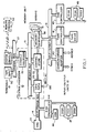
- the basic elements of a data processing system that embody this invention comprise a central processor unit 10, memory unit 11, and input/output units 12, which include terminals 13.
- the central processor unit communicates directly with certain of the input/output units 12 over an accelerator bus 14.
- the central processor unit 10 communicates with memory unit 11 over a memory bus 15, and the memory unit in turn communicates directly with others of input/output units 12 over an input/output bus 16.
- the central processor unit 10 communicates with terminals 13 over a terminal bus 17.
- the central processor unit comprises a data processor 2g, and control store 21 which are connected to memory bus 15, and a console processor 22.
- the console processor receives signals from terminal bus 17, and transfers them through control store 21 to data processor 20.
- Data processor 2g then operates on the information from console processor 22 and may transfer the information to the memory unit 11 for future processing, or it may process information directly.
- data processor 20 may transfer information through control store 21 to the console processor 22, which may then transmit the information to terminal bus 17 for transfer to one of terminals 13.
- the data processor also performs all communications over the accelerator bus 14 with those input/output units 12 connected thereto. The communications with input/output units 12 over accelerator bus 14 are described in copending U.S. Patent Application Serial No. (Attorney's Docket 83-277), filed
- the data path communicates directly with the memory unit 11 over memory bus 15, and indirectly with the input/output bus 16 through memory unit 11.
- the control store 21 contains all of the microinstruction sequences that are used for processing the instructions that are received and executed by data processor 20, and steps through the microinstruction sequences based on sequencing information from the data processor and timing information from a timing signal generator which it maintains.
- Memory unit 11 contains a memory controller 30 having one connection, or port, to memory bus 15, and a second connected to input/output bus 16.
- One or more memory arrays 31 connect to memory controller 30 and contain the addressable memory storage locations that may be accessed directly by the memory controller.
- a floating point accelerator processor 23 may be connected to accelerator bus 14.
- a floating point accelerator processor 23 useful in the data processing system of FIG. 1, and the accelerator bus 14 are described herein.
- Floating point accelerator processor 23 receives floating point instructions Erom data processor 20 and is specially designed to process such instructions generally more rapidly than data processor 20 would normally be able to.
- a communications adapter 40 can connect to synchronous and/or asynchronous data communications lines to transfer information over, for example, conventional telephone lines, or to enable connection of the data processing system as one element in a local distributed processing network. Specific signals for the synchronous and asynchronous connection to communications adapter 40 are not shown; however, such signals would depend on the particular signal protocols used in such transmission, and are not a part of this invention.
- the communications adapter 40 normally would include circuitry for buffering information during the synchronous or asynchronous transfers, and for generating control signals over the synchronous and asynchronous communications paths to enable the information to be transferred.
- the communications adapter 40 also contains circuitry for transferring information over input/output bus 16. Since the communications adapter forms io part of this invention, it will not be described further ierein.
- Three other input/output units 12 provide a secondary storage facility for the data processing system. They include a tape controller 41 connected to a tape drive 42, and two disc controllers 43 and 44. Disc controller 43 is :onnected to a plurality of disc drives 45, while disc :ontroller 44 may be connected to a disc drive 46 and to a plurality of disc drives 47. Disc controller 44 is connected :o accelerator bus 14, and is described in the aforementioned copending U.S. Patent Application Serial No. (Attorney's Docket No. 83-277), filed Units 41 and 43, and their respective storage elements may be constructed as described in U.S. Patent No. 3,999,163.
- the input/output bus is constructed in accordance with U.S. Patent No. 3,710,324, which describes in detail the signals required to transfer information thereover. These 3 ignals are only briefly described herein, and reference should be made to that patent for a detailed explanation.
- Terminals 13 may include a tape drive 50, or a system console 51, which are directly connected to terminal bus 17.
- An optional remote console 52 may be provided to transfer signals with terminal bus 17 over telephone lines through conventional modems (not shown).
- the remote console 52 can be used for remote diagnosis of system failures or for remote maintenance.
- the tape drive 5V may be used for local maintenance or for transferring information into or out of the system.
- the system console may be used to provide direct operator control of the system, and may permit the operator to turn the system on or off, to initialize the system, and to step through a program sequence step-by-step.
- Information is intelligence that controls and provides the basis for data processing. It includes address, data, control and status information.
- Data includes information which is the object of or result of processing.
- Address information identifies a particular storage location in which other information, such as data information, control or status information or other address information, is stored.
- Control information identifies particular operations to be performed. It includes commands between units of a data processing system that certain operations be performed, instructions to be performed by the central processor 10 or floating point accelerator processor 23, and it also includes information that modifies a unit's performance of an operation or execution of an instruction so as to enable certain actions to occur or disable actions from occurring.
- An "instruction” is a step in a program that is executed by the central processor unit 10 or floating point accelerator processor 23. Each step may be executed by the respective processor executing one or more microinstructions. Each microinstruction is stored in a specific location, which is identified as a micro-address. Other units, for example, nemory controller 3g, also perform operations in response to and as defined in sequences of microinstructions.
- Status information identifies the condition of various signals generated by a unit at various times during the processing of an operation or execution of an instruction.
- FIG. 2 illustrates, in general block diagram form, portions of central processor 10, including data processor 20 and control store 21, that may be useful in the data processing system of FIG. 1.
- Data processor 20 includes a data path 60 that includes an arithmatic logic unit and a plurality of general purpose registers (not shown).
- one of the general purpose registers is used as a program counter to identify the storage location in memory containing the next instruction to be executed by the processor 10 and another register is used as a stack pointer used during the servicing of interrupts and subroutines, as described in U.S. Patent No. 3,710,324.
- the data path 60 receives information from, or transfers information to, the accelerator bus 14, the memory bus 15, or from a plurality of console registers 61 that in turn receive and store information from, or transfer information to, console processor 22 over a console bus 62.
- Operations performed by data path 60 are controlled by instructions stored in an instruction buffer 63, which receives each instruction fetched from memory unit 11 identified by the program counter register in data path 60.
- the operations performed by data path 60 can be controlled by an interrupt processor 64 which receives requests for interrupt service from accelerator bus 14, console bus 62 (through console registers 61) and from the input/output bus 16.
- the interrupt processor 64 also receives the interrupt priority level at which the processor 10 is then operating and, if the interrupt request has a higher priority, acknowledges the interrupt and causes the processor 10 to service the interrupt request.
- a nicrosequencer 65 generates a microaddress that is used by a nicro-control store 66 in control store 21 to access a nicroinstruction depending on the instructions stored in instruction buffer 63, or the interrupt being serviced by interrupt processor 64.
- the microsequencer 65 generates the nicroaddress in response to the particular instruction in instruction buffer 63 then being processed, and the acknowledgement of an interrupt by interrupt processor 64, as well as timing signals generated by a clock generator 67 in control store 21.
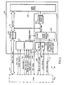
- FIG. 3 A general block diagram of a floating point accelerator 23 is shown in FIG. 3.
- a floating point instruction as transferred to the floating point accelerator by the central processing unit 10, specifically by the data path 20, is received in an instruction decoder 101.
- One specific embodiment of floating point accelerator 23 is microprogrammed.
- the instruction decoder is thus connected to a microaddress sequencer 102 in a conventional manner, which in turn supplies microaddresses to a control store 103.
- the control store contains microinstructions that control the operations of floating point accelerator 23, including a data path 104.
- the data path contains operand storage registers and an arithmetic and logic unit that processes the operands that are received from the central processor unit 10 through a transceiver buffer 105.
- the microaddress sequencer 102 uses conventional microinstruction addressing techniques, supplies a "next microaddress" to the control store 103.
- the microaddress sequencer 102 also receives signals from the control store 103 and from a branch logic 106, and generates the next microaddress that is then transmitted to the control store.
- the control store thus generates microinstructions that control the data path logic 104 based on a predetermined microinstruction sequence.
- the specific sequence is determined by the instruction from central processor unit 10, as modified by certain conditions in the floating point accelerator 23 as reflected by branch logic 106.
- Data path logic 104 also uses conventional data paths to process floating point instructions.
- the data path contains separate data paths for the exponent and for the mantissa, and operates on each according to the microinstructions from control store 103.
- the data path Logic comprises conventional AMD 2901 bit slice nicroprocessors sold by Advanced Micro Devices, Inc.
- Floating point accelerator 23 also includes interface control circuitry 107 that also receives signals from the central processing unit and assists in synchronizing the transfer of operands and processed data between the central processor unit 10 and floating point accelerator 23.
- interface control circuitry 107 receives signals from the central processing unit and assists in synchronizing the transfer of operands and processed data between the central processor unit 10 and floating point accelerator 23.
- the central processing unit serially retrieves each instruction from the memory unit 11. Each instruction is loaded into instruction buffer 63 (FIG. 2). The instruction buffer and the associated processor then decode the instruction. If the instruction is a floating point instruction, that is, an instruction that indicates that the operands are in floating point format, it transmits the instruction to the floating point accelerator over the BUS IB D(7:0) 108 (FIG 3.), simultaneously asserting a synchronizing IRD STATE instruction read signal 109.
- the instruction processor 63 (FIG. 2) in central processor unit 10 further decodes the instruction and proceeds to retrieve the operands from the memory unit 11.
- Each instruction may require one or more operands, and an operand may comprise one or more data words in the memory depending on the required degree of arithmetic precision, each data word requiring a memory retrieval.
- Each data word is transferred through the ALU 60 (FIG. 2) of the central processor unit 10, and transmitted over BUS Y D(31:00) 110 (FIG 3), the data section of accelerator bus 14.
- BUS Y (D31:00) 110 is synchronized to the assertion of a CPU DATA AVAIL CPU data available signal 111.
- the floating point accelerator 23 receives each data word, in buffer 105, and transfers it onto a BUS FPA floating point accelerator bus.
- the control store 103 determines which registers of data path logic 104 each transferred data word is to be stored in, depending on whether the word forms part of the mantissa or the exponent.
- the instruction previously transferred into instruction decoder 101 also identifies the number of operands and the number of data words, required to process the instruction.
- Control store 103 causes the data words to be transferred through buffer 105 and into registers in data path logic 104 in accordance with the number of words to be received. After all the operands have been received, the data path logic 104, under control of control store 103, executes the instruction in a conventional manner.
- control store 103 transmits an ACC SYNC accelerator synchronization signal over line 12V (FIG. 3) to central processor unit 10.
- This signal is a signal in the microinstruction generated by control store 103 following execution of each instruction.
- the central processing unit 10 receives the signal and services it as an interrupt service request. When it is ready to receive the processed data from the floating point accelerator, it asserts a READ PORT signal on a line 121 and a SEL ACC IN select accelerator in signal on line 122. Since several units may be connected to accelerator bus 14, the SEL ACC IN select accelerator in signal serves to enable the floating point accelerator 23 to transmit on the BUS Y D(31:00) 11V and prevents other attached units from transmitting data over those lines.
- the floating point accelerator 23 transmits the condition codes and data words comprising the processed data from data path logic 104 across BUS FPA 112 through buffer 105 and across BUS Y D(31:00) 110.
- the central processor unit 10, specifically data path 20, receives the condition codes and data words and transmits them to the memory unit 11.
- the arrangement according to the invention provides a much less complex interconnection arrangement between central processor unit 10 and a floating point accelerator 23.
- the special instruction in one specific embodiment of a floating point instruction, is transmitted by the central processing unit 10 to floating point accelerator processor 23, and the operands are then automatically and sequentially retrieved by data path 2g and transmitted directly to floating point accelerator 23 with no further interaction between them.
- the floating point accelerator signals the central processing unit.
- the central processing unit When the central processing unit is ready to receive the processed data, it signals the floating point accelerator, which responds with successive data words.
- Both the central processor unit and floating point accelerator determine the number of data words to be transferred in both directions, as operands and processed data, based on the contents of the instructions. Therefore, the only communication back and forth as to the number of data words to be transferred is by way of the instruction. This simplifies the floating point accelerator and the communications therebetween.
- the central processing unit 10 and floating point accelerator also provide maintenance and diagnosing features in which the central processor unit 10 may transmit a "next microaddress" to the floating point accelerator control store 103 to place the control store in a specific and known address condition. Furthermore, the central processor unit may read, or retrieve, the "next microaddress" that is supplied by microaddress sequencer 102 to control store 103.
- the central processor unit forces the control store 103 to a known address condition will be described in connection with FIG. 3.
- the central processor unit transmits a microaddress over BUS Y D(31:00) 110, and asserts a TRAP ACC trap accelerator signal on line 123.
- the TRAP ACC trap accelerator signal is received in control circuitry 107, which inhibits the microaddress sequencer 102 from transmitting a next microaddress onto the control store, and enables the signals on the BUS Y D(31:00) to be transmitted through buffer 105 and to the "next microaddress" input to control store 103.
- the control store 103 then transmits the microinstruction identified by the supplied signals, forcing a shift to the sequence defined by the address transmitted on BUS Y (D31:00) 110.
- the central processor unit 10 retrieves the microaddress transmitted by microaddress sequencer 102 will be explained in connection with FIG. 3.
- the central processor unit first transmits a READ ACC UPC read accelerator microprogram counter signal on line 124 to control circuitry 107. This conditions the floating point accelerator 23 to transfer the next microaddress generated by microaddress sequencer 102 to transceiver 132 in buffer 105.
- the central processor unit asserts the READ PORT signal on line 121.
- the "next microaddress” is transmitted through buffer 105 onto BUS Y D(31:00) in synchronism with the control store's assertion of the ACC SYNC accelerator sync signal on line 120 from control store 103.
- the "next microaddress” is removed from the BUS Y D(31:00) 110 and the floating point accelerator 23 returns to normal operation.
- FIG. 4 depicts certain circuitry in control 107 that enables the floating point accelerator 23 to receive the READ PORT, SEL ACC IN select accelerator in signal, READ ACC UPC read accelerator microprogram counter signal, and TRAP ACC trap accelerator signal and enables it to transmit and receive the associated signals over BUS Y D(31:00).
- the READ PORT and SEL ACC IN select accelerator in signals are received in the control circuit 107 and coupled to an AND gate 131.
- the coincidence of these signals causes the assertion of an CPU RCV DATA central processing unit receive data signal which is coupled to branch logic 106.
- rhis causes the microaddress sequencer 102 to shift control store 103 to a sequence that causes the floating point accelerator 23 to transmit processed data and the condition codes to central processor unit 10.
- This signal also conditions a transceiver 132 in buffer 105 between BUS FPA 112 and BUS Y D(31:00) 110 to transmit data from floating point accelerator 23 to central processor unit 10.
- the CPU RCV DATA central processing unit receive data signal also energizes OR gates 134, 135 and one input to AND gate 136, which is also energized by a CPU PH0 clocking signal from central processor unit 10, and an ALLOW CPU Y BUS signal from control store 103 to enable transceiver 132.
- Transceiver 132 is thus conditioned to transfer signals from BUS Y D(31:00) 110 to BUS FPA 112 through buffer 105.
- the transceiver is enabled by the TRAP ACC trap accelerator signal through OR gates 134 and 135, and AND gate 136 when the CPU PH0 timing signal and ALLOW CPU Y BUS signal from control store 103 are asserted.
- the TRAP ACC trap accelerator signal also causes a flip-flop 140 to be set through AND gate 141 at the coincidence of the CPU PH0 and CLK OFF timing signals.
- the setting of flip-flop 140 causes a FORCE UADRS force microaddress signal to be asserted. As shown in FIG. 3, this signal is transmitted from control 107 to microaddress sequencer 102. When the FORCE UADRS force microaddress signal is asserted, the address from microaddress sequencer 102 is not transmitted to control store 103.
- the FORCE UADRS force microaddress signal enables a transceiver 141 to transfer a next microaddress from the BUS FPA 112 to control store 103.
- the transceivers 141 are enabled through an OR gate 143.
- the flip-flop 140 is reset at the assertion of the next CPU PH0 timing signal but through an AND gate 144.
- the control 107 receives the READ ACC UPC read accelerator microprogram counter signal in a flip-flop 150. which generates a READ UADRS read microaddress signal.
- This READ UADRS read microaddress signal is coupled through OR gate 143 to enable transceiver 142.
- the transceiver 142 is conditioned to transmit the next microaddress signal from microaddress sequencer lg2 onto BUS FPA 112.
- the flip-flop 150 is then reset through AND gate 151 at the next CPU PH g clocking signal.
- FIG. 5 depicts detailed sequences of the operations of transferring instructions, operands, and processed data, as well as microaddresses between CPU 10 and floating point accelerator 23.
- the sequences depicted in FIG. 5 are self- explanatory and a detailed description of these operations is not required here for an understanding of the invention.
Applications Claiming Priority (2)
| Application Number | Priority Date | Filing Date | Title |
|---|---|---|---|
| US06/370,390 US4509116A (en) | 1982-04-21 | 1982-04-21 | Special instruction processing unit for data processing system |
| US370390 | 1999-08-06 |
Publications (3)
| Publication Number | Publication Date |
|---|---|
| EP0092429A2 true EP0092429A2 (de) | 1983-10-26 |
| EP0092429A3 EP0092429A3 (en) | 1987-01-21 |
| EP0092429B1 EP0092429B1 (de) | 1991-06-05 |
Family
ID=23459435
Family Applications (1)
| Application Number | Title | Priority Date | Filing Date |
|---|---|---|---|
| EP83302213A Expired EP0092429B1 (de) | 1982-04-21 | 1983-04-19 | Sonderinstruktionsverarbeitungseinheit für Datenverarbeitungssystem |
Country Status (6)
| Country | Link |
|---|---|
| US (1) | US4509116A (de) |
| EP (1) | EP0092429B1 (de) |
| JP (1) | JPS5916072A (de) |
| AU (1) | AU562479B2 (de) |
| CA (1) | CA1196108A (de) |
| DE (1) | DE3382305D1 (de) |
Cited By (8)
| Publication number | Priority date | Publication date | Assignee | Title |
|---|---|---|---|---|
| EP0123337A2 (de) * | 1983-04-18 | 1984-10-31 | Motorola, Inc. | Verfahren und Vorrichtung zum Koordinieren einer Instruktionsausführung durch eine Zusatzdatenverarbeitungseinheit |
| EP0226226A2 (de) * | 1985-12-19 | 1987-06-24 | Wang Laboratories Inc. | System für Gleitpunktoperationen |
| EP0280821A2 (de) * | 1987-02-24 | 1988-09-07 | Digital Equipment Corporation | Schnittstelle zwischen einem Prozessor und einem Spezialbefehl-Prozessor in einer digitalen Datenverarbeitungsanlage |
| EP0295646A2 (de) * | 1987-06-19 | 1988-12-21 | Hitachi, Ltd. | Arithmetik-Parallelverarbeitungseinheit und zugehöriger Kompilator |
| EP0377990A2 (de) * | 1989-01-13 | 1990-07-18 | International Business Machines Corporation | Datenverarbeitungssystem |
| EP0385136A2 (de) * | 1989-02-03 | 1990-09-05 | Nec Corporation | Mikroprozessor, der mit einem Coprozessor zusammenarbeitet |
| EP0901071A2 (de) * | 1997-09-05 | 1999-03-10 | Motorola, Inc. | Verfahren und Vorrichtung zur Schnittstellenbildung zwischen einem Prozessor und einem Koprozessor |
| AU739533B2 (en) * | 1997-04-30 | 2001-10-18 | Canon Kabushiki Kaisha | Graphics processor architecture |
Families Citing this family (49)
| Publication number | Priority date | Publication date | Assignee | Title |
|---|---|---|---|---|
| US4554630A (en) * | 1981-08-24 | 1985-11-19 | Genrad, Inc. | Control apparatus for back-driving computer memory and forcing execution of idle loop program in external memory |
| US4731736A (en) * | 1983-04-18 | 1988-03-15 | Motorola, Inc. | Method and apparatus for coordinating execution of an instruction by a selected coprocessor |
| US4914578A (en) * | 1983-04-18 | 1990-04-03 | Motorola, Inc. | Method and apparatus for interrupting a coprocessor |
| US4750110A (en) * | 1983-04-18 | 1988-06-07 | Motorola, Inc. | Method and apparatus for executing an instruction contingent upon a condition present in another data processor |
| US4758978A (en) * | 1983-04-18 | 1988-07-19 | Motorola, Inc. | Method and apparatus for selectively evaluating an effective address for a coprocessor |
| US4715013A (en) * | 1983-04-18 | 1987-12-22 | Motorola, Inc. | Coprocessor instruction format |
| US5021991A (en) * | 1983-04-18 | 1991-06-04 | Motorola, Inc. | Coprocessor instruction format |
| US4821231A (en) * | 1983-04-18 | 1989-04-11 | Motorola, Inc. | Method and apparatus for selectively evaluating an effective address for a coprocessor |
| US4729094A (en) * | 1983-04-18 | 1988-03-01 | Motorola, Inc. | Method and apparatus for coordinating execution of an instruction by a coprocessor |
| US4811274A (en) * | 1983-04-18 | 1989-03-07 | Motorola, Inc. | Method and apparatus for selectively evaluating an effective address for a coprocessor |
| US4758950A (en) * | 1983-04-18 | 1988-07-19 | Motorola, Inc. | Method and apparatus for selectively delaying an interrupt of a coprocessor |
| JPH081604B2 (ja) * | 1983-07-25 | 1996-01-10 | 株式会社日立製作所 | マイクロプロセッサ |
| US5165033A (en) * | 1983-07-25 | 1992-11-17 | Hitachi, Ltd. | Microprocessor and data processor using the former |
| US5193204A (en) * | 1984-03-06 | 1993-03-09 | Codex Corporation | Processor interface circuitry for effecting data transfers between processors |
| JPS6184740A (ja) * | 1984-10-03 | 1986-04-30 | Hitachi Ltd | 汎用オブジエクトコ−ド生成方式 |
| US4707783A (en) * | 1984-10-19 | 1987-11-17 | Amdahl Corporation | Ancillary execution unit for a pipelined data processing system |
| JPH0766365B2 (ja) * | 1985-03-08 | 1995-07-19 | 株式会社日立製作所 | コ・プロセツサ制御方式 |
| US4860194A (en) * | 1985-06-04 | 1989-08-22 | Plus Development Corporation | A method for using a modular unitary disk file subsystem |
| US4639863A (en) * | 1985-06-04 | 1987-01-27 | Plus Development Corporation | Modular unitary disk file subsystem |
| US5070475A (en) * | 1985-11-14 | 1991-12-03 | Data General Corporation | Floating point unit interface |
| JPS62151971A (ja) * | 1985-12-25 | 1987-07-06 | Nec Corp | マイクロ・プロセツサ装置 |
| US4777613A (en) * | 1986-04-01 | 1988-10-11 | Motorola Inc. | Floating point numeric data processor |
| US5053941A (en) * | 1986-08-29 | 1991-10-01 | Sun Microsystems, Inc. | Asynchronous micro-machine/interface |
| US4800516A (en) * | 1986-10-31 | 1989-01-24 | Amdahl Corporation | High speed floating-point unit |
| EP0267613B1 (de) * | 1986-11-12 | 1995-03-01 | Nec Corporation | Mikroprozessor mit der Fähigkeit, an einen Koprozessor geschaltet zu werden |
| JPS63158657A (ja) * | 1986-12-23 | 1988-07-01 | Fanuc Ltd | コ・プロセツサ制御方式 |
| US5001624A (en) * | 1987-02-13 | 1991-03-19 | Harrell Hoffman | Processor controlled DMA controller for transferring instruction and data from memory to coprocessor |
| US5091845A (en) * | 1987-02-24 | 1992-02-25 | Digital Equipment Corporation | System for controlling the storage of information in a cache memory |
| US5226170A (en) * | 1987-02-24 | 1993-07-06 | Digital Equipment Corporation | Interface between processor and special instruction processor in digital data processing system |
| JPS63259727A (ja) * | 1987-04-17 | 1988-10-26 | Hitachi Ltd | コプロセツサのインタ−フエイス方式 |
| JPH0679307B2 (ja) * | 1987-10-22 | 1994-10-05 | 日本電気株式会社 | コプロセッサの並行動作制御方式 |
| US4914581A (en) * | 1987-10-26 | 1990-04-03 | Motorola, Inc. | Method and apparatus for explicitly evaluating conditions in a data processor |
| JPH01147656A (ja) * | 1987-12-03 | 1989-06-09 | Nec Corp | マイクロプロセッサ |
| US5027272A (en) * | 1988-01-28 | 1991-06-25 | Weitek Corporation | Method and apparatus for performing double precision vector operations on a coprocessor |
| JP2741867B2 (ja) * | 1988-05-27 | 1998-04-22 | 株式会社日立製作所 | 情報処理システムおよびプロセツサ |
| US5210834A (en) * | 1988-06-01 | 1993-05-11 | Digital Equipment Corporation | High speed transfer of instructions from a master to a slave processor |
| EP0377970B1 (de) * | 1989-01-13 | 1995-08-16 | International Business Machines Corporation | Ein-/Ausgabecachespeicherung |
| US5161219A (en) * | 1989-01-13 | 1992-11-03 | International Business Machines Corporation | Computer system with input/output cache |
| US5287482A (en) * | 1989-01-13 | 1994-02-15 | International Business Machines Corporation | Input/output cache |
| US5109495A (en) * | 1989-02-03 | 1992-04-28 | Digital Equipment Corp. | Method and apparatus using a source operand list and a source operand pointer queue between the execution unit and the instruction decoding and operand processing units of a pipelined data processor |
| US5019965A (en) * | 1989-02-03 | 1991-05-28 | Digital Equipment Corporation | Method and apparatus for increasing the data storage rate of a computer system having a predefined data path width |
| US5067069A (en) * | 1989-02-03 | 1991-11-19 | Digital Equipment Corporation | Control of multiple functional units with parallel operation in a microcoded execution unit |
| DE69130519T2 (de) * | 1990-06-29 | 1999-06-10 | Digital Equipment Corp | Hochleistungsfähiger Multiprozessor mit Gleitkommaeinheit und Verfahren zu seinem Betrieb |
| EP0623874A1 (de) * | 1993-05-03 | 1994-11-09 | International Business Machines Corporation | Verfahren zur Ausführung von Befehlen in einer Schleife |
| US5898877A (en) * | 1996-02-29 | 1999-04-27 | Sanyo Electric Co., Ltd. | Processor using special instruction set to enhance exception handling |
| US5923893A (en) * | 1997-09-05 | 1999-07-13 | Motorola, Inc. | Method and apparatus for interfacing a processor to a coprocessor |
| US5983338A (en) * | 1997-09-05 | 1999-11-09 | Motorola, Inc. | Method and apparatus for interfacing a processor to a coprocessor for communicating register write information |
| US6636995B1 (en) | 2000-07-13 | 2003-10-21 | International Business Machines Corporation | Method of automatic latch insertion for testing application specific integrated circuits |
| JP4527571B2 (ja) * | 2005-03-14 | 2010-08-18 | 富士通株式会社 | 再構成可能演算処理装置 |
Citations (1)
| Publication number | Priority date | Publication date | Assignee | Title |
|---|---|---|---|---|
| EP0123337A2 (de) * | 1983-04-18 | 1984-10-31 | Motorola, Inc. | Verfahren und Vorrichtung zum Koordinieren einer Instruktionsausführung durch eine Zusatzdatenverarbeitungseinheit |
Family Cites Families (8)
| Publication number | Priority date | Publication date | Assignee | Title |
|---|---|---|---|---|
| US4179734A (en) * | 1976-07-02 | 1979-12-18 | Floating Point Systems, Inc. | Floating point data processor having fast access memory means |
| JPS5461851A (en) * | 1977-10-27 | 1979-05-18 | Fujitsu Ltd | Data processing system |
| JPS5489455A (en) * | 1977-12-27 | 1979-07-16 | Toshiba Corp | Control system |
| US4208722A (en) * | 1978-01-23 | 1980-06-17 | Data General Corporation | Floating point data processing system |
| US4270167A (en) * | 1978-06-30 | 1981-05-26 | Intel Corporation | Apparatus and method for cooperative and concurrent coprocessing of digital information |
| US4229801A (en) * | 1978-12-11 | 1980-10-21 | Data General Corporation | Floating point processor having concurrent exponent/mantissa operation |
| US4395758A (en) * | 1979-12-10 | 1983-07-26 | Digital Equipment Corporation | Accelerator processor for a data processing system |
| US4338675A (en) * | 1980-02-13 | 1982-07-06 | Intel Corporation | Numeric data processor |
-
1982
- 1982-04-21 US US06/370,390 patent/US4509116A/en not_active Expired - Lifetime
-
1983
- 1983-04-13 AU AU13498/83A patent/AU562479B2/en not_active Ceased
- 1983-04-19 DE DE8383302213T patent/DE3382305D1/de not_active Expired - Fee Related
- 1983-04-19 EP EP83302213A patent/EP0092429B1/de not_active Expired
- 1983-04-20 CA CA000426296A patent/CA1196108A/en not_active Expired
- 1983-04-21 JP JP58070857A patent/JPS5916072A/ja active Granted
Patent Citations (1)
| Publication number | Priority date | Publication date | Assignee | Title |
|---|---|---|---|---|
| EP0123337A2 (de) * | 1983-04-18 | 1984-10-31 | Motorola, Inc. | Verfahren und Vorrichtung zum Koordinieren einer Instruktionsausführung durch eine Zusatzdatenverarbeitungseinheit |
Non-Patent Citations (3)
| Title |
|---|
| CHIP, no. 11, November 1980, pages 118-121, W}rzburg, DE; R. BERNSTEIN: "Wie funktioniert ein Arithmetik-Prozessor?" * |
| CHIP, no. 12, December 1980, pages 114-116, W}rzberg, DE; R. BERNSTEIN: "Wie funktioniert ein Arithmetik-Prozessor?, Teil 2" * |
| ELECTRO/80 CONFERENCE RECORD, vol. 5, 13th-15th May 1980, pages 14/4.1-14/4.6, Boston, MA, US; S. CHENG et al.: "Am9512: single chip floating-point processor" * |
Cited By (22)
| Publication number | Priority date | Publication date | Assignee | Title |
|---|---|---|---|---|
| EP0123337A2 (de) * | 1983-04-18 | 1984-10-31 | Motorola, Inc. | Verfahren und Vorrichtung zum Koordinieren einer Instruktionsausführung durch eine Zusatzdatenverarbeitungseinheit |
| EP0123337A3 (de) * | 1983-04-18 | 1988-05-18 | Motorola, Inc. | Verfahren und Vorrichtung zum Koordinieren einer Instruktionsausführung durch eine Zusatzdatenverarbeitungseinheit |
| EP0526911A1 (de) * | 1983-04-18 | 1993-02-10 | Motorola, Inc. | Verfahren und Vorrichtung zum Koordinieren einer Instruktionsausführung durch eine Zusatzdatenverarbeitungseinheit |
| EP0226226A2 (de) * | 1985-12-19 | 1987-06-24 | Wang Laboratories Inc. | System für Gleitpunktoperationen |
| EP0226226A3 (en) * | 1985-12-19 | 1988-08-24 | Wang Laboratories Inc. | Method and apparatus for floating point operations |
| AU582917B2 (en) * | 1985-12-19 | 1989-04-13 | Samsung Electronics Co., Ltd. | Method and apparatus for floating point operations |
| EP0280821A2 (de) * | 1987-02-24 | 1988-09-07 | Digital Equipment Corporation | Schnittstelle zwischen einem Prozessor und einem Spezialbefehl-Prozessor in einer digitalen Datenverarbeitungsanlage |
| EP0280821A3 (de) * | 1987-02-24 | 1990-11-07 | Digital Equipment Corporation | Schnittstelle zwischen einem Prozessor und einem Spezialbefehl-Prozessor in einer digitalen Datenverarbeitungsanlage |
| EP0295646A2 (de) * | 1987-06-19 | 1988-12-21 | Hitachi, Ltd. | Arithmetik-Parallelverarbeitungseinheit und zugehöriger Kompilator |
| EP0295646A3 (de) * | 1987-06-19 | 1992-02-12 | Hitachi, Ltd. | Arithmetik-Parallelverarbeitungseinheit und zugehöriger Kompilator |
| EP0377990A3 (de) * | 1989-01-13 | 1991-07-31 | International Business Machines Corporation | Datenverarbeitungssystem |
| EP0377990A2 (de) * | 1989-01-13 | 1990-07-18 | International Business Machines Corporation | Datenverarbeitungssystem |
| EP0385136A2 (de) * | 1989-02-03 | 1990-09-05 | Nec Corporation | Mikroprozessor, der mit einem Coprozessor zusammenarbeitet |
| EP0385136A3 (de) * | 1989-02-03 | 1992-09-23 | Nec Corporation | Mikroprozessor, der mit einem Coprozessor zusammenarbeitet |
| AU739533B2 (en) * | 1997-04-30 | 2001-10-18 | Canon Kabushiki Kaisha | Graphics processor architecture |
| EP0901071A2 (de) * | 1997-09-05 | 1999-03-10 | Motorola, Inc. | Verfahren und Vorrichtung zur Schnittstellenbildung zwischen einem Prozessor und einem Koprozessor |
| EP0901071A3 (de) * | 1997-09-05 | 1999-10-13 | Motorola, Inc. | Verfahren und Vorrichtung zur Schnittstellenbildung zwischen einem Prozessor und einem Koprozessor |
| US6327647B1 (en) | 1997-09-05 | 2001-12-04 | Motorola Inc. | Method and apparatus for interfacing a processor to a coprocessor |
| US6505290B1 (en) | 1997-09-05 | 2003-01-07 | Motorola, Inc. | Method and apparatus for interfacing a processor to a coprocessor |
| EP1282035A1 (de) * | 1997-09-05 | 2003-02-05 | Motorola, Inc. | Verfahren und Vorrichtung zur Schnittstellenbildung zwischen einem Prozessor und einem Coprozessor |
| US7007154B2 (en) | 1997-09-05 | 2006-02-28 | Freescale Semiconductor, Inc. | Method and apparatus for interfacing a processor to a coprocessor |
| CN1307536C (zh) * | 1997-09-05 | 2007-03-28 | 摩托罗拉公司 | 将一个处理器与一个协处理器相接口的方法和装置 |
Also Published As
| Publication number | Publication date |
|---|---|
| EP0092429B1 (de) | 1991-06-05 |
| JPS5916072A (ja) | 1984-01-27 |
| AU562479B2 (en) | 1987-06-11 |
| EP0092429A3 (en) | 1987-01-21 |
| US4509116A (en) | 1985-04-02 |
| JPS6252345B2 (de) | 1987-11-05 |
| AU1349883A (en) | 1984-10-25 |
| CA1196108A (en) | 1985-10-29 |
| DE3382305D1 (de) | 1991-07-11 |
Similar Documents
| Publication | Publication Date | Title |
|---|---|---|
| US4509116A (en) | Special instruction processing unit for data processing system | |
| EP0057788B1 (de) | Datenverarbeitungssystem mit externem Mikrokodesteuerwerk | |
| US4395758A (en) | Accelerator processor for a data processing system | |
| US4891787A (en) | Parallel processing system with processor array having SIMD/MIMD instruction processing | |
| US5165023A (en) | Parallel processing system with processor array and network communications system for transmitting messages of variable length | |
| US4873626A (en) | Parallel processing system with processor array having memory system included in system memory | |
| US4075691A (en) | Communication control unit | |
| US4349873A (en) | Microprocessor interrupt processing | |
| US4319323A (en) | Communications device for data processing system | |
| EP0099620B1 (de) | Speichersteuergerät mit Datenrotationsanordnung | |
| US5070475A (en) | Floating point unit interface | |
| US4325119A (en) | Process and apparatus employing microprogrammed control commands for transferring information between a control processor and communications channels | |
| JP2812959B2 (ja) | マルチチャンネルデータ通信制御器 | |
| US6219775B1 (en) | Massively parallel computer including auxiliary vector processor | |
| US5418970A (en) | Parallel processing system with processor array with processing elements addressing associated memories using host supplied address value and base register content | |
| US4374409A (en) | Method of and system using P and V instructions on semaphores for transferring data among processes in a multiprocessing system | |
| US4133030A (en) | Control system providing for the transfer of data in a communications processing system employing channel dedicated control blocks | |
| US4394725A (en) | Apparatus and method for transferring information units between processes in a multiprocessing system | |
| US4348725A (en) | Communication line service interrupt technique for a communications processing system | |
| US4371925A (en) | Data processing system having unique bus control operation | |
| EP0205007A2 (de) | Mehrfachport-Diensterweiterungsadapter für Übertragungssteuerung | |
| US4261033A (en) | Communications processor employing line-dedicated memory tables for supervising data transfers | |
| US4378589A (en) | Undirectional looped bus microcomputer architecture | |
| EP0405495B1 (de) | Logikvorrichtung und Verfahren zur Verwaltung einer Befehlseinheit in einer Pipeline-Verarbeitungseinheit | |
| US4897779A (en) | Method and apparatus for optimizing inter-processor instruction transfers |
Legal Events
| Date | Code | Title | Description |
|---|---|---|---|
| PUAI | Public reference made under article 153(3) epc to a published international application that has entered the european phase |
Free format text: ORIGINAL CODE: 0009012 |
|
| AK | Designated contracting states |
Designated state(s): DE FR GB IT NL SE |
|
| PUAL | Search report despatched |
Free format text: ORIGINAL CODE: 0009013 |
|
| AK | Designated contracting states |
Kind code of ref document: A3 Designated state(s): DE FR GB IT NL SE |
|
| 17P | Request for examination filed |
Effective date: 19870716 |
|
| 17Q | First examination report despatched |
Effective date: 19880316 |
|
| GRAA | (expected) grant |
Free format text: ORIGINAL CODE: 0009210 |
|
| AK | Designated contracting states |
Kind code of ref document: B1 Designated state(s): DE FR GB IT NL SE |
|
| REF | Corresponds to: |
Ref document number: 3382305 Country of ref document: DE Date of ref document: 19910711 |
|
| ITF | It: translation for a ep patent filed |
Owner name: JACOBACCI & PERANI S.P.A. |
|
| ET | Fr: translation filed | ||
| PLBE | No opposition filed within time limit |
Free format text: ORIGINAL CODE: 0009261 |
|
| STAA | Information on the status of an ep patent application or granted ep patent |
Free format text: STATUS: NO OPPOSITION FILED WITHIN TIME LIMIT |
|
| 26N | No opposition filed | ||
| PGFP | Annual fee paid to national office [announced via postgrant information from national office to epo] |
Ref country code: FR Payment date: 19930311 Year of fee payment: 11 |
|
| PGFP | Annual fee paid to national office [announced via postgrant information from national office to epo] |
Ref country code: SE Payment date: 19930315 Year of fee payment: 11 |
|
| PGFP | Annual fee paid to national office [announced via postgrant information from national office to epo] |
Ref country code: DE Payment date: 19930317 Year of fee payment: 11 |
|
| PGFP | Annual fee paid to national office [announced via postgrant information from national office to epo] |
Ref country code: GB Payment date: 19930325 Year of fee payment: 11 |
|
| PGFP | Annual fee paid to national office [announced via postgrant information from national office to epo] |
Ref country code: NL Payment date: 19930430 Year of fee payment: 11 |
|
| PG25 | Lapsed in a contracting state [announced via postgrant information from national office to epo] |
Ref country code: GB Effective date: 19940419 |
|
| PG25 | Lapsed in a contracting state [announced via postgrant information from national office to epo] |
Ref country code: SE Effective date: 19940420 |
|
| PG25 | Lapsed in a contracting state [announced via postgrant information from national office to epo] |
Ref country code: NL Effective date: 19941101 |
|
| GBPC | Gb: european patent ceased through non-payment of renewal fee |
Effective date: 19940419 |
|
| NLV4 | Nl: lapsed or anulled due to non-payment of the annual fee | ||
| PG25 | Lapsed in a contracting state [announced via postgrant information from national office to epo] |
Ref country code: FR Effective date: 19941229 |
|
| PG25 | Lapsed in a contracting state [announced via postgrant information from national office to epo] |
Ref country code: DE Effective date: 19950103 |
|
| EUG | Se: european patent has lapsed |
Ref document number: 83302213.0 Effective date: 19941110 |
|
| REG | Reference to a national code |
Ref country code: FR Ref legal event code: ST |
|
| REG | Reference to a national code |
Ref country code: GB Ref legal event code: 732E |