EP0092041A2 - Verfahren zur Spannungsentlastung in montierten Schaltungschips - Google Patents
Verfahren zur Spannungsentlastung in montierten Schaltungschips Download PDFInfo
- Publication number
- EP0092041A2 EP0092041A2 EP83101747A EP83101747A EP0092041A2 EP 0092041 A2 EP0092041 A2 EP 0092041A2 EP 83101747 A EP83101747 A EP 83101747A EP 83101747 A EP83101747 A EP 83101747A EP 0092041 A2 EP0092041 A2 EP 0092041A2
- Authority
- EP
- European Patent Office
- Prior art keywords
- chip
- temperature
- solder
- assembly
- chips
- Prior art date
- Legal status (The legal status is an assumption and is not a legal conclusion. Google has not performed a legal analysis and makes no representation as to the accuracy of the status listed.)
- Granted
Links
Images

Classifications
-
- H10W72/072—
-
- H—ELECTRICITY
- H05—ELECTRIC TECHNIQUES NOT OTHERWISE PROVIDED FOR
- H05K—PRINTED CIRCUITS; CASINGS OR CONSTRUCTIONAL DETAILS OF ELECTRIC APPARATUS; MANUFACTURE OF ASSEMBLAGES OF ELECTRICAL COMPONENTS
- H05K3/00—Apparatus or processes for manufacturing printed circuits
- H05K3/30—Assembling printed circuits with electric components, e.g. with resistor
- H05K3/32—Assembling printed circuits with electric components, e.g. with resistor electrically connecting electric components or wires to printed circuits
- H05K3/34—Assembling printed circuits with electric components, e.g. with resistor electrically connecting electric components or wires to printed circuits by soldering
- H05K3/341—Surface mounted components
- H05K3/3431—Leadless components
- H05K3/3436—Leadless components having an array of bottom contacts, e.g. pad grid array or ball grid array components
-
- H10W72/07236—
Definitions
- This invention relates to the art of fabricating semiconductor devices, and more particularly to a method for relieving stresses in circuit chips affixed to a substrate carrier.
- VLSI very large scale integrated
- MLC multi-layer ceramic
- the module also includes means for conducting heat from the chips to a heat sink.
- a typical VLSI circuit module is illustrated in U.S. Patents 3,993,123 and 4,245,273. The method of joining chips to the MLC substrate by means of solder is described in U.S. Patents 3,429,040 and 3,495,133.
- the European patent publication 66694 relates to a method for detecting stresses in the integrated circuit chips, particularly in the assembled state in the module.
- the problem of chip deformation resulting from the impact loading of the chips by the resiliently mounted pistons used to conduct heat away from the chips is discussed. Handling during manufacturing, shipping and use of the assembled modules produces miniscule impacts which cause plastic deformation of the solder bonds between chips and the MLC substrate, resulting in a strain and derivative stress in the chips.
- this invention provides a post- manufacturing heat treatment wherein the module with the chips bonded thereto is heated to a temperature within the single phase region of the phase diagram for that solder composition used to join the chip to the substrate.
- the temperature and time relationship is so chosen as to effect grain boundary sliding in the solder under the elastic loading of the deformed chip. The result is that the chip returns to an unstrained/unstressed state and thus restores the module to a functionally satisfactory condition.
- FIG. 1 one chip, together with its connection to the MLC substrate and the cooling structure is shown for background information.
- the chip 10 is mechanically and electrically connected to the MLC substrate 15 by means of solder balls 20.
- a cooling piston 25 is axially slideable in the bore 30a of a so-called “hat” structure 30, and is resiliently urged into intimate contact with the chip 10 by means of spring 35. Both the piston 25 and chip 10 are surface treated so as to provide the maximum surface contact for effective heat transfer.
- the "hat” structure 30 is interconnected with additional heat conducting and absorbing means, as for example a cooling fluid to maintain the necessary thermal balance so as not to overheat the chip.
- FIG. I An examination of FIG. I reveals that the chip 10 will be subjected to dynamic loading by virtue of the resilient mounting of the piston 25, unless, of course the assembly experiences no accelerations during its useful life.
- the severity of the impact loading is a function of the magnitude of the acceleration, to which the assembly has been subjected.
- the impact-induced stresses may at least be qualitatively appreciated if one examines the geometry and material properties of the elements of the system.
- the chip 10 is typically a 4.5 mm square parallelepiped of silicon approximately 0.4 mm thick with its semiconductor structure, interconnecting metallization, and protective quartz overcoat.
- the MLC substrate on the other hand, may consist of a sandwich of as many as thirty layers of fired ceramic material and interconnecting conductors. Thus, the substrate 15 is very stiff relative to the chip and will not deform.
- the chip structure although relatively brittle, will suffer deformation because of its shape.
- FIG. 2 is an enlarged portion of the interface between the chip 10 and the MLC substrate 15, together with the solder balls 20.
- This deformation is the result of the repeated impact loading imposed on the chip 10 by the piston 25. Each successive impact produces an incremental increase in the deformation and a plastic deformation of the solder at room temperature. While there is a certain amount of spring- back upon cessation of the impact loading, the plastic flow in the solder retains a small amount of the deformation. If the history of loading is sufficiently persistent and the impact strong, catastrophic failure may result. However, before this occurs the functional degradation will usually cause the module to malfunction. It will then be removed from service and can be returned for rework to remove the deformation and restore it to operative condition.
- the rate of creep is a function of the applied force, composition of the solder and temperature.
- the relaxation time decreases with an increase in temperature. Given a constant temperature (e.g. room temperature) the chip will tend to move against the restraint of the solder towards an unstrained condition. However, as the elastic deformation decreases, so too, does the restoring force, and derivatively the force applied to cause plastic flow in the solder. This combination of phenomena contributes to produce an estimated time in excess of twenty-five thousand hours necessary for the chip to be restored to flatness at room temperature. Obviously it would be a rare piece of electronic equipment that would lie dormant for three years so as to be self-healing. Each subsequent interval of rough handling would undo any uncompleted self-healing because of the relativity of the rate of deformation versus that of restoration.
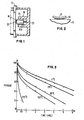
- FIG. 3 shows the relative relaxation times for a chip to be relieved of its stress as a function of temperature.
- the curves represent an initial strain of 2 percent and are plotted as the percentage of stress remaining versus time.
- the 25°C curve represents the closest approximation to room temperature, while the 85°C represents a temperature in excess of equipment ambient. It will be noted that at 25°C the chip will retain approximately 32% of its initial stress- after 6 hours. At 85°C the chip will exhibit about 18% of its initial stress after 5 hours. At 100°C the retained stress is approximately 17% after 4 hours. At 200°C, 20% of the stress remains after 1/2 hour.
- An integrated circuit module is an extremely complex assembly as will be evidenced from a study of one or more of the patents listed above. Therefore, the choice of parameters for relieving chip stress must take into account the effects of the heat treatment upon the total module assembly and all the materials therein. It is not a simple optimization of the process based on the characteristics of the solder alloy alone and reference to the phase diagram of the binary solder alloy used to connect the chips to the ceramic substrate.
- the cooling time required is a function of the temperature difference.
- the maximum time temperature product available for relaxing stresses in the chip-to-substrate interconnections is typically limited by degradation mechanisms in the interconnections and other metallurgical structures on a completed substrate chip carrier with attached integrated circuit chips.
- the continued formation of intermetallics with attendant Kirkendall void formation weakens these structures including, but not limited to, engineering change wires, pin braze connections, flange braze connections, and the interconnections between the integrated circuit chips and the substrate chip carrier.
- the foregoing parameters are typically achieved by using a box type furnace. To prevent oxidation of the solder pads, a reducing or inert atmosphere is required. The use of a nitrogen atmosphere is sufficient. Temperature has to be monitored. Since it is the chip to substrate interconnection which has to be at 200 0 C a control module having a precalibrated chip-to-substrate interconnection electrical resistance versus temperature is used to monitor the temperature.
- the first chip was reserved as a control to determine the effect, if any, of heat treatment only upon the device characteristics.
- the second and third chips were subjected to impact loading and then heat treated. Test data were.taken on the first chip before and after heat treatment. Data on the second and third chips were taken before loading, after loading, and after heat treatment.
- the effects are shown qualitatively and roughly quantitatively by the graphs of FIGS. 4A-4C.
- the coordinates of these curves are VEE for the horizontal axis and V BB for the vertical axis with the voltages increasing in the direction of the arrows.
- the curves themselves represent a constant response time of approximately 14.5 nanoseconds with the paired voltages indicated by the curves. Thus, the greater the area under the curve, the less is the energy required to produce the same response time in the device under test.
- FIG. 4A which represents the response of the control chip before and after heat treatment
- there is only one curve because the response of the device undergoes so insubstantial a change that the two curves (before and after heat treatment) are indistinguishable from one another. From this it can reasonably be concluded that heat treatment at 200 o C and 1/2 hour has no effect upon the device characteristics in an unstressed chip.
- the characteristics of the second chip, whose response was measured before impacting, after impacting, and after heat treatment are represented by the three curves a, b and c in FIG. 4B.
- Curve a represents the prestressed condition
- b the stressed condition
- c the post heat treatment condition.
- the b curve relative to the a and c curves manifests a substantial increase in the energy required to maintain a constant response.
- the substantial congruence of the a and c curves demonstrates the effectiveness of the heat treatment in restoring the device characteristics to the prestress values.
- FIG. 4C represents the characteristics of the third chip in the same manner as FIG. 4B does for chip No. 2. It provides further evidence of the adverse effect of impact-induced stress upon the device performance characteristics, and the restoration of those characteristics by the heat treatment.
Landscapes
- Wire Bonding (AREA)
- Electric Connection Of Electric Components To Printed Circuits (AREA)
- Heat Treatment Of Nonferrous Metals Or Alloys (AREA)
Applications Claiming Priority (2)
| Application Number | Priority Date | Filing Date | Title |
|---|---|---|---|
| US36945082A | 1982-04-19 | 1982-04-19 | |
| US369450 | 1989-06-21 |
Publications (3)
| Publication Number | Publication Date |
|---|---|
| EP0092041A2 true EP0092041A2 (de) | 1983-10-26 |
| EP0092041A3 EP0092041A3 (en) | 1986-04-16 |
| EP0092041B1 EP0092041B1 (de) | 1989-05-03 |
Family
ID=23455532
Family Applications (1)
| Application Number | Title | Priority Date | Filing Date |
|---|---|---|---|
| EP83101747A Expired EP0092041B1 (de) | 1982-04-19 | 1983-02-23 | Verfahren zur Spannungsentlastung in montierten Schaltungschips |
Country Status (3)
| Country | Link |
|---|---|
| EP (1) | EP0092041B1 (de) |
| JP (1) | JPS58191441A (de) |
| DE (1) | DE3379819D1 (de) |
Cited By (5)
| Publication number | Priority date | Publication date | Assignee | Title |
|---|---|---|---|---|
| EP0167030A1 (de) * | 1984-06-28 | 1986-01-08 | International Business Machines Corporation | Verfahren zur Bildung von Lötverbindungen für Halbleitervorrichtungen |
| FR2569052A1 (fr) * | 1984-08-10 | 1986-02-14 | Thomson Csf | Procede d'interconnexion de circuits integres |
| EP0977253A3 (de) * | 1998-05-06 | 2001-01-17 | Texas Instruments Incorporated | Flipchip-Verbindung von Halbleiterchips |
| CN104521334A (zh) * | 2012-08-06 | 2015-04-15 | 株式会社Kmw | 用于通过热沉耗散热量的设备 |
| CN111370318A (zh) * | 2018-12-25 | 2020-07-03 | 东莞新科技术研究开发有限公司 | 一种半导体消除内应力的方法 |
Family Cites Families (3)
| Publication number | Priority date | Publication date | Assignee | Title |
|---|---|---|---|---|
| US3486223A (en) * | 1967-04-27 | 1969-12-30 | Philco Ford Corp | Solder bonding |
| JPS5183164A (ja) * | 1975-01-07 | 1976-07-21 | Aimu Denki Kogyo Kk | Shuusekikairososhinodashinhizumitorisochi |
| US3993123A (en) * | 1975-10-28 | 1976-11-23 | International Business Machines Corporation | Gas encapsulated cooling module |
-
1983
- 1983-02-09 JP JP58019016A patent/JPS58191441A/ja active Pending
- 1983-02-23 DE DE8383101747T patent/DE3379819D1/de not_active Expired
- 1983-02-23 EP EP83101747A patent/EP0092041B1/de not_active Expired
Cited By (8)
| Publication number | Priority date | Publication date | Assignee | Title |
|---|---|---|---|---|
| EP0167030A1 (de) * | 1984-06-28 | 1986-01-08 | International Business Machines Corporation | Verfahren zur Bildung von Lötverbindungen für Halbleitervorrichtungen |
| US4611746A (en) * | 1984-06-28 | 1986-09-16 | International Business Machines Corporation | Process for forming improved solder connections for semiconductor devices with enhanced fatigue life |
| FR2569052A1 (fr) * | 1984-08-10 | 1986-02-14 | Thomson Csf | Procede d'interconnexion de circuits integres |
| EP0977253A3 (de) * | 1998-05-06 | 2001-01-17 | Texas Instruments Incorporated | Flipchip-Verbindung von Halbleiterchips |
| CN104521334A (zh) * | 2012-08-06 | 2015-04-15 | 株式会社Kmw | 用于通过热沉耗散热量的设备 |
| EP2882270A4 (de) * | 2012-08-06 | 2016-03-02 | Kmw Inc | Vorrichtung zur wärmeableitung durch einen kühlkörper |
| CN111370318A (zh) * | 2018-12-25 | 2020-07-03 | 东莞新科技术研究开发有限公司 | 一种半导体消除内应力的方法 |
| CN111370318B (zh) * | 2018-12-25 | 2024-04-09 | 东莞新科技术研究开发有限公司 | 一种半导体消除内应力的方法 |
Also Published As
| Publication number | Publication date |
|---|---|
| JPS58191441A (ja) | 1983-11-08 |
| DE3379819D1 (en) | 1989-06-08 |
| EP0092041B1 (de) | 1989-05-03 |
| EP0092041A3 (en) | 1986-04-16 |
Similar Documents
| Publication | Publication Date | Title |
|---|---|---|
| EP0550432B1 (de) | Elektrische Verbinderstruktur und Verfahren, einen elektrischen Verbindungsaufbau zu erhalten | |
| US5525545A (en) | Semiconductor chip assemblies and components with pressure contact | |
| CA1083261A (en) | Method for making conduction-cooled circuit package | |
| US5885849A (en) | Methods of making microelectronic assemblies | |
| EP0587337A1 (de) | Verfahren zum wiederentbindbaren metallischen Verbinden | |
| KR100760965B1 (ko) | 전자 부품 실장 방법 | |
| Clementi et al. | Flip-chip encapsulation on ceramic substrates | |
| EP0092041B1 (de) | Verfahren zur Spannungsentlastung in montierten Schaltungschips | |
| Fox et al. | Investigation of solder fatigue acceleration factors | |
| CN113070603A (zh) | 无铅无铜锡合金与用于球栅阵列封装的锡球 | |
| Darveaux et al. | Shear deformation of indium solder joints | |
| Sridhar et al. | Reliability study of doped lead free solder paste alloys by thermal cycling testing | |
| Vijayakumar et al. | The effect of iso-thermal aging on vibrational performance of SAC 105 and 305 alloys | |
| Clech et al. | Local CTE mismatch in SM leaded packages: a potential reliability concern | |
| US20030202332A1 (en) | Second level packaging interconnection method with improved thermal and reliability performance | |
| Lodge et al. | The impact of packaging on the reliability of flip-chip solder bonded devices | |
| KR19990037330A (ko) | 기억금속을 이용한 풀 웨이퍼 테스트 장치 | |
| JPS6114798A (ja) | はんだ相互接続を形成する方法 | |
| JP3014020B2 (ja) | 半導体装置の製造方法 | |
| JP3399418B2 (ja) | 表面実装型半導体装置の実装構造 | |
| Lee et al. | Computational model validation with experimental data from temperature cycling tests of PBGA assemblies for the analysis of board level solder joint reliability | |
| Xie et al. | Solder joint reliability of double-side mounted DDR modules for consumer and automotive applications | |
| Howell et al. | Area array solder interconnection technology for the three-dimensional silicon cube | |
| Wang et al. | Anisotropic conductive adhesives for flip-chip interconnects | |
| Wang et al. | Processing mechanics for flip-chip assembly |
Legal Events
| Date | Code | Title | Description |
|---|---|---|---|
| PUAI | Public reference made under article 153(3) epc to a published international application that has entered the european phase |
Free format text: ORIGINAL CODE: 0009012 |
|
| AK | Designated contracting states |
Designated state(s): DE FR GB |
|
| 17P | Request for examination filed |
Effective date: 19840218 |
|
| PUAL | Search report despatched |
Free format text: ORIGINAL CODE: 0009013 |
|
| AK | Designated contracting states |
Kind code of ref document: A3 Designated state(s): DE FR GB |
|
| 17Q | First examination report despatched |
Effective date: 19880701 |
|
| GRAA | (expected) grant |
Free format text: ORIGINAL CODE: 0009210 |
|
| AK | Designated contracting states |
Kind code of ref document: B1 Designated state(s): DE FR GB |
|
| REF | Corresponds to: |
Ref document number: 3379819 Country of ref document: DE Date of ref document: 19890608 |
|
| ET | Fr: translation filed | ||
| PLBE | No opposition filed within time limit |
Free format text: ORIGINAL CODE: 0009261 |
|
| STAA | Information on the status of an ep patent application or granted ep patent |
Free format text: STATUS: NO OPPOSITION FILED WITHIN TIME LIMIT |
|
| 26N | No opposition filed | ||
| PGFP | Annual fee paid to national office [announced via postgrant information from national office to epo] |
Ref country code: FR Payment date: 19950128 Year of fee payment: 13 |
|
| PGFP | Annual fee paid to national office [announced via postgrant information from national office to epo] |
Ref country code: DE Payment date: 19950223 Year of fee payment: 13 |
|
| PGFP | Annual fee paid to national office [announced via postgrant information from national office to epo] |
Ref country code: GB Payment date: 19960126 Year of fee payment: 14 |
|
| PG25 | Lapsed in a contracting state [announced via postgrant information from national office to epo] |
Ref country code: FR Effective date: 19961031 |
|
| PG25 | Lapsed in a contracting state [announced via postgrant information from national office to epo] |
Ref country code: DE Effective date: 19961101 |
|
| REG | Reference to a national code |
Ref country code: FR Ref legal event code: ST |
|
| PG25 | Lapsed in a contracting state [announced via postgrant information from national office to epo] |
Ref country code: GB Effective date: 19970223 |
|
| GBPC | Gb: european patent ceased through non-payment of renewal fee |
Effective date: 19970223 |