EP0087665B1 - Strain sensor - Google Patents
Strain sensor Download PDFInfo
- Publication number
- EP0087665B1 EP0087665B1 EP83101379A EP83101379A EP0087665B1 EP 0087665 B1 EP0087665 B1 EP 0087665B1 EP 83101379 A EP83101379 A EP 83101379A EP 83101379 A EP83101379 A EP 83101379A EP 0087665 B1 EP0087665 B1 EP 0087665B1
- Authority
- EP
- European Patent Office
- Prior art keywords
- load cell
- creep
- strain sensor
- powder
- insulating
- Prior art date
- Legal status (The legal status is an assumption and is not a legal conclusion. Google has not performed a legal analysis and makes no representation as to the accuracy of the status listed.)
- Expired
Links
Images


Classifications
-
- G—PHYSICS
- G01—MEASURING; TESTING
- G01L—MEASURING FORCE, STRESS, TORQUE, WORK, MECHANICAL POWER, MECHANICAL EFFICIENCY, OR FLUID PRESSURE
- G01L1/00—Measuring force or stress, in general
- G01L1/20—Measuring force or stress, in general by measuring variations in ohmic resistance of solid materials or of electrically-conductive fluids; by making use of electrokinetic cells, i.e. liquid-containing cells wherein an electrical potential is produced or varied upon the application of stress
- G01L1/22—Measuring force or stress, in general by measuring variations in ohmic resistance of solid materials or of electrically-conductive fluids; by making use of electrokinetic cells, i.e. liquid-containing cells wherein an electrical potential is produced or varied upon the application of stress using resistance strain gauges
- G01L1/2287—Measuring force or stress, in general by measuring variations in ohmic resistance of solid materials or of electrically-conductive fluids; by making use of electrokinetic cells, i.e. liquid-containing cells wherein an electrical potential is produced or varied upon the application of stress using resistance strain gauges constructional details of the strain gauges
-
- Y—GENERAL TAGGING OF NEW TECHNOLOGICAL DEVELOPMENTS; GENERAL TAGGING OF CROSS-SECTIONAL TECHNOLOGIES SPANNING OVER SEVERAL SECTIONS OF THE IPC; TECHNICAL SUBJECTS COVERED BY FORMER USPC CROSS-REFERENCE ART COLLECTIONS [XRACs] AND DIGESTS
- Y10—TECHNICAL SUBJECTS COVERED BY FORMER USPC
- Y10T—TECHNICAL SUBJECTS COVERED BY FORMER US CLASSIFICATION
- Y10T29/00—Metal working
- Y10T29/49—Method of mechanical manufacture
- Y10T29/49002—Electrical device making
- Y10T29/49082—Resistor making
- Y10T29/49103—Strain gauge making
Definitions
- the present invention relates to a strain sensor adapted for a load cell weighing instrument or the like.
- a strain sensor is known from the DE-A-1 648 788. This document discloses a strain gauge on a substrate consisting of epoxy modified resin. It is stated, that a content of preferably 30% by volume of quartz powder will improve the heat resistance of the resin. The resin surrounds the resistance elements of this strain gauge on all sides. The strain gauge will be sticked onto a measuring object by a special adhesive.
- a conventional load cell weighing instrument as disclosed in the US Patent 4 104 605 has a beam body including a strain generating section, an insulating film formed of an inorganic oxide such as a silicon dioxide (Si0 2 ), an aluminum trioxide (AI 2 0 3 ) or a tantalum pentaoxide (Ta 2 0 5 ) formed on the beam body, and thin film resistors formed to construct a strain gauge bridge circuit on the insulating film.
- a load is, for example, applied to one end of the beam body, a strain is produced at the strain generating section, and this strain is transmitted to the thin film resistors through the insulating film.
- the resistances of the thin film resistors are varied in accordance with the magnitude of the strain, with the result that an output voltage from the bridge circuit will alter. If a predetermined load remains applied to the beam body, the output voltage of the bridge circuit will vary with time, and a so- called “creep phenomenon" will occur.
- the creep phenomenon is influenced by the quality of the material, the thickness, and the pattern of the thin film resistor, the quality of the material and the shape of the beam body, the quality of the material of the insulating film, and so forth.
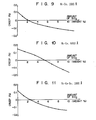
- Fig. 1 shows the creep characteristic of a conventional load cell which is constructed by forming a polyimide resin film of approx. 4 ⁇ m thickness on the beam body made of a stainless steel (SUS630), and forming thin film resistors of approx. 1000 A thickness.
- a rated load is applied to this load cell at a time t0, a rated output voltage VO substantially corresponding to this load is almost instantaneously produced from this load cell.
- the output voltage of this load cell gradually increases.
- the output voltage of this load cell for example, becomes (VO+AVO) at a time t1 after 10 minutes.
- the output voltage of the load cell When the load is removed from the load cell at this time t1, the output voltage of the load cell will instantaneously drop to AV1 having a value substantially equal to AVO. Thereafter, the output voltage of this load cell will gradually drop and will substantially return to OV at a time t2 after approx. 10 minutes has elapsed.
- Fig. 2 shows the creep characteristic of another conventional load cell which employs a silicon dioxide film (Si0 2 ) of 3 ⁇ m thickness instead of the polyimide resin film of 4 pm.
- the output voltage of this load cell drops to (VO-AV2) 10 minutes after the rated load is applied to the load cell.
- the output voltage from this load cell drops from (VO-AV2) to -AV3, and is then gradually raised to OV.
- the input voltage VI of a load cell having the creep characteristic shown in Fig. 1 is 10,000 mV
- the gauging factor K of the thin film resistors of this load cell is 1.8
- the output voltage VO of this load cell is given by the following equation:
- the creep of the load cell having the creep characteristic shown in Fig. 2 was: Even in this case, the accuracy of the load cell becomes lower than 1/1000, and again, an inaccurate load cell is provided.
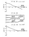
- the creep characteristic can be adjusted by varying the ratio of the effective length L of this thin film resistor R to the width I of the sides of the thin film resistor R in Fig. 3.
- the size of the resistor R is so determined as to reduce the ratio I/ L and in order to smoothen the curve of the creep characteristic shown in Fig. 2 that the size of the resistor R is so determined as to increase the ratio I/L.
- the creep cannot be reduced to substantially 0, that is, to such an extent the influence of the creeping phenomenon is negligible, and it is almost impossible to obtain a load cell of very high accuracy.
- a strain sensor which comprises an insulating film formed of an insulating resin and formed on the surface of a beam body having a strain generating section, and a resistance layer formed by deposition technique on the insulating resin film, whereby a solid powder is mixed at 2 to 20% by weight with said insulating resin film (4-1) and said solid powder is formed of at least one material selected from the group consisting of oxides, nitrides and sulfides.
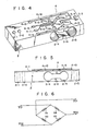
- Figs. 4 and 5 show perspective and side views of a load cell which is constructed with a strain sensor according to an embodiment of the present invention.
- This load cell has a beam body 2 which is obtained by cutting a stainless steel (SUS630) or duralumin (A2014, A2024 or A2218), and a load cell element or a strain sensor 4 formed on the beam body 2.
- This beam body 2 has two through holes 2-1 and 2-2 formed to receive clamping bolts at a stationary end, and a through hole 2-3 formed to receive a supporting clamp (not shown) for supporting a weighing tray at a movable end.
- this beam body 2 has two lateral through holes 2-4 and 2-5 formed to extend laterally, a coupling hole 2-6 for coupling the holes 2-4 and 2-5. Those portions of the beam body 2 corresponding to the top portions of the holes 2-4 and 2-5 form a strain generating section.
- the strain sensor 4 has a polyimide resin film 4-1 formed on the beam body 2 and having powder of silicon dioxide (Si0 2 ) mixed therein, four resistance elements 4-2 to 4-5 formed on the film 4-1 at a position corresponding to the strain generating section of the beam body 2, input terminals 4-6 and 4-7, output terminals 4-8 and 4-9, and conductive layers 4-10 which construct a strain gauge bridge circuit having an equivalent circuit shown in Fig. 6 by selectively coupling the four resistance elements 4-2 to 4-5, and the input and output terminals 4-6 to 4-9.
- resistors R1 to R4 correspond to the resistance elements 4-2 to 4-5, respectively, input terminals VI1 and VI2 respectively correspond to the input terminals 4-6 and 4-7, and output terminals V01 and V02 respectively correspond to the output terminals 4-8 and 4-9.
- a fine powder of the Si0 2 having, for example, a mean particle diametbr of 15 nm is first mixed with the varnish of the polyimide resin, is then uniformly diffused in the polyimide resin varnish, and a polyimide varnish having 1000 mPa.s of a viscosity is thus prepared.
- the surface of the beam body 2 which is obtained by cutting a stainless steel plate (SUS630) is degreased and cleaned, the polyimide varnish containing the Si0 2 powder having a viscosity of 1000 mPa.s is then dropped on the cleaned surface of the beam body 2, and the beam body 2 is rotated by a spinner at a rotating speed of 1500 r.p.m., thereby making the thickness of the polyimide varnish film uniform.
- the beam body 2 is heated at 350°C for approx. 1 hour to evaporate a solvent of the polyimide varnish, the polyimide resin is cured, and a polyimide resin film mixed with the fine powder of Si0 2 and having a thickness of approx. 4 ⁇ m is formed on the beam body 2.
- the above-mentioned heat treatment is effected under a temperature of 200°C instead of 350°C.
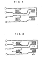
- a resistance layer of nickel-chrome [containing by weight percentage 50% of nickel (Ni) and 50% of chromium (Cr)] of 1000 ⁇ thickness is formed by sputtering on this polyimide resin film, and a gold (Au) layer having a thickness of 2 urn is formed by sputtering on the resistance layer.
- a laminate of this resistance layer and the gold layer is selectively etched out by a photoetching process to form a lamination of a predetermined pattern as shown in Fig. 7.
- the gold layer is selectively removed by etching, and selected portions of the resistance layer are exposed as shown by shaded parts in Fig. 8, thereby forming resistance elements 4-2 to 4-5.
- a plurality of load cell groups each including five load cells each of which was constructed in such a manner as described above, were prepared.
- the load cells in the same load cell group had the polyimide resin films mixed with the Si0 2 powder by the same weight percentage, and the Si0 2 powder is mixed in the polyimide resin film of each load cell of one load cell group by a weight percentage different from that by which the Si0 2 powder is mixed in the polyimide resin film of each load cell of another load cell group.
- the ratio (I/L) of the resistance elements 4-2 to 4-5 of each load cell was set to 1/20.
- the rated output voltages of these load cells were measured at a time of application of the rated load and at a time 10 min. after this rated load application time. Thus, five creep measurements were obtained for the same weight percentage of the Si0 2 powder.
- Fig. 9 shows the relationship between the creep (means value) of the same type load cell and the weight percentage of the Si0 2 powder.
- Fig. 10 shows the relationship between the weight percentage of the Si0 2 powder and the creep (mean value) of each load cell in which the film thicknesses of the resistance elements 4-2 to 4-5 are changed to 6000 A. Even in this case, as the weight percentage of the Si0 2 powder is increased, the creep decreases, and the creep becomes 0 when the weight percentage becomes approx. 5.3%. In other words, a load cell in which the creep becomes substantially zero can be obtained when the Si0 2 powder is mixed in the polyimide resin to an extent greater than the amount of the example in Fig. 9.
- Fig. 11 shows the relationship between the creep (mean value) of each load cell in which a resistance layer having a thickness of 1000 A is formed of nickel-chrome-silicon (containing 70% of Ni, 20% of Cr and 10% of Si by weight percentage) instead of the nickel-chrome and the weight percentage of the Si0 2 powder. Also in this case, as the weight percentage of the Si0 2 is increased, the creep decreases, and the creep becomes 0 when the weight percentage becomes approx. 2.5%.
- Fig. 12 shows the relationship between the weight percentage of the Si0 2 powder and the creep (mean value) of each load cell in which a resistance layer having a thickness of 6000 A is formed of nickel-chrome-silicon instead of the nickel-chrome.
- the creep becomes 0 when the weight percentage of the Si0 2 powder becomes around 6.8%.
- Figs. 14 to 17 each show the relationship between the weight percentage of the Si0 2 powder in the polyimide resin and the creep (means values) of each of the respective load cells in which the polyimide resin films 4-1 are formed with a thickness of 4 pm and the resistance layers are respectively formed of nickel-chrome of 1000 A thickness, nickel-chrome of 6000 A, nickel-chrome-silicon of 1000 A and nickei-chrome-siii- con of 6000 A.
- the Si0 2 powder should be mixed with the polyimide resin at a weight percentage larger than that of the examples shown in Figs. 9 to 12.
- the creep becomes substantially zero when 15%, 20%, 15% and 20% of the Si0 2 powders are respectively mixed with the polyimide resin in the examples shown in Figs. 14 to 17.
- the creep of the load cell can be suppressed to substantially zero by suitably selecting the weight percentage of the Si0 2 powder mixed with the polyimide resin film.
- the Si0 2 powder is used as the solid powder to be mixed with the insulating resin film 4-1.
- substances which are not chemically reacted with the insulating resin film for example, powders of aluminum trioxide (AI 2 0 3 ), magnesium oxide (MgO), titanium dioxide (Ti0 2 ), boron nitride (BN), or molybdenum sulfide (MoS 2 ) instead of the Si0 2 powder.
- these solid substances may be used in a mixture.
- a conductive powder such as carbon to such an extent that the insulating property of the insulating resin film will not be lost.
- the polyimide resin is employed as the insulating resin.
- another insulating resin if it exhibits a preferable adhesion to the resistance layer which forms the beam body 2 and the resistance elements 4-2 to 4-5.
- the insulating resin film 4-1 is slightly heated when the resistance layer is formed by sputtering or depositing process, it is necessary to incorporate a certain degree of heat resistance, for example, at least higher than 100°C. Insulating resins which can satisfy such conditions include, in addition to the polyimide resin, cyclic polybutadiene resin, epoxy resin, and epoxy modified polyimide resin.
- the insulating resin film be formed to a thickness greater than 1 pm so as to obtain preferable insulating properties between the resistance layer and the beam body, and that the resin film be formed to a thickness less than 20 ⁇ m so as to form the film uniformly on the beam body.
- the mean particle diameter of the Si0 2 powder is set to 15 nm.
- a solid powder having mean particle diameters of 7 nm to 40 nm such as is commonly sold as a thickening material for ordinary paint.
Applications Claiming Priority (2)
| Application Number | Priority Date | Filing Date | Title |
|---|---|---|---|
| JP57024939A JPS58142206A (ja) | 1982-02-18 | 1982-02-18 | 歪センサ |
| JP24939/82 | 1982-02-18 |
Publications (3)
| Publication Number | Publication Date |
|---|---|
| EP0087665A2 EP0087665A2 (en) | 1983-09-07 |
| EP0087665A3 EP0087665A3 (en) | 1983-10-19 |
| EP0087665B1 true EP0087665B1 (en) | 1987-11-19 |
Family
ID=12152018
Family Applications (1)
| Application Number | Title | Priority Date | Filing Date |
|---|---|---|---|
| EP83101379A Expired EP0087665B1 (en) | 1982-02-18 | 1983-02-14 | Strain sensor |
Country Status (7)
| Country | Link |
|---|---|
| US (1) | US4511877A (ja) |
| EP (1) | EP0087665B1 (ja) |
| JP (1) | JPS58142206A (ja) |
| KR (1) | KR860001781B1 (ja) |
| AU (1) | AU536998B2 (ja) |
| CA (1) | CA1184051A (ja) |
| DE (1) | DE3374602D1 (ja) |
Families Citing this family (31)
| Publication number | Priority date | Publication date | Assignee | Title |
|---|---|---|---|---|
| JPS59230131A (ja) * | 1983-06-13 | 1984-12-24 | Tokyo Electric Co Ltd | ロ−ドセル |
| DE3403042A1 (de) * | 1984-01-30 | 1985-08-01 | Philips Patentverwaltung Gmbh, 2000 Hamburg | Duennfilm-dehnungsmessstreifen-system und verfahren zu seiner herstellung |
| DE3579601D1 (de) * | 1984-01-28 | 1990-10-18 | Philips Patentverwaltung | Verfahren zur herstellung eines duennfilmmessstreifensystems. |
| DE3404936A1 (de) * | 1984-02-11 | 1985-08-14 | Bizerba-Werke Wilhelm Kraut GmbH & Co KG, 7460 Balingen | Elektromechanische waegezelle mit biegemesskoerper |
| EP0251563A3 (en) * | 1986-06-17 | 1991-01-09 | Tokyo Electric Co. Ltd. | Photoelectric conversion device |
| JPS63165725A (ja) * | 1986-12-26 | 1988-07-09 | Aisin Seiki Co Ltd | 圧力センサ−用歪ゲ−ジ |
| JPH0731091B2 (ja) * | 1987-05-27 | 1995-04-10 | 日本碍子株式会社 | 歪検出器 |
| US4821583A (en) * | 1987-07-14 | 1989-04-18 | E. I. Du Pont De Nemours And Company | Tension measuring apparatus |
| FR2622008B1 (fr) * | 1987-10-15 | 1990-01-19 | Commissariat Energie Atomique | Jauges de contrainte a fluage reglable et procede d'obtention de telles jauges |
| JPH01124731A (ja) * | 1988-10-05 | 1989-05-17 | Tokyo Electric Co Ltd | 歪センサ |
| US5184520A (en) * | 1989-10-18 | 1993-02-09 | Ishida Scales Mfg. Co., Ltd. | Load sensor |
| US5154247A (en) * | 1989-10-31 | 1992-10-13 | Teraoka Seiko Co., Limited | Load cell |
| US5306873A (en) * | 1990-09-26 | 1994-04-26 | Ishida Scales Mfg. Co., Ltd. | Load cell with strain gauges having low temperature dependent coefficient of resistance |
| DE59108247D1 (de) * | 1991-11-30 | 1996-11-07 | Endress Hauser Gmbh Co | Verfahren zum Stabilisieren der Oberflächeneigenschaften von in Vakuum temperaturzubehandelnden Gegenständen |
| FR2685080B1 (fr) * | 1991-12-17 | 1995-09-01 | Thomson Csf | Capteur mecanique comprenant un film de polymere. |
| FR2693795B1 (fr) * | 1992-07-15 | 1994-08-19 | Commissariat Energie Atomique | Jauge de contrainte sur support souple et capteur muni de ladite jauge. |
| JPH115364A (ja) * | 1997-04-24 | 1999-01-12 | Tec Corp | ノンインパクト記録方法 |
| JP3998046B2 (ja) * | 1997-08-22 | 2007-10-24 | 株式会社イシダ | ロードセルの製造方法およびロードセル |
| US6647797B2 (en) * | 1997-11-06 | 2003-11-18 | Powerco, S.P.A. | Strain gauge strip and applications thereof |
| DE19814261A1 (de) * | 1998-03-31 | 1999-10-14 | Mannesmann Vdo Ag | Dehnungsempfindlicher Widerstand |
| US6453748B1 (en) | 1999-12-15 | 2002-09-24 | Wayne State University | Boron nitride piezoresistive device |
| US6680668B2 (en) * | 2001-01-19 | 2004-01-20 | Vishay Intertechnology, Inc. | Fast heat rise resistor using resistive foil |
| DE10156160B4 (de) * | 2001-11-15 | 2007-06-14 | Siemens Ag | Mechanisch-elektrischer Wandler |
| AU2002228515A1 (en) * | 2002-01-13 | 2003-07-24 | Piotr Buczkowski | Method for measuring the pipeline creeping |
| FR2867275B1 (fr) | 2004-03-03 | 2006-05-19 | Seb Sa | Capteur de poids |
| US7231803B2 (en) * | 2004-06-11 | 2007-06-19 | Robert Bosch Gmbh | Hybrid impact sensor |
| US7188511B2 (en) * | 2004-06-11 | 2007-03-13 | Robert Bosch Gmbh | Stress wave sensor |
| ITTO20120293A1 (it) | 2012-04-03 | 2013-10-04 | Metallux Sa | Procedimento per tarare un elemento di calibrazione, e relativo dispositivo |
| JPWO2014188678A1 (ja) * | 2013-05-21 | 2017-02-23 | パナソニックIpマネジメント株式会社 | 荷重検出装置 |
| JP2017067764A (ja) * | 2015-09-29 | 2017-04-06 | ミネベアミツミ株式会社 | ひずみゲージ、荷重センサ、及びひずみゲージの製造方法 |
| CN115030942B (zh) * | 2022-06-08 | 2023-08-18 | 深圳市力合鑫源智能技术有限公司 | 导热膜基底金属电阻应变计及其制备方法 |
Citations (1)
| Publication number | Priority date | Publication date | Assignee | Title |
|---|---|---|---|---|
| US4104605A (en) * | 1976-09-15 | 1978-08-01 | General Electric Company | Thin film strain gauge and method of fabrication |
Family Cites Families (7)
| Publication number | Priority date | Publication date | Assignee | Title |
|---|---|---|---|---|
| CA689756A (en) * | 1964-06-30 | The Budd Company | Bending-strain transducer | |
| DE1648788A1 (de) * | 1968-01-05 | 1971-07-22 | Tech Physikalische Werkstaette | Dehnungsmessstreifen mit Traeger aus Kunststoff |
| US4050976A (en) * | 1976-01-27 | 1977-09-27 | Bofors America, Inc. | Strain gage application |
| DE2728916A1 (de) * | 1977-06-27 | 1979-01-18 | Hottinger Messtechnik Baldwin | Verfahren und vorrichtung zum abdecken eines dehnungsmesstreifens |
| DE2916427C2 (de) * | 1979-04-23 | 1987-02-12 | Hottinger Baldwin Messtechnik Gmbh, 6100 Darmstadt | Meßumformer mit einer Feder und einer darauf applizierten Dehnungsmeßstreifenanordnung |
| DE2916425C2 (de) * | 1979-04-23 | 1981-04-09 | Siemens AG, 1000 Berlin und 8000 München | Dehnungsmeßstreifen und Verfahren zu seiner Herstellung |
| DE3176209D1 (en) * | 1980-11-29 | 1987-06-25 | Tokyo Electric Co Ltd | Load cell and method of manufacturing the same |
-
1982
- 1982-02-18 JP JP57024939A patent/JPS58142206A/ja active Granted
-
1983
- 1983-02-09 US US06/465,344 patent/US4511877A/en not_active Expired - Lifetime
- 1983-02-10 AU AU11306/83A patent/AU536998B2/en not_active Ceased
- 1983-02-14 EP EP83101379A patent/EP0087665B1/en not_active Expired
- 1983-02-14 DE DE8383101379T patent/DE3374602D1/de not_active Expired
- 1983-02-15 KR KR1019830000611A patent/KR860001781B1/ko not_active IP Right Cessation
- 1983-02-16 CA CA000421674A patent/CA1184051A/en not_active Expired
Patent Citations (1)
| Publication number | Priority date | Publication date | Assignee | Title |
|---|---|---|---|---|
| US4104605A (en) * | 1976-09-15 | 1978-08-01 | General Electric Company | Thin film strain gauge and method of fabrication |
Also Published As
| Publication number | Publication date |
|---|---|
| JPS58142206A (ja) | 1983-08-24 |
| US4511877A (en) | 1985-04-16 |
| EP0087665A2 (en) | 1983-09-07 |
| JPH0371641B2 (ja) | 1991-11-14 |
| CA1184051A (en) | 1985-03-19 |
| AU536998B2 (en) | 1984-05-31 |
| EP0087665A3 (en) | 1983-10-19 |
| AU1130683A (en) | 1983-08-25 |
| KR840003838A (ko) | 1984-10-04 |
| KR860001781B1 (ko) | 1986-10-22 |
| DE3374602D1 (en) | 1987-12-23 |
Similar Documents
| Publication | Publication Date | Title |
|---|---|---|
| EP0087665B1 (en) | Strain sensor | |
| US4320655A (en) | Quantity of flow meter | |
| EP0657898B1 (en) | Electrical resistor | |
| EP0426442B1 (en) | Load cell | |
| DE69822770T2 (de) | Dickschicht-Piezoresistive-Fühleranordnung | |
| EP0065419B1 (en) | Strain gauge | |
| US4329878A (en) | Bridge circuit formed of two or more resistance strain gauges | |
| KR960013675B1 (ko) | 변형센서 및 그 제조방법과 그 변형센서를 사용한 로드셀 저울 | |
| EP0035351B1 (en) | Deformable flexure element for strain gage transducer and method of manufacture | |
| DE4324040B4 (de) | Massenstromsensor | |
| US4907341A (en) | Compound resistor manufacturing method | |
| EP1999445B1 (de) | Dehnungsmessstreifen und messgrössenaufnehmer mit mindestens einem dehnungsmessstreifen | |
| DE60025355T2 (de) | Dehnungsmessstreifen | |
| KR100535897B1 (ko) | 로드셀및그제조방법 | |
| DE4033133C2 (de) | Last-Meßfühler | |
| US4100524A (en) | Electrical transducer and method of making | |
| EP1422730A1 (en) | High precision power resistors | |
| DE3040448A1 (de) | Mengendurchflussmesser fuer fluessigkeiten | |
| JP2001110602A (ja) | 薄膜抵抗体形成方法及びセンサ | |
| JPS58118930A (ja) | ロ−ドセル | |
| JPH033882B2 (ja) | ||
| JPH0129249B2 (ja) | ||
| JPH0258304A (ja) | 薄膜白金温度センサ | |
| JPS5940103A (ja) | 歪センサ | |
| Grange et al. | Thin film strain gauges on polymers: main characteristics |
Legal Events
| Date | Code | Title | Description |
|---|---|---|---|
| PUAI | Public reference made under article 153(3) epc to a published international application that has entered the european phase |
Free format text: ORIGINAL CODE: 0009012 |
|
| PUAL | Search report despatched |
Free format text: ORIGINAL CODE: 0009013 |
|
| 17P | Request for examination filed |
Effective date: 19830307 |
|
| AK | Designated contracting states |
Designated state(s): DE FR GB IT NL |
|
| AK | Designated contracting states |
Designated state(s): DE FR GB IT NL |
|
| GRAA | (expected) grant |
Free format text: ORIGINAL CODE: 0009210 |
|
| AK | Designated contracting states |
Kind code of ref document: B1 Designated state(s): DE FR GB NL |
|
| REF | Corresponds to: |
Ref document number: 3374602 Country of ref document: DE Date of ref document: 19871223 |
|
| ET | Fr: translation filed | ||
| PLBE | No opposition filed within time limit |
Free format text: ORIGINAL CODE: 0009261 |
|
| STAA | Information on the status of an ep patent application or granted ep patent |
Free format text: STATUS: NO OPPOSITION FILED WITHIN TIME LIMIT |
|
| 26N | No opposition filed | ||
| PGFP | Annual fee paid to national office [announced via postgrant information from national office to epo] |
Ref country code: DE Payment date: 20010205 Year of fee payment: 19 |
|
| PGFP | Annual fee paid to national office [announced via postgrant information from national office to epo] |
Ref country code: FR Payment date: 20010213 Year of fee payment: 19 |
|
| PGFP | Annual fee paid to national office [announced via postgrant information from national office to epo] |
Ref country code: GB Payment date: 20010214 Year of fee payment: 19 |
|
| PGFP | Annual fee paid to national office [announced via postgrant information from national office to epo] |
Ref country code: NL Payment date: 20010228 Year of fee payment: 19 |
|
| REG | Reference to a national code |
Ref country code: GB Ref legal event code: IF02 |
|
| PG25 | Lapsed in a contracting state [announced via postgrant information from national office to epo] |
Ref country code: GB Free format text: LAPSE BECAUSE OF NON-PAYMENT OF DUE FEES Effective date: 20020214 |
|
| PG25 | Lapsed in a contracting state [announced via postgrant information from national office to epo] |
Ref country code: NL Free format text: LAPSE BECAUSE OF NON-PAYMENT OF DUE FEES Effective date: 20020901 |
|
| PG25 | Lapsed in a contracting state [announced via postgrant information from national office to epo] |
Ref country code: DE Free format text: LAPSE BECAUSE OF NON-PAYMENT OF DUE FEES Effective date: 20020903 |
|
| GBPC | Gb: european patent ceased through non-payment of renewal fee |
Effective date: 20020214 |
|
| PG25 | Lapsed in a contracting state [announced via postgrant information from national office to epo] |
Ref country code: FR Free format text: LAPSE BECAUSE OF NON-PAYMENT OF DUE FEES Effective date: 20021031 |
|
| NLV4 | Nl: lapsed or anulled due to non-payment of the annual fee |
Effective date: 20020901 |
|
| REG | Reference to a national code |
Ref country code: FR Ref legal event code: ST |