EP0081055B1 - Aufzeichnungsträger mit einer mehrfarbigen Feinstruktur, insbesondere in Form einer Mikrolandkarte, und Verfahren zur Herstellung des Aufzeichnungsträgers - Google Patents
Aufzeichnungsträger mit einer mehrfarbigen Feinstruktur, insbesondere in Form einer Mikrolandkarte, und Verfahren zur Herstellung des Aufzeichnungsträgers Download PDFInfo
- Publication number
- EP0081055B1 EP0081055B1 EP82109176A EP82109176A EP0081055B1 EP 0081055 B1 EP0081055 B1 EP 0081055B1 EP 82109176 A EP82109176 A EP 82109176A EP 82109176 A EP82109176 A EP 82109176A EP 0081055 B1 EP0081055 B1 EP 0081055B1
- Authority
- EP
- European Patent Office
- Prior art keywords
- layer
- layers
- recording medium
- absorption
- layered
- Prior art date
- Legal status (The legal status is an assumption and is not a legal conclusion. Google has not performed a legal analysis and makes no representation as to the accuracy of the status listed.)
- Expired
Links
Images


Classifications
-
- G—PHYSICS
- G03—PHOTOGRAPHY; CINEMATOGRAPHY; ANALOGOUS TECHNIQUES USING WAVES OTHER THAN OPTICAL WAVES; ELECTROGRAPHY; HOLOGRAPHY
- G03F—PHOTOMECHANICAL PRODUCTION OF TEXTURED OR PATTERNED SURFACES, e.g. FOR PRINTING, FOR PROCESSING OF SEMICONDUCTOR DEVICES; MATERIALS THEREFOR; ORIGINALS THEREFOR; APPARATUS SPECIALLY ADAPTED THEREFOR
- G03F7/00—Photomechanical, e.g. photolithographic, production of textured or patterned surfaces, e.g. printing surfaces; Materials therefor, e.g. comprising photoresists; Apparatus specially adapted therefor
- G03F7/004—Photosensitive materials
- G03F7/09—Photosensitive materials characterised by structural details, e.g. supports, auxiliary layers
- G03F7/095—Photosensitive materials characterised by structural details, e.g. supports, auxiliary layers having more than one photosensitive layer
-
- G—PHYSICS
- G03—PHOTOGRAPHY; CINEMATOGRAPHY; ANALOGOUS TECHNIQUES USING WAVES OTHER THAN OPTICAL WAVES; ELECTROGRAPHY; HOLOGRAPHY
- G03C—PHOTOSENSITIVE MATERIALS FOR PHOTOGRAPHIC PURPOSES; PHOTOGRAPHIC PROCESSES, e.g. CINE, X-RAY, COLOUR, STEREO-PHOTOGRAPHIC PROCESSES; AUXILIARY PROCESSES IN PHOTOGRAPHY
- G03C7/00—Multicolour photographic processes or agents therefor; Regeneration of such processing agents; Photosensitive materials for multicolour processes
-
- Y—GENERAL TAGGING OF NEW TECHNOLOGICAL DEVELOPMENTS; GENERAL TAGGING OF CROSS-SECTIONAL TECHNOLOGIES SPANNING OVER SEVERAL SECTIONS OF THE IPC; TECHNICAL SUBJECTS COVERED BY FORMER USPC CROSS-REFERENCE ART COLLECTIONS [XRACs] AND DIGESTS
- Y10—TECHNICAL SUBJECTS COVERED BY FORMER USPC
- Y10S—TECHNICAL SUBJECTS COVERED BY FORMER USPC CROSS-REFERENCE ART COLLECTIONS [XRACs] AND DIGESTS
- Y10S428/00—Stock material or miscellaneous articles
- Y10S428/913—Material designed to be responsive to temperature, light, moisture
-
- Y—GENERAL TAGGING OF NEW TECHNOLOGICAL DEVELOPMENTS; GENERAL TAGGING OF CROSS-SECTIONAL TECHNOLOGIES SPANNING OVER SEVERAL SECTIONS OF THE IPC; TECHNICAL SUBJECTS COVERED BY FORMER USPC CROSS-REFERENCE ART COLLECTIONS [XRACs] AND DIGESTS
- Y10—TECHNICAL SUBJECTS COVERED BY FORMER USPC
- Y10T—TECHNICAL SUBJECTS COVERED BY FORMER US CLASSIFICATION
- Y10T428/00—Stock material or miscellaneous articles
- Y10T428/24—Structurally defined web or sheet [e.g., overall dimension, etc.]
- Y10T428/24802—Discontinuous or differential coating, impregnation or bond [e.g., artwork, printing, retouched photograph, etc.]
- Y10T428/24917—Discontinuous or differential coating, impregnation or bond [e.g., artwork, printing, retouched photograph, etc.] including metal layer
Definitions
- the invention relates to a recording medium with a multi-colored fine structure.
- US Pat. No. 3,727,233 describes a method for recording a multicolored image in which a metal layer of high reflectivity and an organic polymer layer are applied to a layer support made of glass.
- the polymer layer is exposed by means of electron beams penetrating an object to be imaged and then developed and then has a structure corresponding to the radiation intensity of the electron beams by means of polymerization.
- a further metal layer of high reflectivity is then applied to the structured organic polymer layer, so that a multicolored image results in natural light as a result of interference. It proves to be disadvantageous that the metal layers applied over the entire layer support with the same layer thickness do not allow different saturations of the individual color tones of the image.
- the structured interference layer in the form of the organic polymer layer because of its considerable sensitivity to heat, does not allow the multicolored image to be greatly re-enlarged due to the associated high illuminance levels; Due to the lack of lightfastness and shrinkage of the organic interference layer over time, color changes can also occur.
- DE-A No. 2658623 discloses a recording medium with a recording of high information density, in particular with a multicolored microimage, in which at least two interference filters for two different color tones are provided on a layer carrier.
- Each interference filter consists of an unstructured inorganic absorption-free interference layer which extends with the same layer thickness over the entire layer support and is delimited on each side by at least one inorganic reflective layer which forms the structure of the recording.
- the unstructured interference layer is delimited on each side by at least one structured highly refractive absorption-free layer, an unstructured low refractive absorption-free layer being located between every two high refractive layers.
- the unstructured interference layer is between the reflecting layers forming the structure and the unstructured interference layer and the unstructured low-refractive layers between the high-refractive layers forming the structure, which also extend with the same layer thickness over the entire layer support, there are a number of for each color Structuring steps are required, but in which the multiple adjustment of the exposure mask in question requires the greatest adjustment accuracy and is also time-consuming.
- the invention is based on the object of reducing the number of method steps in a recording medium of the type mentioned above, avoiding adjustment problems and improving the optical quality of the fine structure.
- this object is essentially achieved by the characterizing features of claim 1.
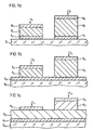
- 1 to 1 show recording media with metal-dielectric interference filters in the form of layer packets 11, 12, 13 for a first color and layer packs 2 1 , 2 2 , 2 3 for a second color.
- FIG. 1 For generating the first hue A is shown in FIG. 1 blanket deposited on a substrate 3 1 in a manner not shown, a first layer of photoresist and exposed using a first exposure mask. After the development of the first photoresist layer, a metal layer 4 1 , an inorganic absorption-free interference layer 5 1 according to the first color and a metal layer 6 are applied over the entire surface of the layer carrier 3 1 . The remaining first photoresist layer together with the layers 4 1 -6 1 located above it is then removed so that the layer package 1 1 remains on the layer support 3. To produce the second color tone, a second photoresist layer is applied over the entire surface of the layer support 3 and exposed using a second exposure mask.
- a metal layer 7 1 After the development of the second photoresist layer, a metal layer 7 1 , an inorganic absorption-free interference layer 8, according to the second color tone, and a metal layer 9 1 are applied over the entire surface of the layer support 3. The remaining second photoresist layer together with the overlying layers 7 1 -9 1 is then removed, so that remains next to the layer packet 1, layer 2 packet 1 on the substrate 3. 1
- this record carrier according to Fig. 1 b on a Layer support 3 2 has a metal layer 4 2 over its entire surface and a first photoresist layer is applied over it to produce the first color.
- a first photoresist layer is applied over it to produce the first color.
- an inorganic absorption-free interference layer 5 2 according to the first color and a metal layer 6 2 are applied over the entire surface of the metal layer 4 2 .
- the remaining first photoresist layer together with the overlying layers 5 2, 6 2 is then removed, so that the package of layers 1 2 remains on the substrate 3.
- a second photoresist layer is applied over the entire surface of the metal layer 4 2 and exposed using the second exposure mask.
- an inorganic absorption-free interference layer 8 2 according to the second color and a metal layer 9 2 are applied over the entire surface of the metal layer 4 2 .
- the remaining second photoresist layer together with the overlying layers 8 2, 9 2 is then removed, so that next to the layer 2, the package 1 layer packet 2 2 remains on the substrate 3.
- a metal layer 4 3 is applied over the entire surface of a layer support 3 3 and an inorganic absorption-free interference layer 5 3 is applied over it to produce the first color, which is subsequently covered over the entire surface with a first photoresist layer.
- a metal layer 6 3 on the substrate 3. 3 The remaining first photoresist layer together with the overlying metal layer 6 3 is then removed, so that the layer 3 packet 1 on the substrate 3 3 remains.
- a second photoresist layer is applied to the entire surface of the layer support 3 3 and exposed by means of the second exposure mask. After the development of the second photoresist layer, an inorganic absorption-free interference layer 8 3 and a metal layer 9 3 are applied over the entire surface of the layer carrier 3 3 . The remaining second photoresist layer together with the overlying layers 8 3 9 3 is then removed, so that next to the layer 3 packet 1, the layer 2 packet 3 remains on the substrate 3.
- the interference layers 5 3 , 8 3 together form the interference layer for the second color tone.
- the layers 4 1 , 5 1 , 6 1 in the case of the layer package 1 2, the layers 5 2 , 6 2 , in the case of the layer package 1 3, the layer 6 3 , in the case of the layer package 2 1, the layers 7 1 , 8 1 , 9 1 , in the case of the layer package 2 2, the layers 8 2 , 9 2 and in the case of the layer package 2 3, the layers 8 3 , 9 3 in each case the structure-forming part.
- the metal layers 4, 6, 7, 9 are partially permeable layers.
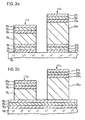
- 2a, 2b show recording media with pure dielectric interference filters in the form of layer packets 11 1 , 11 2 for a first color and layer packs 12 1 , 12 2 for a second color.
- a first photoresist layer is applied over the entire surface of a layer support 13 1 in a manner not shown in accordance with FIG. 2a and exposed using a first exposure mask.
- a highly refractive absorption-free layer 14 1 After the development of the first photoresist layer, a highly refractive absorption-free layer 14 1 , a low refractive absorption-free layer 15 1 , a highly refractive absorption-free layer 16 1 , an inorganic absorption-free interference layer 17 1 according to the first color, and a highly refractive absorption-free layer 18 are formed over the entire surface of the layer support 13 1 1 , a low-refraction absorption-free layer 19 1 and a high-refraction absorption-free layer 20 1 are applied.
- the remaining first photoresist layer together with the overlying layers 14 1 - 20 1 is then removed, so that the layer package 11 1 on the substrate 13 1 remains.
- a second photoresist layer is applied over the entire surface of the layer support 13 1 and exposed by means of a second exposure mask.
- a highly refractive absorption-free layer 21 1 , a low refractive absorption-free layer 22 1 , a highly refractive absorption-free layer 23 1 , an inorganic absorption-free interference layer 24 1 according to the second color, and a highly refractive absorption-free layer 25 are formed over the entire surface of the layer support 13 1 1 , a low-refraction absorption-free layer 26 1 and a high-refraction absorption-free layer 27 1 are applied.
- the remaining second photoresist layer together with the overlying layers 21 1 -27 1 is then removed, so that next to the layer 11 packet 1, the packet layer 12 1 remains on the substrate 13.
- a high-refractive absorption-free layer 14 2 , a low-refractive absorption-free layer 15 2 and a highly refractive absorption-free layer 16 2 are applied over the entire surface of a layer support 13 2, and a first photoresist layer is applied over it to produce the first color.
- a first photoresist layer is applied over it to produce the first color.
- an inorganic absorption-free interference layer 17 2 according to the first color, a highly refractive absorption-free layer 18 2 , a low-refraction absorption-free layer 19 2 and a high-refraction layer are applied over the entire surface of the layer 16 2 absorption-free layer 20 2 applied.
- the remaining first photoresist layer together with the overlying layers 17 2 -20 2 is then removed, so that the layer 2 remains package 11 on the substrate 13.
- 2 In order to produce the second color tone, 2 is entirely on layer 16 a second photoresist layer is applied to the surface and exposed by means of the second exposure mask. After the development of the second photoresist layer, an interference layer 24 2 in accordance with the second color tone, a high-refractive absorption-free layer 25 2 , a low-refractive absorption-free layer 26 2 and a highly refractive absorption-free layer 27 2 are applied over the entire surface of the layer 16 2 . The remaining second photoresist layer together with the above bedindlichen layers 24 2-27 2 is then removed, so that next to the layer package 11 2, the layer package 12 2 remains on the substrate 13. 2
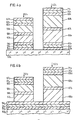
- 3a, 3b show recording media with half filters in the form of layer packets 31 1 , 31 2 for a first color and layer packs 32 1 , 32 2 for a second color.
- the layer package 31 1 on a layer support 33 1 consists of a high-index absorption-free layer 34 1 , a low-index absorption-free layer 35 1 , a high-index absorption-free layer 36 1 , an inorganic absorption-free interference layer 37 1 according to the first color and a metal layer 38 1 ; the layers 34 1 -38 1 form the structure-forming part of the layer package 31 1 .
- the layer package 32 1 on the layer support 33 1 consists of a highly refractive absorption-free layer 39 1 , a low refractive absorption-free layer 40 1 , a highly refractive absorption-free layer 41 1 , an inorganic absorption-free interference layer 42 1 according to the second color and a metal layer 43 1 ; the layers 39 1 -43 1 form the structure-forming part of the layer package 32 1 .
- the layer package 31 on a layer support 33 2 consists of a full-area, highly refractive absorption-free layer 34 2 , a full-area, low-refraction absorption-free layer 35 2 , a highly refractive absorption-free layer 36 2 , an inorganic absorption-free interference layer 37 2 according to the first color and a metal layer 38 2 ; the layers 36 2 -38 2 form the structure-forming part of the layer package 31 2 , while the entire surface layers 34 2 , 35 2 do not contribute to the structure formation.
- the layer package 32 2 on the layer support 33 2 consists of the full-area high-refraction absorption-free layer 34 2 , the full-area low-refraction absorption-free layer 35 2 , a high-refraction absorption-free layer 41z, an inorganic absorption-free interference layer 42 2 according to the second color and a metal layer 43 2 ; the layers 41 2 -43 2 form the structure-forming part of the layer package 32 2 , while the entire surface layers 34 2 , 352 do not contribute to the structure formation.
- 3a, 3b are produced in a photolithographic manner in the manner described above.
- the metal layers 38, 43 are partially permeable layers.
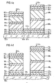
- the layer package 51 1 on a layer support 53 1 consists of a highly refractive absorption-free layer 54 1 , a low refractive absorption-free layer 55 1 , a highly refractive absorption-free layer 56 1 , a first inorganic absorption-free interference layer 57 1 according to the first color, a metal layer 58 1 , one second inorganic absorption-free interference layer 59 1 according to the first color, a high-index absorption-free layer 60 1 , a low-index absorption-free layer 61 1 and a high-index absorption-free layer 62 1 ; the layers 54 1 -62 1 form the structure-forming part of the layer package 51 1 .
- the layer package 52 1 on the layer support 53 1 consists of a high-index absorption-free layer 63 1 , a low-index absorption-free layer 64 1 , a high-index absorption-free layer 65 1 , a first inorganic absorption-free interference layer 66 1 according to the second color, a metal layer 67 1 , one second inorganic absorption-free interference layer 68 1 according to the second color, a high-refraction absorption-free layer 69 1 , a low-refraction absorption-free layer 70 1 and a high-refraction absorption-free layer 71 1 ; the layers 63 1 -71 1 form the structure-forming part of the layer package 52 1 .
- the layer package 51 2 on a layer support 53 2 consists of a full-area, high-index, absorption-free layer 54 2 , a full-area, low-index, absorption-free layer 55 2 , a full-area, high-index, absorption-free layer 56 2 , a first inorganic absorption-free interference layer 57 2 according to the first color, a metal layer 58 2 , a second inorganic absorption-free interference layer 59 2 according to the first color, a high-refraction absorption-free layer 60 2 , a low-refraction absorption-free layer 61 2 and a high-refraction absorption-free layer 62 2 ; the layers 57 2 -62 2 form the structure-forming part of the layer package 51 2 , while the entire surface layers 54 2 -56 2 do not contribute to the structure formation.
- the layer package 52 2 on the layer support 53 2 consists of the full-area, high-index, absorption-free layer 54 2 , the all-over, low-index, absorption-free layer 55 2 , the all-over, high-index, absorption-free layer 56 2 , a first inorganic absorption-free interference layer 66 2 according to the second color, a metal layer 67 2 , a second inorganic absorption-free interference layer 68 2 in accordance with the second color tone, a high width the absorption-free layer 69 2 , a low-refraction absorption-free layer 70 2 and a high-refraction absorption-free layer 71 2 ; the layers 66 2 -71 2 form the structure-forming part of the layer package 52 2 , while the entire surface layers 54 2 -56 2 do not contribute to the structure formation.
- 4a, 4b are produced by the photolithographic method in the manner described above.
- a first photoresist layer is applied over the entire surface in a manner not shown in FIG. 4c to produce the first color tone on a layer carrier 53 3 and is exposed by means of the first exposure mask.
- a high refractive absorption-free layer 54 3 After Entwikkein the first photoresist layer on the substrate 53 3 over the entire surface, a high refractive absorption-free layer 54 3, a low refractive absorption-free layer 55 3, a high-refraction absorption-free layer 56 3, a first inorganic absorption-free interference layer 57 3 according to the first hue, a layer of metal 58 3 and a second inorganic absorption-free interference layer 59 3 is applied in accordance with the first color tone.
- the remaining first photoresist layer together with the layers 54 3 -59 3 above it is then removed.
- a second photo is taken over the entire surface of the layer support 53 3 . lacquer layer applied and exposed by means of the second exposure mask.
- a high refractive absorption-free layer 63 3 a low refractive absorption-free layer 64 3
- a high-refraction absorption-free layer 65 a first inorganic absorption-free interference layer 66 3 according to the second hue
- a layer of metal 67 3 and a second inorganic absorption-free interference layer 68 3 is applied in accordance with the second color tone.
- the remaining second photoresist layer together with the layers 63 3 -68 3 above it is then removed.
- the structure-forming layers 54 3 -59 3 of the layer package 51 3 for the first color and the structure-forming layers 63 3 -68 3 of the layer package 52 3 for the second color are thus located on the layer support 53 3 .
- a high-refractive absorption-free layer 60 3 , a low-refractive absorption-free layer 61 3 and a high-refractive absorption-free layer 62 3 are then applied over the entire surface of the layer support 53 3 .
- the entire surface layers 60 3 -62 3 do not contribute to the structure formation.
- a first photoresist layer is applied over the entire surface in a manner not shown in FIG. 4d to produce the first color tone on a layer carrier 53 4 and is exposed by means of the first exposure mask.
- a high refractive absorption-free layer 54 4, a low-refraction absorption-free layer 55 4, a high refractive absorption-free layer 56 4 and a first inorganic absorption-free interference layer 57 4 are applied according to the first color over the entire surface on the substrate 53. 4
- the remaining first photoresist layer together with the layers 54 4 -57 4 located above it is then removed.
- a second photoresist layer is applied over the entire surface of the layer support 53 4 and exposed using the second exposure mask.
- the second photoresist layer After developing the second photoresist layer has a high index of refraction absorption-free layer 63 4, a low-refraction absorption-free layer 64 4, a high refractive absorption-free layer 65 4 and a first inorganic absorption-free interference layer 66 4 are applied according to the second color over the entire surface on the substrate 53. 4
- the remaining second photoresist layer together with the layers 63 4 -66 4 located above it is then removed.
- the first part of the structure-forming layers 54 4 -57 4 of the layer package 51 4 for the first color and the first part of the structure-forming layers 63 4 -66 4 of the layer package 52 4 for the second color are thus located on the layer support 53 4 .
- a metal layer 58 4 which does not contribute to pattern formation, and also for generating the first hue, a third Pho t olack Anlagen applied, which is exposed by the first exposure mask.
- a second inorganic absorption-free interference layer 59 4 according to the first color, a high-index absorption-free layer 60 4 , a low-index absorption-free layer 61 4 and a high-index absorption-free layer 62 4 are applied over the entire surface of the metal layer 58 4 .
- the remaining third photoresist layer together with the layers 59 4 -62 4 above it is then removed.
- a fourth photoresist layer is then applied over the entire surface of the metal layer 58 4 and exposed using the second exposure mask.
- a second inorganic absorption-free interference layer 68 4 according to the second color, a high-index absorption-free layer 69 4 , a low-index absorption-free layer 70 4 and a high-index absorption-free layer 71 4 are applied over the entire surface of the metal layer 58 4 .
- the remaining fourth photoresist layer together with the layers 68 4 -71 4 above it is then removed.
- the second part of the structure-forming layers 59 4 -62 4 of the layer package 51 4 for the first color and the second part of the structure-forming layers 68 4 -71 4 of the layer package 52 4 for the second color are thus located on the metal layer 58 4 .
- the metal layers 58, 67 are partially permeable layers.
- 5a, 5b are recording media with edge filters in the form of layer packets 81 1 , 81 2 for a first color and layer packets 82 1 , 82 2 shown for a second hue.
- the layer package 81 on a layer carrier 83 1 according to FIG. 5a, consists of two superimposed edge filters 84 1 -88 1 ; 89 1 -93 1 , which consists of highly refractive absorption-free layers 84 1 , 86 1 , 88 1 ; 89 1 , 91 1 , 93, exist between which low-refractive absorption-free layers 85 1 , 87 1 ; 90 1 , 92 1 .
- the layer package 82 1 on the layer carrier 83 consists of two edge filters 94 1 -98 1 lying one above the other; 99 1 -103 1 , which consists of highly refractive absorption-free layers 94 1 , 96 1 , 98 1 ; 99 1 , 101 1 , 103 1 exist between which low-refractive absorption-free layers 95 1 , 97 1 ; 100 1 , 102 1 .
- the layers 84 1 -93 1 of the two edge filters 84 1 -88 1 ; 89 1 -93 1 form the structure-forming part of the layer package 81 1 and the layers 94 1 -103 1 of the two edge filters 94 1 -98 1 ; 99 1 -103 1 the structure-forming part of the layer package 82 1 .
- the layer package 81 2 on a layer carrier 83 2 according to FIG. 5b consists of two edge filters 84 2 -88 2 lying one above the other; 89 2 -93 2 , of which the edge filter 84 2 -88 2 consists of full-area high-refraction absorption-free layers 84 2 , 862, 882, between which there are full-area low-refraction absorption-free layers 85 2 , 87 2 , and the edge filter 89 2 -93 2 high refractive absorption-free layers 89 2 , 91 2 , 93 2 exist, between which there are low refractive absorption free layers 90 2 , 92 2 ; the edge filter 90 2 -93 2 forms the structure-forming part of the layer package 81 2 .
- the layer package 82 2 on the layer carrier 83 2 consists of the full-surface edge filter 84 2 -88 2 , above which there is an edge filter 99 2 -103 2 , which consists of highly refractive absorption-free layers 99 2 , 101 2 , 103 2 , between which there is low-refraction absorption-free layers 100 2 , 102 2 are located.
- the edge filter 99 2 -103 2 forms the structure-forming part of the layer package 82 2 ; the all-over edge filter 84 2 -88 2 does not contribute to the structure formation of the layer packets 81 2 , 82 2 .
- Filters 1, 2; 11, 12; 31, 32; 51, 52, the first and second colors are determined by the optical thicknesses of the interference layers 5, 8; 17, 24; 37.42; 57, 59, 66, 68 and the saturation of these shades by the reflectivity of the metal layers 4, 6, 7, 9; 38, 43; 58, 67 or the high refractive index layers 14, 16, 18, 20, 21, 23, 25, 27; 34, 36, 39, 41; 54, 56, 60, 62, 63, 65, 69, 71 and the low refractive index layers 15, 19, 22, 26; 35, 40; 55, 61, 64, 70 determined.
- the spectral range of high transmission drops over a steep flank to a spectral range of low transmission.
- the optical layer thicknesses of the high-index and low-index layers of an edge filter are ⁇ / 4, where ⁇ means the greatest wavelength of the lowest transmission of the edge filter.
- Layer packets of this type can also be made from a combination of filters 1, 2; 11, 12; 31, 32; 51, 52; 81, 82 exist.
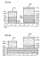
- 6a, 6b show recording media with edge filters and superimposed metal-dielectric interference filters in the form of layer packets 111 1 , 111 2 for a first color and of layer packs 112 1 , 112 2 for a second color.
- 6a consists of an edge filter 114 1 -118 1 with highly refractive absorption-free layers 114 1 , 116 1 , 118 1 , between which there are low-refraction absorption-free layers 115 1 , 117 1 , and from a metal-dielectric interference filter 119 1 -121 1 with an interference layer 120 1 , which is delimited on both sides by inorganic reflective layers 119 1 , 1211.
- the layer package 112 1 on the layer support 113 1 consists of an edge filter 122 1 -128 1 with highly refractive absorption-free layers 122 1 , 124 1 , 126 1 , 128 1 , between which there are low-refraction absorption layers 123 1 , 125 1 , 127 1 , and from a metal-dielectric interference filter 129 1 -131 1 with an interference layer 130 1 , which is delimited on both sides by inorganic reflective layers 129 1 , 131 1 .
- the layers 114 1 -121 1 form the structure-forming portion of the package layer 111 1 and the layers 122 1 -131 1 the structure-forming part of the layer package 112. 1
- the layer package 111 2 on a layer support 113 2 according to FIG. 6b consists of an edge filter 114 2 -118 2 with all-over high-refractive absorption-free layers 114 2 , 116 2 , 118 2 , between which there are all-over low-refraction absorption-free layers 115 2 , 117 2 , and from a metal-dielectric interference filter 119 2 -121 2 with an interference layer 120 2 , which is delimited on both sides by inorganic reflective layers 119 2 -121 2 is; the metal-dielectric interference filter 119 2 -121 2 forms the structure-forming part of the layer package 111 2 .
- the layer package 112 2 on the layer support 113 2 consists of the entire surface layers 114 2 -118 2 , of a low-refraction absorption-free layer 127 2 , of a high-refraction absorption-free layer 128 2 and of a metal-dielectric interference filter 129 2 -131 2 with an interference layer 130 2 , which is delimited on both sides by inorganic reflective layers 129 2 , 131 2 ; the layers 127z, 128 2 and the metal-dielectric interference filter 129 2 -131 2 form the structure-forming part of the layer package 112 2 .
- the inorganic reflective layers 4, 6, 7, 9; 38, 43; 58, 67; 119,121,129,131 consist of Ag, Cr, Au, Al or a combination of these materials, the interference layers 5, 8; 17, 24; 37, 42; 57, 59, 66, 68; 120, 130 made of MgF 2 , Si0 2 , Al 2 O 3 .
- the layer support 3; 13; 33; 53; 83; 113 can be made of transparent material or of
- the layer packages 1, 2; 11, 12; 31, 32; 51, 52; 81, 82; 111, 112 and / or structure-forming parts of these layer packages 1, 2; 11, 12; 31, 32; 51, 52; 81, 82; 111, 112 are preferably photolithographically one after the other - in the order of the shades of the fine structure - locally separated from each other on the layer support 3; 13; 33; 53; 83; 113 applied.
- the layer packs and / or the structure-forming parts of these layer packs can be produced on the layer support in a photolithographic way by means of wet chemical etching processes or physical etching processes such as ion beam etching, sputter etching, plasma etching or reactive ion etching.
- the layer packs and / or the structure-forming parts of these layer packs can each be produced by means of an evaporation mask or by means of a controlled particle beam (electron beam, ion beam, etc.).
- Layer packs with partially full-area layers can be produced on one layer support and layer packs without full-area layers on another part - also with different manufacturing processes.
- a border area is defined between adjacent different layer packets that have been generated one after the other, which represents a local separation of these layer packets.
- the application of the layers of the layer packages 1, 2; 11, 12; 31, 32; 51, 52; 81, 82; 111, 112 can be carried out, for example, by vapor deposition, sputtering, ion plating and separation from the vapor phase.
- the recording media according to the invention have in particular the advantage of improved color purity and color saturation and a reduction in rejects.
- the proposed recording medium is preferably used for recording multi-colored micro-maps.
Landscapes
- Physics & Mathematics (AREA)
- General Physics & Mathematics (AREA)
- Engineering & Computer Science (AREA)
- Architecture (AREA)
- Structural Engineering (AREA)
- Optical Filters (AREA)
- Optical Record Carriers And Manufacture Thereof (AREA)
- Non-Silver Salt Photosensitive Materials And Non-Silver Salt Photography (AREA)
- Instructional Devices (AREA)
- Developing Agents For Electrophotography (AREA)
- Manufacturing Optical Record Carriers (AREA)
- Paper (AREA)
- Laminated Bodies (AREA)
- Credit Cards Or The Like (AREA)
Priority Applications (1)
| Application Number | Priority Date | Filing Date | Title |
|---|---|---|---|
| AT82109176T ATE14484T1 (de) | 1981-12-04 | 1982-10-05 | Aufzeichnungstraeger mit einer mehrfarbigen feinstruktur, insbesondere in form einer mikrolandkarte, und verfahren zur herstellung des aufzeichnungstraegers. |
Applications Claiming Priority (2)
| Application Number | Priority Date | Filing Date | Title |
|---|---|---|---|
| DE3147985 | 1981-12-04 | ||
| DE3147985A DE3147985C2 (de) | 1981-12-04 | 1981-12-04 | Verfahren zur Herstellung eines Aufzeichnungsträgers mit einer mehrfarbigen Feinstruktur |
Publications (2)
| Publication Number | Publication Date |
|---|---|
| EP0081055A1 EP0081055A1 (de) | 1983-06-15 |
| EP0081055B1 true EP0081055B1 (de) | 1985-07-24 |
Family
ID=6147857
Family Applications (1)
| Application Number | Title | Priority Date | Filing Date |
|---|---|---|---|
| EP82109176A Expired EP0081055B1 (de) | 1981-12-04 | 1982-10-05 | Aufzeichnungsträger mit einer mehrfarbigen Feinstruktur, insbesondere in Form einer Mikrolandkarte, und Verfahren zur Herstellung des Aufzeichnungsträgers |
Country Status (8)
| Country | Link |
|---|---|
| US (1) | US4522862A (enExample) |
| EP (1) | EP0081055B1 (enExample) |
| JP (1) | JPS58144804A (enExample) |
| AT (1) | ATE14484T1 (enExample) |
| BR (1) | BR8207025A (enExample) |
| DE (1) | DE3147985C2 (enExample) |
| IL (1) | IL67365A (enExample) |
| ZA (1) | ZA828896B (enExample) |
Families Citing this family (13)
| Publication number | Priority date | Publication date | Assignee | Title |
|---|---|---|---|---|
| JPS60186804A (ja) * | 1984-03-06 | 1985-09-24 | Hisanori Bando | 光記録媒体 |
| JPH0672298B2 (ja) * | 1984-03-09 | 1994-09-14 | 京都大学 | 周期性を有する酸化物多層膜 |
| JPH0797216B2 (ja) * | 1986-10-29 | 1995-10-18 | インタ−ナショナル・ビジネス・マシ−ンズ・コ−ポレ−ション | マスクの製造方法 |
| US4923772A (en) * | 1986-10-29 | 1990-05-08 | Kirch Steven J | High energy laser mask and method of making same |
| US4713315A (en) * | 1986-12-09 | 1987-12-15 | Smith David V | Wire tag etching system |
| US4979803A (en) * | 1989-02-02 | 1990-12-25 | Eastman Kodak Company | Color filter array for area image sensors |
| US4956555A (en) * | 1989-06-30 | 1990-09-11 | Rockwell International Corporation | Multicolor focal plane arrays |
| JP2599513B2 (ja) * | 1990-06-25 | 1997-04-09 | インターナショナル・ビジネス・マシーンズ・コーポレイション | アブレーション・マスク |
| US5217832A (en) * | 1992-01-23 | 1993-06-08 | The Walt Disney Company | Permanent color transparencies on single substrates and methods for making the same |
| DE10150099A1 (de) * | 2001-10-11 | 2003-04-17 | Heidenhain Gmbh Dr Johannes | Verfahren zur Herstellung eines Maßstabes, sowie derart hergestellter Maßstab und eine Positionsmesseinrichtung |
| JP4125158B2 (ja) * | 2003-02-28 | 2008-07-30 | キヤノン株式会社 | 反射鏡及びそれを用いた光学機器 |
| JP4828612B2 (ja) | 2007-06-01 | 2011-11-30 | 株式会社ミツトヨ | 反射型エンコーダ、そのスケール、及び、スケールの製造方法 |
| KR20120030547A (ko) | 2009-06-17 | 2012-03-28 | 코닌클리즈케 필립스 일렉트로닉스 엔.브이. | 미니 분광계를 위한 고투과 및 큰 저지 범위를 갖는 간섭 필터 |
Family Cites Families (9)
| Publication number | Priority date | Publication date | Assignee | Title |
|---|---|---|---|---|
| NL143620B (nl) * | 1967-02-02 | 1974-10-15 | Nii Tochnoi T | Werkwijze voor het kleuren van een oppervlak van een voorwerp, en voorwerp met een volgens deze werkwijze gekleurd oppervlak. |
| US3727233A (en) * | 1969-11-06 | 1973-04-10 | Gijutsuin K Int Trade Ind | Method of recording an electronic image |
| GB1545048A (en) * | 1976-05-27 | 1979-05-02 | Rca Corp | Simplified diffractive colour filtering technique |
| US4155627A (en) * | 1976-02-02 | 1979-05-22 | Rca Corporation | Color diffractive subtractive filter master recording comprising a plurality of superposed two-level relief patterns on the surface of a substrate |
| DE2658623C2 (de) * | 1976-12-23 | 1982-07-29 | Dr. Johannes Heidenhain Gmbh, 8225 Traunreut | Aufzeichnungsträger und Verfahren zu seiner Herstellung |
| US4124473A (en) * | 1977-06-17 | 1978-11-07 | Rca Corporation | Fabrication of multi-level relief patterns in a substrate |
| DE2903641C2 (de) * | 1979-01-31 | 1982-11-11 | Dr. Johannes Heidenhain Gmbh, 8225 Traunreut | Verfahren zur Herstellung eines Aufzeichnungsträgers mit einem bei Bestrahlung mit Licht in wenigstens zwei unterschiedlichen Farben erscheinenden Muster |
| DE2952230C2 (de) * | 1979-12-22 | 1984-02-02 | Dr. Johannes Heidenhain Gmbh, 8225 Traunreut | Verfahren zur Herstellung eines Aufzeichnungsträgers mit einem bei Bestrahlung mit Licht in wenigstens zwei unterschiedlichen Farben erscheinenden Muster |
| DE3040489A1 (de) * | 1980-10-28 | 1982-05-27 | Dr. Johannes Heidenhain Gmbh, 8225 Traunreut | Aufzeichnungstraeger mit einer aufzeichnung hoher informationsdichte |
-
1981
- 1981-12-04 DE DE3147985A patent/DE3147985C2/de not_active Expired
-
1982
- 1982-10-05 AT AT82109176T patent/ATE14484T1/de active
- 1982-10-05 EP EP82109176A patent/EP0081055B1/de not_active Expired
- 1982-11-30 US US06/445,557 patent/US4522862A/en not_active Expired - Fee Related
- 1982-11-30 IL IL67365A patent/IL67365A/xx unknown
- 1982-12-01 JP JP57209482A patent/JPS58144804A/ja active Granted
- 1982-12-03 ZA ZA828896A patent/ZA828896B/xx unknown
- 1982-12-03 BR BR8207025A patent/BR8207025A/pt not_active IP Right Cessation
Also Published As
| Publication number | Publication date |
|---|---|
| IL67365A0 (en) | 1983-03-31 |
| JPS58144804A (ja) | 1983-08-29 |
| US4522862A (en) | 1985-06-11 |
| BR8207025A (pt) | 1983-10-11 |
| DE3147985C2 (de) | 1986-03-13 |
| JPS6139641B2 (enExample) | 1986-09-04 |
| EP0081055A1 (de) | 1983-06-15 |
| ATE14484T1 (de) | 1985-08-15 |
| IL67365A (en) | 1986-02-28 |
| DE3147985A1 (de) | 1983-06-16 |
| ZA828896B (en) | 1983-10-26 |
Similar Documents
| Publication | Publication Date | Title |
|---|---|---|
| EP0081055B1 (de) | Aufzeichnungsträger mit einer mehrfarbigen Feinstruktur, insbesondere in Form einer Mikrolandkarte, und Verfahren zur Herstellung des Aufzeichnungsträgers | |
| DE2658623C2 (de) | Aufzeichnungsträger und Verfahren zu seiner Herstellung | |
| DE2602790C2 (de) | Verfahren zur subtraktiven Farbfilterung durch Beugung, Farbfiltervorrichtung zur Durchführung des Verfahrens und Verwendung einer solchen Farbfiltervorrichtung | |
| DE69131497T2 (de) | Photomaske, die in der Photolithographie benutzt wird und ein Herstellungsverfahren derselben | |
| DE69119181T2 (de) | Verfahren zur Herstellung eines Filters | |
| EP2453269B1 (de) | Dünnschichtelement mit Mehrschichtstruktur | |
| DE4448052B4 (de) | Maske und Verfahren zu deren Herstellung | |
| DE4113968A1 (de) | Maskenstruktur und verfahren zur herstellung von halbleiterbauelementen unter verwendung der maskenstruktur | |
| DE10064143A1 (de) | Reflexionsminderungsbeschichtung für Ultraviolettlicht bei großen Einfallswinkeln | |
| DE69308342T2 (de) | Mehrschicht-Material für Farbhologramme und Verfahren zur Herstellung eines Farbhologramms | |
| US20230375761A1 (en) | Photo resist as opaque aperture mask on multispectral filter arrays | |
| DE3783239T2 (de) | Roentgenstrahlmaske. | |
| DE4215210C2 (de) | Herstellungsverfahren für eine Phasenverschiebungsmaske | |
| KR0186067B1 (ko) | 계조 마스크 및 그의 제조방법 | |
| DE69729381T2 (de) | Verfahren zur herstellung einer blende und blende so hergestellt | |
| DE102005043338A1 (de) | Lichtdurchlässiges Substrat für Maskenrohling und Maskenrohling | |
| DE10349087A1 (de) | Verfahren zur Herstellung von Halbton-Phasenverschiebungsmasken-Rohlingen | |
| EP0037529A1 (de) | Verfahren zur Herstellung eines Fotoempfängers mit einem multichroitischen Farbstreifenfilter | |
| US4182647A (en) | Process of producing stripe filter | |
| DE2835363A1 (de) | Verfahren zum uebertragen von strukturen fuer halbleiterschaltungen | |
| DE4318163C2 (de) | Verfahren zur Reparatur eines Defekts in einer Phasenschiebestrukturierung | |
| DE4415136C2 (de) | Verfahren zum Herstellen einer Lithographiemaske | |
| DE3040489C2 (enExample) | ||
| DE60036185T2 (de) | Lithographischer Apparat mit Filter | |
| DE3013142A1 (de) | Verfahren zur herstellung eines fotoempfaengers mt einem multichroitischen farbstreifenfilter |
Legal Events
| Date | Code | Title | Description |
|---|---|---|---|
| PUAI | Public reference made under article 153(3) epc to a published international application that has entered the european phase |
Free format text: ORIGINAL CODE: 0009012 |
|
| 17P | Request for examination filed |
Effective date: 19821012 |
|
| AK | Designated contracting states |
Designated state(s): AT CH FR GB IT LI NL SE |
|
| ITF | It: translation for a ep patent filed | ||
| GRAA | (expected) grant |
Free format text: ORIGINAL CODE: 0009210 |
|
| AK | Designated contracting states |
Designated state(s): AT CH FR GB IT LI NL SE |
|
| REF | Corresponds to: |
Ref document number: 14484 Country of ref document: AT Date of ref document: 19850815 Kind code of ref document: T |
|
| ET | Fr: translation filed | ||
| PLBE | No opposition filed within time limit |
Free format text: ORIGINAL CODE: 0009261 |
|
| 26N | No opposition filed | ||
| PGFP | Annual fee paid to national office [announced via postgrant information from national office to epo] |
Ref country code: FR Payment date: 19900914 Year of fee payment: 9 |
|
| PGFP | Annual fee paid to national office [announced via postgrant information from national office to epo] |
Ref country code: GB Payment date: 19900917 Year of fee payment: 9 |
|
| PGFP | Annual fee paid to national office [announced via postgrant information from national office to epo] |
Ref country code: CH Payment date: 19900918 Year of fee payment: 9 |
|
| PGFP | Annual fee paid to national office [announced via postgrant information from national office to epo] |
Ref country code: SE Payment date: 19900920 Year of fee payment: 9 |
|
| PGFP | Annual fee paid to national office [announced via postgrant information from national office to epo] |
Ref country code: AT Payment date: 19900924 Year of fee payment: 9 |
|
| ITTA | It: last paid annual fee | ||
| PGFP | Annual fee paid to national office [announced via postgrant information from national office to epo] |
Ref country code: NL Payment date: 19901031 Year of fee payment: 9 |
|
| PG25 | Lapsed in a contracting state [announced via postgrant information from national office to epo] |
Ref country code: GB Effective date: 19911005 Ref country code: AT Effective date: 19911005 |
|
| PG25 | Lapsed in a contracting state [announced via postgrant information from national office to epo] |
Ref country code: SE Effective date: 19911006 |
|
| PG25 | Lapsed in a contracting state [announced via postgrant information from national office to epo] |
Ref country code: LI Effective date: 19911031 Ref country code: CH Effective date: 19911031 |
|
| PG25 | Lapsed in a contracting state [announced via postgrant information from national office to epo] |
Ref country code: NL Effective date: 19920501 |
|
| GBPC | Gb: european patent ceased through non-payment of renewal fee | ||
| NLV4 | Nl: lapsed or anulled due to non-payment of the annual fee | ||
| PG25 | Lapsed in a contracting state [announced via postgrant information from national office to epo] |
Ref country code: FR Effective date: 19920630 |
|
| REG | Reference to a national code |
Ref country code: CH Ref legal event code: PL |
|
| REG | Reference to a national code |
Ref country code: FR Ref legal event code: ST |
|
| EUG | Se: european patent has lapsed |
Ref document number: 82109176.6 Effective date: 19920510 |