EP0078190B1 - Procédé de fabrication de résistances de forte valeur pour circuits intégrés - Google Patents
Procédé de fabrication de résistances de forte valeur pour circuits intégrés Download PDFInfo
- Publication number
- EP0078190B1 EP0078190B1 EP82401873A EP82401873A EP0078190B1 EP 0078190 B1 EP0078190 B1 EP 0078190B1 EP 82401873 A EP82401873 A EP 82401873A EP 82401873 A EP82401873 A EP 82401873A EP 0078190 B1 EP0078190 B1 EP 0078190B1
- Authority
- EP
- European Patent Office
- Prior art keywords
- silicide
- polycrystalline silicon
- wafer
- layer
- locations
- Prior art date
- Legal status (The legal status is an assumption and is not a legal conclusion. Google has not performed a legal analysis and makes no representation as to the accuracy of the status listed.)
- Expired
Links
Images
Classifications
-
- H—ELECTRICITY
- H10—SEMICONDUCTOR DEVICES; ELECTRIC SOLID-STATE DEVICES NOT OTHERWISE PROVIDED FOR
- H10D—INORGANIC ELECTRIC SEMICONDUCTOR DEVICES
- H10D1/00—Resistors, capacitors or inductors
- H10D1/40—Resistors
- H10D1/47—Resistors having no potential barriers
-
- H—ELECTRICITY
- H01—ELECTRIC ELEMENTS
- H01L—SEMICONDUCTOR DEVICES NOT COVERED BY CLASS H10
- H01L21/00—Processes or apparatus adapted for the manufacture or treatment of semiconductor or solid state devices or of parts thereof
- H01L21/02—Manufacture or treatment of semiconductor devices or of parts thereof
- H01L21/027—Making masks on semiconductor bodies for further photolithographic processing not provided for in group H01L21/18 or H01L21/34
- H01L21/0271—Making masks on semiconductor bodies for further photolithographic processing not provided for in group H01L21/18 or H01L21/34 comprising organic layers
- H01L21/0272—Making masks on semiconductor bodies for further photolithographic processing not provided for in group H01L21/18 or H01L21/34 comprising organic layers for lift-off processes
-
- H10P76/202—
Definitions
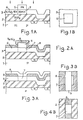
- Zones 6 are obtained where the polycrystalline silicon has a low resistivity of the order of 10 ohms / square and zones 7 located under the resin pins 5 where the polycrystalline silicon has its initial resistivity of the order, for example, of 30 megohms / square.
- the method according to the present invention comprises only two masking steps, namely the step of forming the resin pins 5 illustrated in FIG. 1 A and 1 B, and the step of cutting the bands of tantalum silicide and of polycrystalline silicon illustrated in FIG. 3B and 4B, which makes it possible to obtain resistive elements of minimized dimensions. Furthermore, there is no requirement for rigorous alignment between these two masking steps: as shown in fig. 3B, the existence of a shift between the mask of the pawns and that of the bands has no detrimental influence on the result as long as the transverse dimensions of the pawns have been slightly oversized compared to those of the bands.
- the “lift off” could be carried out of the resin pin 5 and of the tantalum silicide which covers it only after band etching of the tantalum silicide and of the polycrystalline silicon.
Landscapes
- Engineering & Computer Science (AREA)
- Physics & Mathematics (AREA)
- Condensed Matter Physics & Semiconductors (AREA)
- General Physics & Mathematics (AREA)
- Manufacturing & Machinery (AREA)
- Computer Hardware Design (AREA)
- Microelectronics & Electronic Packaging (AREA)
- Power Engineering (AREA)
- Semiconductor Integrated Circuits (AREA)
Applications Claiming Priority (2)
| Application Number | Priority Date | Filing Date | Title |
|---|---|---|---|
| FR8120165 | 1981-10-27 | ||
| FR8120165A FR2515427A1 (fr) | 1981-10-27 | 1981-10-27 | Procede de fabrication de resistances de forte valeur pour circuits integres |
Publications (2)
| Publication Number | Publication Date |
|---|---|
| EP0078190A1 EP0078190A1 (fr) | 1983-05-04 |
| EP0078190B1 true EP0078190B1 (fr) | 1985-07-03 |
Family
ID=9263434
Family Applications (1)
| Application Number | Title | Priority Date | Filing Date |
|---|---|---|---|
| EP82401873A Expired EP0078190B1 (fr) | 1981-10-27 | 1982-10-12 | Procédé de fabrication de résistances de forte valeur pour circuits intégrés |
Country Status (4)
| Country | Link |
|---|---|
| US (1) | US4451328A (show.php) |
| EP (1) | EP0078190B1 (show.php) |
| DE (1) | DE3264575D1 (show.php) |
| FR (1) | FR2515427A1 (show.php) |
Cited By (1)
| Publication number | Priority date | Publication date | Assignee | Title |
|---|---|---|---|---|
| DE3634850A1 (de) * | 1985-10-15 | 1987-04-23 | Mitsubishi Electric Corp | Verfahren zur herstellung einer groesstintegrierten halbleiter-schaltungseinrichtung vom standardscheibentyp |
Families Citing this family (28)
| Publication number | Priority date | Publication date | Assignee | Title |
|---|---|---|---|---|
| US4570328A (en) * | 1983-03-07 | 1986-02-18 | Motorola, Inc. | Method of producing titanium nitride MOS device gate electrode |
| JPS59232456A (ja) * | 1983-06-16 | 1984-12-27 | Hitachi Ltd | 薄膜回路素子 |
| JPS60130844A (ja) * | 1983-12-20 | 1985-07-12 | Toshiba Corp | 半導体装置の製造方法 |
| US4581815A (en) * | 1984-03-01 | 1986-04-15 | Advanced Micro Devices, Inc. | Integrated circuit structure having intermediate metal silicide layer and method of making same |
| US4693925A (en) * | 1984-03-01 | 1987-09-15 | Advanced Micro Devices, Inc. | Integrated circuit structure having intermediate metal silicide layer |
| US4829363A (en) * | 1984-04-13 | 1989-05-09 | Fairchild Camera And Instrument Corp. | Structure for inhibiting dopant out-diffusion |
| US4604789A (en) * | 1985-01-31 | 1986-08-12 | Inmos Corporation | Process for fabricating polysilicon resistor in polycide line |
| DE3683679D1 (de) * | 1985-04-26 | 1992-03-12 | Fujitsu Ltd | Verfahren zur herstellung einer kontaktanordnung fuer eine halbleiteranordnung. |
| US4701241A (en) * | 1986-10-06 | 1987-10-20 | Rca Corporation | Method of making a resistor |
| ATE87766T1 (de) * | 1986-11-18 | 1993-04-15 | Siemens Ag | Integrierte halbleiterschaltung mit als duennschichtstege auf den die aktiven transistorbereiche trennenden feldoxidbereichen angeordneten lastwiderstaende und verfahren zu ihrer herstellung. |
| JPS63136668A (ja) * | 1986-11-28 | 1988-06-08 | Fuji Electric Co Ltd | 半導体装置の製造方法 |
| US4920388A (en) * | 1987-02-17 | 1990-04-24 | Siliconix Incorporated | Power transistor with integrated gate resistor |
| GB8710359D0 (en) * | 1987-05-01 | 1987-06-03 | Inmos Ltd | Semiconductor element |
| JPH01143252A (ja) * | 1987-11-27 | 1989-06-05 | Nec Corp | 半導体装置 |
| US5336911A (en) * | 1988-05-10 | 1994-08-09 | Seiko Epson Corporation | Semiconductor device |
| US4859278A (en) * | 1988-08-11 | 1989-08-22 | Xerox Corporation | Fabrication of high resistive loads utilizing a single level polycide process |
| US5126279A (en) * | 1988-12-19 | 1992-06-30 | Micron Technology, Inc. | Single polysilicon cross-coupled resistor, six-transistor SRAM cell design technique |
| US5017459A (en) * | 1989-04-26 | 1991-05-21 | Eastman Kodak Company | Lift-off process |
| US5135882A (en) * | 1989-07-31 | 1992-08-04 | Micron Technology, Inc. | Technique for forming high-value inter-nodal coupling resistance for rad-hard applications in a double-poly, salicide process using local interconnect |
| US4948747A (en) * | 1989-12-18 | 1990-08-14 | Motorola, Inc. | Method of making an integrated circuit resistor |
| US5068201A (en) * | 1990-05-31 | 1991-11-26 | Sgs-Thomson Microelectronics, Inc. | Method for forming a high valued resistive load element and low resistance interconnect for integrated circuits |
| USD332204S (en) | 1991-01-31 | 1993-01-05 | The Decor Corporation Pty. Ltd. | Combined container lid and convertible grid |
| JPH088225B2 (ja) * | 1991-12-17 | 1996-01-29 | インターナショナル・ビジネス・マシーンズ・コーポレイション | 改良された半導体用局部的相互接続 |
| US6143613A (en) * | 1997-06-30 | 2000-11-07 | Vlsi Technology, Inc. | Selective exclusion of silicide formation to make polysilicon resistors |
| US6023086A (en) * | 1997-09-02 | 2000-02-08 | Motorola, Inc. | Semiconductor transistor with stabilizing gate electrode |
| US6187617B1 (en) | 1999-07-29 | 2001-02-13 | International Business Machines Corporation | Semiconductor structure having heterogeneous silicide regions and method for forming same |
| US20050130383A1 (en) * | 2003-12-10 | 2005-06-16 | International Business Machines Corporation | Silicide resistor in beol layer of semiconductor device and method |
| US7393701B2 (en) * | 2006-12-05 | 2008-07-01 | International Business Machines Corporation | Method of adjusting buried resistor resistance |
Family Cites Families (8)
| Publication number | Priority date | Publication date | Assignee | Title |
|---|---|---|---|---|
| GB1501114A (en) * | 1974-04-25 | 1978-02-15 | Rca Corp | Method of making a semiconductor device |
| US4214917A (en) * | 1978-02-10 | 1980-07-29 | Emm Semi | Process of forming a semiconductor memory cell with continuous polysilicon run circuit elements |
| US4297721A (en) * | 1978-11-03 | 1981-10-27 | Mostek Corporation | Extremely low current load device for integrated circuit |
| US4332839A (en) * | 1978-12-29 | 1982-06-01 | Bell Telephone Laboratories, Incorporated | Method for making integrated semiconductor circuit structure with formation of Ti or Ta silicide |
| US4267558A (en) * | 1979-01-05 | 1981-05-12 | Texas Instruments Incorporated | Electrically erasable memory with self-limiting erase |
| JPS5599722A (en) * | 1979-01-26 | 1980-07-30 | Hitachi Ltd | Preparation of semiconductor device |
| US4291328A (en) * | 1979-06-15 | 1981-09-22 | Texas Instruments Incorporated | Interlevel insulator for integrated circuit with implanted resistor element in second-level polycrystalline silicon |
| US4362597A (en) * | 1981-01-19 | 1982-12-07 | Bell Telephone Laboratories, Incorporated | Method of fabricating high-conductivity silicide-on-polysilicon structures for MOS devices |
-
1981
- 1981-10-27 FR FR8120165A patent/FR2515427A1/fr active Granted
-
1982
- 1982-09-27 US US06/423,722 patent/US4451328A/en not_active Expired - Lifetime
- 1982-10-12 DE DE8282401873T patent/DE3264575D1/de not_active Expired
- 1982-10-12 EP EP82401873A patent/EP0078190B1/fr not_active Expired
Cited By (1)
| Publication number | Priority date | Publication date | Assignee | Title |
|---|---|---|---|---|
| DE3634850A1 (de) * | 1985-10-15 | 1987-04-23 | Mitsubishi Electric Corp | Verfahren zur herstellung einer groesstintegrierten halbleiter-schaltungseinrichtung vom standardscheibentyp |
Also Published As
| Publication number | Publication date |
|---|---|
| DE3264575D1 (en) | 1985-08-08 |
| FR2515427A1 (fr) | 1983-04-29 |
| EP0078190A1 (fr) | 1983-05-04 |
| US4451328A (en) | 1984-05-29 |
| FR2515427B1 (show.php) | 1983-12-02 |
Similar Documents
| Publication | Publication Date | Title |
|---|---|---|
| EP0078190B1 (fr) | Procédé de fabrication de résistances de forte valeur pour circuits intégrés | |
| EP0203836B1 (fr) | Procédé de fabrication de transistors à effet de champ, et transistors bipolaires latéraux sur un même substrat | |
| US4446613A (en) | Integrated circuit resistor and method of fabrication | |
| FR2822293A1 (fr) | Transistor a effet de champ et double grille, circuit integre comportant ce transistor, et procede de fabrication de ce dernier | |
| KR20020078677A (ko) | 선택적 결정 성장을 이용한 반도체 장치 제조 방법 | |
| US7709336B2 (en) | Metal hard mask method and structure for strained silicon MOS transistors | |
| FR2583920A1 (fr) | Procede de fabrication d'un circuit integre et notamment d'une memoire eprom comportant deux composants distincts isoles electriquement | |
| CN1266747C (zh) | 有助于残留物去除的各向同性电阻器保护蚀刻 | |
| EP0522938B1 (fr) | Procédé de fabrication d'un transistor à effet de champ vertical, et transistor obtenu par ce procédé | |
| KR100207548B1 (ko) | 반도체장치의 제조공정에서 게이트 전극 형성방법 | |
| CN1832140B (zh) | 用于图像传感器的自对准金属硅化物处理方法 | |
| KR20050029881A (ko) | 반도체 소자의 실리사이드 형성방법 | |
| KR100559572B1 (ko) | 살리사이드를 갖는 반도체 소자 제조 방법 | |
| KR20030079806A (ko) | 적층형 게이트 전극을 갖는 반도체 장치의 제조 방법 | |
| FR2871294A1 (fr) | Procede de realisation d'un transistor dmos de taille reduite, et transistor dmos en resultant | |
| EP0065464B1 (fr) | Procédé de fabrication de circuits intégrés de type MOS | |
| FR2842944A1 (fr) | Procede de formation d'ouvertures de contact sur un circuit integre mos | |
| KR100552859B1 (ko) | 반도체 소자의 제조 방법 | |
| FR2578097A1 (fr) | Procede de fabrication de circuits integres en technologie mos et cmos et structure cmos correspondante | |
| KR100927787B1 (ko) | 반도체 소자 제조 방법 | |
| EP0024222B1 (fr) | Procédé de fabrication d'un transistor à effet de champ à grille SCHOTTKY autoalignée | |
| KR20060031953A (ko) | 반도체 소자의 제조 방법 | |
| EP0194193A1 (fr) | Procédé de fabrication d'un circuit intégré à transistors MOS à électrodes en siliciure métallique | |
| FR2621738A1 (fr) | Structure de transistor a effet de champ a grille metallique isolee et procede de fabrication | |
| JPH04245643A (ja) | 半導体装置の製造方法 |
Legal Events
| Date | Code | Title | Description |
|---|---|---|---|
| PUAI | Public reference made under article 153(3) epc to a published international application that has entered the european phase |
Free format text: ORIGINAL CODE: 0009012 |
|
| AK | Designated contracting states |
Designated state(s): CH DE FR GB IT LI NL |
|
| 17P | Request for examination filed |
Effective date: 19830511 |
|
| ITF | It: translation for a ep patent filed | ||
| GRAA | (expected) grant |
Free format text: ORIGINAL CODE: 0009210 |
|
| AK | Designated contracting states |
Designated state(s): CH DE FR GB IT LI NL |
|
| REF | Corresponds to: |
Ref document number: 3264575 Country of ref document: DE Date of ref document: 19850808 |
|
| PLBE | No opposition filed within time limit |
Free format text: ORIGINAL CODE: 0009261 |
|
| STAA | Information on the status of an ep patent application or granted ep patent |
Free format text: STATUS: NO OPPOSITION FILED WITHIN TIME LIMIT |
|
| 26N | No opposition filed | ||
| PGFP | Annual fee paid to national office [announced via postgrant information from national office to epo] |
Ref country code: NL Payment date: 19901031 Year of fee payment: 9 |
|
| PGFP | Annual fee paid to national office [announced via postgrant information from national office to epo] |
Ref country code: CH Payment date: 19911025 Year of fee payment: 10 |
|
| ITTA | It: last paid annual fee | ||
| PG25 | Lapsed in a contracting state [announced via postgrant information from national office to epo] |
Ref country code: NL Effective date: 19920501 |
|
| NLV4 | Nl: lapsed or anulled due to non-payment of the annual fee | ||
| PG25 | Lapsed in a contracting state [announced via postgrant information from national office to epo] |
Ref country code: LI Effective date: 19921031 Ref country code: CH Effective date: 19921031 |
|
| REG | Reference to a national code |
Ref country code: CH Ref legal event code: PL |
|
| REG | Reference to a national code |
Ref country code: FR Ref legal event code: D6 |
|
| PGFP | Annual fee paid to national office [announced via postgrant information from national office to epo] |
Ref country code: GB Payment date: 20011024 Year of fee payment: 20 |
|
| PGFP | Annual fee paid to national office [announced via postgrant information from national office to epo] |
Ref country code: FR Payment date: 20011025 Year of fee payment: 20 |
|
| PGFP | Annual fee paid to national office [announced via postgrant information from national office to epo] |
Ref country code: DE Payment date: 20011029 Year of fee payment: 20 |
|
| REG | Reference to a national code |
Ref country code: GB Ref legal event code: IF02 |
|
| PG25 | Lapsed in a contracting state [announced via postgrant information from national office to epo] |
Ref country code: GB Free format text: LAPSE BECAUSE OF EXPIRATION OF PROTECTION Effective date: 20021011 |
|
| REG | Reference to a national code |
Ref country code: GB Ref legal event code: PE20 Effective date: 20021011 |