EP0078087A2 - Decodierung von binär-codierten Bildfarbsignalen - Google Patents
Decodierung von binär-codierten Bildfarbsignalen Download PDFInfo
- Publication number
- EP0078087A2 EP0078087A2 EP82201336A EP82201336A EP0078087A2 EP 0078087 A2 EP0078087 A2 EP 0078087A2 EP 82201336 A EP82201336 A EP 82201336A EP 82201336 A EP82201336 A EP 82201336A EP 0078087 A2 EP0078087 A2 EP 0078087A2
- Authority
- EP
- European Patent Office
- Prior art keywords
- analogue
- inputs
- arrangement
- switches
- colour video
- Prior art date
- Legal status (The legal status is an assumption and is not a legal conclusion. Google has not performed a legal analysis and makes no representation as to the accuracy of the status listed.)
- Withdrawn
Links
Images
Classifications
-
- G—PHYSICS
- G09—EDUCATION; CRYPTOGRAPHY; DISPLAY; ADVERTISING; SEALS
- G09G—ARRANGEMENTS OR CIRCUITS FOR CONTROL OF INDICATING DEVICES USING STATIC MEANS TO PRESENT VARIABLE INFORMATION
- G09G1/00—Control arrangements or circuits, of interest only in connection with cathode-ray tube indicators; General aspects or details, e.g. selection emphasis on particular characters, dashed line or dotted line generation; Preprocessing of data
- G09G1/28—Control arrangements or circuits, of interest only in connection with cathode-ray tube indicators; General aspects or details, e.g. selection emphasis on particular characters, dashed line or dotted line generation; Preprocessing of data using colour tubes
- G09G1/285—Interfacing with colour displays, e.g. TV receiver
-
- G—PHYSICS
- G09—EDUCATION; CRYPTOGRAPHY; DISPLAY; ADVERTISING; SEALS
- G09G—ARRANGEMENTS OR CIRCUITS FOR CONTROL OF INDICATING DEVICES USING STATIC MEANS TO PRESENT VARIABLE INFORMATION
- G09G1/00—Control arrangements or circuits, of interest only in connection with cathode-ray tube indicators; General aspects or details, e.g. selection emphasis on particular characters, dashed line or dotted line generation; Preprocessing of data
- G09G1/28—Control arrangements or circuits, of interest only in connection with cathode-ray tube indicators; General aspects or details, e.g. selection emphasis on particular characters, dashed line or dotted line generation; Preprocessing of data using colour tubes
Definitions
- the invention relates to a colour video signal decoder circuit arrangement for decoding a binary coded colour video signal and producing an analogue colour video signal therefrom, said arrangement comprising a plurality of input ports equal in number to the number of components forming the binary coded colour video signal, with each port having a number (n) of input terminals for receiving one of the components of the colour video signal as a multi-bit binary code in parallel each combination of the parallel binary code representing a respective amplitude of said component, each port being connected to an associated selector circuit for selecting a particular one of m outputs (where ni ⁇ 2n) which can be uniquely identified by respective combinations of the parallel binary inputs at the associated port, characterised in that such an arrangement is disclosed in United Kingdom Patent Application 2 005 500A which relates to a video signal synthesiser for a digital video display system.
- Figure 8 of that application discloses a digital- to-analogue converter for producing an analogue monochrome video signal from a binary coded monochrome signal where the binary code combinations are used to control which of a number of resistors are connected in parallel, the paralleled resistors forming the upper component of a voltage divider the lower component of which is formed by a load resistance across which the analogue output is formed.
- the specification states that its features can be employed with a colour system. However, if the converter of the Figure 8 were to be used with a colour video signal there would in fact need to be three such converters for the red, green and blue colour components respectively which besides leading to the considerable number of resistors required would not provide accurate tracing between the three converters.
- the invention provides a decoder circuit arrangement for decoding binary coded colour video signals and producing analogue colour video signals therefrom, said arrangement comprising a plurality of input ports equal in number to the number of components forming the binary coded colour video signal with each port having a number (n) of input terminals for receiving one of the components of the colour video signal as a multi-bit binary code in parallel each combination of the parallel binary code representing a respective amplitude of said component, each port being connected to an associated selector circuit for selecting a particular one of m outputs (where m.. ⁇ 2 n) which can be uniquely identified by respective combinations of the parallel binary inputs at the associated port, characterised in that the outputs of the selector circuit are individually connected to respective control inputs of m analogue switches in a group such that a different one only of said switches in a group is rendered conductive for each code combination, a common reference supply arrangement having a chain of m points each providing a different reference level which reference levels have a given relationship, each reference level point being connected to the
- the relationship between the reference levels may be such that an equal increment is present between adjacent reference level points.
- the relationship between the reference levels may be such that the increments between adjacent reference level points are not equal, each commoned output producing a component which is gamma corrected.
- the output may however follow some other desired law.
- the reference supply arrangement may be a voltage supply arrangement and may comprise a potential divider connected between first and second terminals for receiving a stablised voltage supply, which first and second terminals also form two of the reference voltage level points.
- a reference voltage supply arrangement may comprise a potential divider connected between first and second terminals which terminals also form two of the reference voltage level points, said terminals being connected to a voltage supply whose voltage is adapted to be changed to produce a consequent change in the intensity of the hue resulting from the components at the commoned outputs. If resistors were to be used in the potential divider then less than one third of those required with the prior art arrangement would be needed.
- the reference supply arrangement may be a current supply arrangement for providing reference currents of different levels.
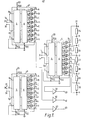
- the references 1,2 and 3 indicate three inputs which together form a port for receiving a parallel binary signal coded by the red component of a colour video signal. These inputs are respectively connected to the input terminals A O' A and A 2 of an 8-channel analogue multiplexer/demultiplexer 4 which may be of the Philips Type HEF 4051B as described in the Philips Data Handbook, Integrated circuits, Part 4, October 1980 "Digital integated circuit - LOCMOS HE 4000B family" pages 311 to 318 which are incorporated herein by way of reference.
- the three input terminals are connected to an analogue level conversion circuit 5 which produces a suitable shift in the level of the binary input signals to provide the necessary drive for a selector circuit 6.
- the selector circuit 6 is a I-out-of-8 decoder which selects a particular one out of the eight outputs which can be uniquely identified by the respective combinations of the parallel binary coded inputs at the inputs 1, 2 and 3. These outputs individually appear one at a time, on output lines 7-14 inclusive and which are connected to the control input of individual analogue switches 15-22 respectively, a respective output from a selector circuit thus causing the respective analogue switch to become conducting with the remaining switches then being non-conducting.
- a terminal 23 connected to the multiplexer's V DD terminal and hence to the conversion circuit 5 and selector circuit 6 is connected to a positive d.c.
- the analogue switches 15-22 are respectively connected to switch input terminals Y -Y , of the multiplexer, these input terminals being respectively connected to points A-H on a voltage divider formed by resistors 24-30, the lower end of resistor 30 and point H being connected to earth, whilst the upper end of resistor 24 and point A are connected to a d.c. voltage reference source of 2 volts by means of a terminal 31.
- the outputs of the analogue switches 15-22 are commoned and taken to a multiplexer output terminal Z which is connected through a buffer amplifier 32 having a high input impedance to an output 33.
- the various code combinations of the binary coded signal applied to the inputs 1, 2 and 3 represent eight different amplitude levels for the red colour component. If the resistors 24-30 each have the same value then the voltage present at the various points from H to A on the voltage divider will increase by equal amounts.
- the various combinations of the binary coded signal will cause the individual switches to be closed as required to cause the voltages at the points on the voltage divider connected to the closed switches to be successively present at terminal Z.
- each analogue switch 15-22 effectively includes a series resistance of some 50 to 100 ohms in its conductive path and the inclusion of the buffer amplifier 32 of high input impedance between the terminal Z and the output 33 substantially reduces the voltage drop across that series resistance and the current drain from the potential divider.
- the buffer amplifier 32 may be dispensed with.
- these resistors may be given different values in which case the voltage levels on the points A-H and hence that at the output 43 would follow a given law, such as one required for gamma correction.
- the arrangement of Figure 1 is further provided with second and third 8-channel analogue multiplexers 4' and 4" which are of the same construction and type as that of multiplexer 4.
- the corresponding parts of the multiplexer 4' and 4" bear the same reference numbers as the multiplexer 4 and function in exactly the same manner.
- the multiplexer 4' has its three input terminals A 0 , A. and A 2 respectively connected to inputs 34, 35 and 36, these inputs receiving a parallel binary signal coded by the blue component of the colour video signal.
- the multiplexer 4" has its three input terminals A 0 , A 1 and A 2 respectively connected to inputs 37, 38 and 39 which inputs receive a parallel binary signal coded by the green component of the colour video signal.
- the input terminals Y O -Y 7 of the analogue switches 15-22 of the multiplexers 4' and 4" are connected to the same points A-H on the voltage divider 24-30 as are the corresponding input terminals for the multiplexer 4.
- the output terminal Z of the multiplexer 4' is connected through a buffer amplifier 40 to an output 41 at which will be found an analogue blue component whilst the output terminal Z of the multiplexer 4" is connected through a buffer amplifier 42 to an output 43 at which an analogue green component is produced.
- the red, blue and green components at the respective outputs 33, 41 and 43 may be further processed e.g. by respective video amplifier stages, before the colour signal is displayed.
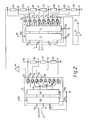
- Figure 2 shows a modification of part of Figure 1 and like references between the two figures indicate like components.
- the multiplexers 4' and 4", their inputs and other connections, and their associated buffer amplifiers and outputs have been omitted.
- the point A and upper terminal of resistor 24 are not connected to a constant d.c. voltage reference source as is the case for Figure 1 but instead are connected to the output of a buffer amplifier 44, whose high impedance input is connected to the output terminal Z A of dual 4-channel analogue multiplexer/demultiplexer 45 which may be of the Philips HEF 4052B details of which can be found between pages 319 to 326 of the above mentioned Philips Data Handbook which are incorporated herein by way of reference.
- the multiplexer 45 has two input terminals A 0 , A connected to inputs 46 and 47 which convey a parallel two bit binary code whose different binary word combinations denote different reference voltages which may be applied to the voltage divider 24-30.
- the input terminals AO and A 1 of the multiplexer 45 are applied to a logic level conversion circuit 48 which in turn is connected to a selector circuit 49 for similarly producing an individual control signal for one of four switches 50-53.
- these control signals are also individually connected to four further analogue switches 54-57 which are not employed in the arrangement of Figure 2.
- the multiplexer's terminals Y 0A - Y 3A for the inputs of the switches 50-53 are connected to points U, V, W, and X of a second voltage divider formed by resistors 58, 59 and 60 which are connected between a terminal 61 for a source of d.c. constant reference voltage of 2 volts, and earth.
- the voltage from the voltage divider 58-60 appearing at the common output terminal Z A of switches 50-53 is dependent on the binary code combinations applied to inputs 46 and 47 and this in turn determines the voltage applied to the voltage divider 24-30 for the multiplexers 4, 4' and 4".
- the voltage applied to the voltage divider 24-30 will cause a step-wise change in intensity of the hue of the final colour combination.
- Figure 2 only two inputs are shown for the multiplexer 45 to produce four different levels for the voltage from buffer amplifier 44.
- the number of inputs may be increased to increase the number of levels produced at the output so that a more gradual change in level can be obtained to produce any desired change of the resulting output voltage.
- variable voltage supply for the voltage divider 24-30 is derived from an analogue multiplexer/demultiplexer, it may be obtained in other ways which provide decoding of a digital signal to produce its analogue counterpart.
- the binary inputs for such a decoding arrangement may be derived from a microprocessor or other form of digital control circuitry.
- the inputs for the multiplexers 4, 4' and 4" relate to the red, blue and green components of a colour video signal. There is no reason why these inputs should not relate to some other combination to produce the required hues and their intensities.
- the three inputs might then be two colour different signals (R-Y) and (B-Y) and a luminance signal Y.
Landscapes
- Engineering & Computer Science (AREA)
- Radar, Positioning & Navigation (AREA)
- Remote Sensing (AREA)
- Physics & Mathematics (AREA)
- Computer Hardware Design (AREA)
- General Physics & Mathematics (AREA)
- Theoretical Computer Science (AREA)
- Processing Of Color Television Signals (AREA)
- Color Television Systems (AREA)
Applications Claiming Priority (2)
| Application Number | Priority Date | Filing Date | Title |
|---|---|---|---|
| GB8132450 | 1981-10-28 | ||
| GB08132450A GB2108341B (en) | 1981-10-28 | 1981-10-28 | Decoding binary coded colour video signals |
Publications (2)
| Publication Number | Publication Date |
|---|---|
| EP0078087A2 true EP0078087A2 (de) | 1983-05-04 |
| EP0078087A3 EP0078087A3 (de) | 1983-11-30 |
Family
ID=10525448
Family Applications (1)
| Application Number | Title | Priority Date | Filing Date |
|---|---|---|---|
| EP82201336A Withdrawn EP0078087A3 (de) | 1981-10-28 | 1982-10-26 | Decodierung von binär-codierten Bildfarbsignalen |
Country Status (4)
| Country | Link |
|---|---|
| EP (1) | EP0078087A3 (de) |
| JP (1) | JPS58100588A (de) |
| GB (1) | GB2108341B (de) |
| HK (1) | HK19186A (de) |
Family Cites Families (3)
| Publication number | Priority date | Publication date | Assignee | Title |
|---|---|---|---|---|
| JPS5228851A (en) * | 1975-08-29 | 1977-03-04 | Nat Semiconductor Corp | Converter circuit |
| GB2005500B (en) * | 1977-09-26 | 1982-07-14 | Burroughs Corp | Video synthesizer for digital video display system employiing a plurality of gray-scale levels |
| US4183046A (en) * | 1978-08-17 | 1980-01-08 | Interpretation Systems Incorporated | Electronic apparatus for converting digital image or graphics data to color video display formats and method therefor |
-
1981
- 1981-10-28 GB GB08132450A patent/GB2108341B/en not_active Expired
-
1982
- 1982-10-25 JP JP57186219A patent/JPS58100588A/ja active Pending
- 1982-10-26 EP EP82201336A patent/EP0078087A3/de not_active Withdrawn
-
1986
- 1986-03-20 HK HK19186A patent/HK19186A/xx unknown
Also Published As
| Publication number | Publication date |
|---|---|
| JPS58100588A (ja) | 1983-06-15 |
| EP0078087A3 (de) | 1983-11-30 |
| GB2108341A (en) | 1983-05-11 |
| GB2108341B (en) | 1984-12-12 |
| HK19186A (en) | 1986-03-27 |
Similar Documents
| Publication | Publication Date | Title |
|---|---|---|
| KR100304955B1 (ko) | 디지털/아날로그변환기 | |
| KR100186679B1 (ko) | 디지탈-아날로그 변환회로 | |
| US4636772A (en) | Multiple function type D/A converter | |
| EP0322965B1 (de) | Digital/Analog-Wandler | |
| CA1259705A (en) | Digital-to-analog converter | |
| US6674413B2 (en) | Display control apparatus | |
| US4396907A (en) | Digital to analog converter which uses main and auxiliary resistor networks | |
| JP3037766B2 (ja) | ディジタル−アナログ変換器 | |
| US4896157A (en) | Digital to analog converter having single resistive string with shiftable voltage thereacross | |
| EP0331172A2 (de) | Bezugsgenerator | |
| US5633637A (en) | Digital-to-analog converter circuit | |
| US5894281A (en) | Digital-to-analog converter utilizing MOS transistor switching circuit with accompanying dummy gates to set same effective gate capacitance | |
| US3582941A (en) | Nonlinear decoder | |
| GB2102644A (en) | Circuit arrangement for producing analogue television signals with amplitude adjustment | |
| US6344815B2 (en) | Digital-to-analog converter | |
| EP0078087A2 (de) | Decodierung von binär-codierten Bildfarbsignalen | |
| KR20090031184A (ko) | 디지털 투 아날로그 컨버터 | |
| US4346399A (en) | Color temperature control circuit | |
| US4511881A (en) | Integrated voltage divider with selection circuit | |
| KR100454860B1 (ko) | 디지털 아날로그 변환기 | |
| US4641131A (en) | Circuit arrangement for converting a digital input signal into an analog output signal | |
| KR19980065270A (ko) | 저항열을 이용한 디지탈-아날로그 변환기 | |
| CA1244137A (en) | Input ranging divider and method for an analog to digital converter | |
| JPS60216630A (ja) | ステツプ発生器 | |
| JP2628083B2 (ja) | ディジタルアナログ変換器 |
Legal Events
| Date | Code | Title | Description |
|---|---|---|---|
| PUAI | Public reference made under article 153(3) epc to a published international application that has entered the european phase |
Free format text: ORIGINAL CODE: 0009012 |
|
| 17P | Request for examination filed |
Effective date: 19821026 |
|
| AK | Designated contracting states |
Designated state(s): DE FR GB |
|
| PUAL | Search report despatched |
Free format text: ORIGINAL CODE: 0009013 |
|
| AK | Designated contracting states |
Designated state(s): DE FR GB |
|
| STAA | Information on the status of an ep patent application or granted ep patent |
Free format text: STATUS: THE APPLICATION HAS BEEN WITHDRAWN |
|
| 18W | Application withdrawn |
Withdrawal date: 19850510 |
|
| RIN1 | Information on inventor provided before grant (corrected) |
Inventor name: WONG, KWOK KEUNG |