EP0078037B1 - Lampe mit lichtemittierenden Dioden und Verfahren zum Herstellen - Google Patents
Lampe mit lichtemittierenden Dioden und Verfahren zum Herstellen Download PDFInfo
- Publication number
- EP0078037B1 EP0078037B1 EP82109788A EP82109788A EP0078037B1 EP 0078037 B1 EP0078037 B1 EP 0078037B1 EP 82109788 A EP82109788 A EP 82109788A EP 82109788 A EP82109788 A EP 82109788A EP 0078037 B1 EP0078037 B1 EP 0078037B1
- Authority
- EP
- European Patent Office
- Prior art keywords
- conductive means
- cap
- light emission
- emission diode
- base member
- Prior art date
- Legal status (The legal status is an assumption and is not a legal conclusion. Google has not performed a legal analysis and makes no representation as to the accuracy of the status listed.)
- Expired
Links
Images

Classifications
-
- H—ELECTRICITY
- H01—ELECTRIC ELEMENTS
- H01L—SEMICONDUCTOR DEVICES NOT COVERED BY CLASS H10
- H01L33/00—Semiconductor devices with at least one potential-jump barrier or surface barrier specially adapted for light emission; Processes or apparatus specially adapted for the manufacture or treatment thereof or of parts thereof; Details thereof
- H01L33/48—Semiconductor devices with at least one potential-jump barrier or surface barrier specially adapted for light emission; Processes or apparatus specially adapted for the manufacture or treatment thereof or of parts thereof; Details thereof characterised by the semiconductor body packages
- H01L33/483—Containers
-
- F—MECHANICAL ENGINEERING; LIGHTING; HEATING; WEAPONS; BLASTING
- F21—LIGHTING
- F21K—NON-ELECTRIC LIGHT SOURCES USING LUMINESCENCE; LIGHT SOURCES USING ELECTROCHEMILUMINESCENCE; LIGHT SOURCES USING CHARGES OF COMBUSTIBLE MATERIAL; LIGHT SOURCES USING SEMICONDUCTOR DEVICES AS LIGHT-GENERATING ELEMENTS; LIGHT SOURCES NOT OTHERWISE PROVIDED FOR
- F21K9/00—Light sources using semiconductor devices as light-generating elements, e.g. using light-emitting diodes [LED] or lasers
- F21K9/20—Light sources comprising attachment means
- F21K9/23—Retrofit light sources for lighting devices with a single fitting for each light source, e.g. for substitution of incandescent lamps with bayonet or threaded fittings
-
- H—ELECTRICITY
- H01—ELECTRIC ELEMENTS
- H01L—SEMICONDUCTOR DEVICES NOT COVERED BY CLASS H10
- H01L24/00—Arrangements for connecting or disconnecting semiconductor or solid-state bodies; Methods or apparatus related thereto
- H01L24/93—Batch processes
- H01L24/95—Batch processes at chip-level, i.e. with connecting carried out on a plurality of singulated devices, i.e. on diced chips
- H01L24/97—Batch processes at chip-level, i.e. with connecting carried out on a plurality of singulated devices, i.e. on diced chips the devices being connected to a common substrate, e.g. interposer, said common substrate being separable into individual assemblies after connecting
-
- H—ELECTRICITY
- H01—ELECTRIC ELEMENTS
- H01L—SEMICONDUCTOR DEVICES NOT COVERED BY CLASS H10
- H01L25/00—Assemblies consisting of a plurality of individual semiconductor or other solid state devices ; Multistep manufacturing processes thereof
- H01L25/03—Assemblies consisting of a plurality of individual semiconductor or other solid state devices ; Multistep manufacturing processes thereof all the devices being of a type provided for in the same subgroup of groups H01L27/00 - H01L33/00, or in a single subclass of H10K, H10N, e.g. assemblies of rectifier diodes
- H01L25/04—Assemblies consisting of a plurality of individual semiconductor or other solid state devices ; Multistep manufacturing processes thereof all the devices being of a type provided for in the same subgroup of groups H01L27/00 - H01L33/00, or in a single subclass of H10K, H10N, e.g. assemblies of rectifier diodes the devices not having separate containers
- H01L25/075—Assemblies consisting of a plurality of individual semiconductor or other solid state devices ; Multistep manufacturing processes thereof all the devices being of a type provided for in the same subgroup of groups H01L27/00 - H01L33/00, or in a single subclass of H10K, H10N, e.g. assemblies of rectifier diodes the devices not having separate containers the devices being of a type provided for in group H01L33/00
- H01L25/0753—Assemblies consisting of a plurality of individual semiconductor or other solid state devices ; Multistep manufacturing processes thereof all the devices being of a type provided for in the same subgroup of groups H01L27/00 - H01L33/00, or in a single subclass of H10K, H10N, e.g. assemblies of rectifier diodes the devices not having separate containers the devices being of a type provided for in group H01L33/00 the devices being arranged next to each other
-
- F—MECHANICAL ENGINEERING; LIGHTING; HEATING; WEAPONS; BLASTING
- F21—LIGHTING
- F21Y—INDEXING SCHEME ASSOCIATED WITH SUBCLASSES F21K, F21L, F21S and F21V, RELATING TO THE FORM OR THE KIND OF THE LIGHT SOURCES OR OF THE COLOUR OF THE LIGHT EMITTED
- F21Y2115/00—Light-generating elements of semiconductor light sources
- F21Y2115/10—Light-emitting diodes [LED]
-
- H—ELECTRICITY
- H01—ELECTRIC ELEMENTS
- H01L—SEMICONDUCTOR DEVICES NOT COVERED BY CLASS H10
- H01L2224/00—Indexing scheme for arrangements for connecting or disconnecting semiconductor or solid-state bodies and methods related thereto as covered by H01L24/00
- H01L2224/01—Means for bonding being attached to, or being formed on, the surface to be connected, e.g. chip-to-package, die-attach, "first-level" interconnects; Manufacturing methods related thereto
- H01L2224/42—Wire connectors; Manufacturing methods related thereto
- H01L2224/47—Structure, shape, material or disposition of the wire connectors after the connecting process
- H01L2224/48—Structure, shape, material or disposition of the wire connectors after the connecting process of an individual wire connector
- H01L2224/481—Disposition
- H01L2224/48151—Connecting between a semiconductor or solid-state body and an item not being a semiconductor or solid-state body, e.g. chip-to-substrate, chip-to-passive
- H01L2224/48221—Connecting between a semiconductor or solid-state body and an item not being a semiconductor or solid-state body, e.g. chip-to-substrate, chip-to-passive the body and the item being stacked
- H01L2224/48245—Connecting between a semiconductor or solid-state body and an item not being a semiconductor or solid-state body, e.g. chip-to-substrate, chip-to-passive the body and the item being stacked the item being metallic
- H01L2224/48247—Connecting between a semiconductor or solid-state body and an item not being a semiconductor or solid-state body, e.g. chip-to-substrate, chip-to-passive the body and the item being stacked the item being metallic connecting the wire to a bond pad of the item
-
- H—ELECTRICITY
- H01—ELECTRIC ELEMENTS
- H01L—SEMICONDUCTOR DEVICES NOT COVERED BY CLASS H10
- H01L2224/00—Indexing scheme for arrangements for connecting or disconnecting semiconductor or solid-state bodies and methods related thereto as covered by H01L24/00
- H01L2224/01—Means for bonding being attached to, or being formed on, the surface to be connected, e.g. chip-to-package, die-attach, "first-level" interconnects; Manufacturing methods related thereto
- H01L2224/42—Wire connectors; Manufacturing methods related thereto
- H01L2224/47—Structure, shape, material or disposition of the wire connectors after the connecting process
- H01L2224/49—Structure, shape, material or disposition of the wire connectors after the connecting process of a plurality of wire connectors
- H01L2224/491—Disposition
- H01L2224/4911—Disposition the connectors being bonded to at least one common bonding area, e.g. daisy chain
- H01L2224/49113—Disposition the connectors being bonded to at least one common bonding area, e.g. daisy chain the connectors connecting different bonding areas on the semiconductor or solid-state body to a common bonding area outside the body, e.g. converging wires
-
- H—ELECTRICITY
- H01—ELECTRIC ELEMENTS
- H01L—SEMICONDUCTOR DEVICES NOT COVERED BY CLASS H10
- H01L2924/00—Indexing scheme for arrangements or methods for connecting or disconnecting semiconductor or solid-state bodies as covered by H01L24/00
- H01L2924/10—Details of semiconductor or other solid state devices to be connected
- H01L2924/11—Device type
- H01L2924/12—Passive devices, e.g. 2 terminal devices
- H01L2924/1204—Optical Diode
- H01L2924/12041—LED
-
- Y—GENERAL TAGGING OF NEW TECHNOLOGICAL DEVELOPMENTS; GENERAL TAGGING OF CROSS-SECTIONAL TECHNOLOGIES SPANNING OVER SEVERAL SECTIONS OF THE IPC; TECHNICAL SUBJECTS COVERED BY FORMER USPC CROSS-REFERENCE ART COLLECTIONS [XRACs] AND DIGESTS
- Y10—TECHNICAL SUBJECTS COVERED BY FORMER USPC
- Y10S—TECHNICAL SUBJECTS COVERED BY FORMER USPC CROSS-REFERENCE ART COLLECTIONS [XRACs] AND DIGESTS
- Y10S362/00—Illumination
- Y10S362/80—Light emitting diode
Definitions
- the present invention relates to an illumination light source device using a light emission diode (LED) (hereinafter referred to as LED-lamp) and a method for producing thereof.
- LED light emission diode
- a conventional small-sized incandescent lamp has a lamp cap or base with thread (Edision type) or with protrusions (swan type) which may be received in a socket of the Edison type or the swan type respectively.
- An LED is not provided with such a base or cap and therefore it is very troublesome to mount in an apparatus as an LED-lamp or substitute for a conventional small-sized incandescent lamp.
- a light emitting diode includes two conductive means, one conductive means being connected through a resistor to a contact member provided from the outer surface of a casing and the other conductive means being connected with the casing.
- prior art document Research Disclosure, No. 191, March 1980, Abstract 19107 describes a light source which is similar to that of prior art document DE-A-2,818,973.
- this light source one terminal of a light emitting diode is connected to a conduct point through a resistor, wherein an insulator is provided between this terminal and a casing.
- the other terminal of the light emitting diode is connected with the casing.
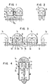
- Figs. 1 and 2 show an example of conventional LED.
- the LED are produced in such a manner that a plurality of sets of conductors connected in the form of train is punched out successively from an electrically conductive sheet by using a drill-press, each set including a pair of T-shaped conductors A, A each having a lead strip portion A 2 and a substrate portion A 1 (hereinafter each conductor being referred to as a lead-substrate).
- an LED element B is electrically attached onto the substrate portion A 1 of one of the pair of lead-substrate A, A successively in each of the series connected conductor sets and electrically connected to the other substrate portion A 1 by a lead wire C. Then, the LED element B is embedded in a molding of a light-transmissible resin material D together with the substrate portions A 2 , A 2 , the lead wire C and parts of the lead strip portions A 2 , A 2 in every set successively. Finally, connection portions A3 connecting adjacent ones of lead strip portions A 2 , A 2 are cut off to obtain an individual LED as shown in Fig. 2.
- Such a conventional LED-lamp as shown in Fig. 2 has no lamp cap or base and therefore it can not be received by a socket which has been already mounted on an apparatus. Thus, it is very troublesome to attach or mount such an LED-lamp onto an apparatus. Further, since the operating voltage of an LED is low when it is separately used, it may be necessary to connect a resistor in series with the LED-lamp, resulting in much trouble in wiring working.
- FIGs. 3 to 5 illustrate a first embodiment of the present invention.
- An LED-lamp unit L comprises three aligned and parallely extending lead-substrates, central one of which is represented by numeral 2 and each of outer two of which by numeral 1.
- the LED lamps unit L of this embodiment of the present invention is produced in such a manner that a plurality sets of lead-substrates connected through connection portions 3 in the form of train is first puched out successively from a conductive sheet by using a drill-press, each set including the above-mentioned three lead-substrates 1, 2, 1, as shown in Fig. 3.
- the lead-substrates 1, 2, 1 include upper wide-substrate portions 1 a, 2a, 1 a and lower narrow-strip portions 1 c, 2b, 1c respectively.
- these lead-substrates 1a, 2a, 1a are different to those of the conventional LED-lamp in the point that each of the outer lead-substrates 1a, 1a is formed at its longitudinally intermediate portion with a outward protrusion 1c.
- two LED-elements 4, 4 are electrically attached onto the substrate portion 2a and connected to the respective substrates 1a, 1a a by lead wires 5, 5 with the lower ends of the lead strip portions 1 b, 2b, 1 b connected to each other by the connection portions 3, in every set, as shown in Fig. 3.
- the LED elements 4 is embedded in a molding of a light-transmissible resin material 6 together with the substrate portions 1 a, 2a, 1 a, the lead wires 5, and the upper parts of the lead strip portions 1 b, 2b, 1 b, with the protrusions 1c, 1 c and the lower parts of the lead strip portions left exposed, in every set.
- the connection portions 3 are cut off at broken lines H in Fig.
- a commercially available or previously prepared lamp cap or base K of the swan type as shown in Fig. 4 or of the Edison type (Fig. 9), or any other type is attached to the LED-lamp unit L in such a manner that the lead strip portion 2b of the central lead-substrate 2 of the LED-lamp unit L is connected through a resistor 7 to an electrical contact member 9 which is supported by an electrical insulating material 8 in the lower opening of the lamp cap or base K, and the lower portion of the LED-lamp unit L is fitted into the upper opening of the lamp cap or base Kwith the protrusions 1c, 1c being electrically connected by soldering to the upper end portions of the lamp cap or base, so that the LED-lamp according to the embodiment of the present invention is completed.
- the thus produced LED-lamp according to the embodiment is not different in its external form from that of the conventional small-sized incandescent lamp and has interchangeability therebetween in use.
- Fig. 6 shows an LED-lamp according to a second embodiment of the present invention, which is similar to that shown in Figs. 4 and 5 but different only in that two LED elements are attached on the substrate portion 1b of each of outer two lead-substrates 1, 1 and connected to the substrate portion 2a of the central lead-substrate 2 through leas wires 4, so that the four LED-elements 4 may be parallely excited.
- Fig. 7 shows an LED-lamp according to a third embodiment of the present invention, which is similar to that shown in Figs. 3 and 4 but different therefrom in that only one LED-element 4 is attached on the substrate portion 2a and connected through lead wires 5, 5 to the respective substrate portions 1a, 1a.
- Fig. 8 shows an LED-lamp according to a fourth embodiment of the present invention, which is similar to that shown in Fig. 7 but different therefrom in that one of the outer lead-substrates 1, 1 and one of the lead wires 5, 5 connected thereto are omitted.
- Fig. 9 shows an LED-lamp according to a fifth embodiment of the present invention, which is similar to that shown in Fig. 8 but different therefrom in that a lamp cap or base K' with thread or of the Edison type is substituted for that of the swan type.
- a lamp cap or base of the Edison type may be substituted for that of tbe swan type not only in the fourth embodiment but any one of the first to third embodiments.
- a diode or a capacitor is added to or substituted for the resistor 7, if necessary, in any one of the above-mentioned embodiments.
- the LED-lamp according to the present invention has a commercially available or standardized lamp cap or base and therefore has interchangeability with the conventional incandescent lamp having a lamp cap or base of the same type, so that it has advantages in that it may be easily and conveniently used when compared with the conventional one and it may widen the practical utilization of thereof.
Claims (5)
Applications Claiming Priority (2)
| Application Number | Priority Date | Filing Date | Title |
|---|---|---|---|
| JP170403/81 | 1981-10-23 | ||
| JP56170403A JPS5871671A (ja) | 1981-10-23 | 1981-10-23 | 発光ダイオ−ドランプ |
Publications (3)
| Publication Number | Publication Date |
|---|---|
| EP0078037A2 EP0078037A2 (de) | 1983-05-04 |
| EP0078037A3 EP0078037A3 (en) | 1985-07-03 |
| EP0078037B1 true EP0078037B1 (de) | 1989-09-27 |
Family
ID=15904274
Family Applications (1)
| Application Number | Title | Priority Date | Filing Date |
|---|---|---|---|
| EP82109788A Expired EP0078037B1 (de) | 1981-10-23 | 1982-10-22 | Lampe mit lichtemittierenden Dioden und Verfahren zum Herstellen |
Country Status (4)
| Country | Link |
|---|---|
| US (1) | US4630183A (de) |
| EP (1) | EP0078037B1 (de) |
| JP (1) | JPS5871671A (de) |
| DE (1) | DE3279967D1 (de) |
Families Citing this family (70)
| Publication number | Priority date | Publication date | Assignee | Title |
|---|---|---|---|---|
| US4590667A (en) * | 1984-08-22 | 1986-05-27 | General Instrument Corporation | Method and apparatus for assembling semiconductor devices such as LEDs or optodetectors |
| JPH0416447Y2 (de) * | 1985-07-22 | 1992-04-13 | ||
| US4972094A (en) * | 1988-01-20 | 1990-11-20 | Marks Alvin M | Lighting devices with quantum electric/light power converters |
| JP2504533B2 (ja) * | 1988-09-02 | 1996-06-05 | 同和鉱業株式会社 | Led発光装置並びに該装置に用いる発光ブロックの製造方法 |
| US4965457A (en) * | 1989-02-17 | 1990-10-23 | Avi Wrobel | Removable panel illuminating module |
| US5211128A (en) * | 1990-03-29 | 1993-05-18 | Nippondenso Co., Ltd. | Automotive meter device having self-acting light-emitting pointer |
| US5006971A (en) * | 1990-07-23 | 1991-04-09 | Jenkins Lloyd T | Low power safety flasher |
| JPH04365382A (ja) * | 1991-06-13 | 1992-12-17 | Toshiba Corp | 半導体発光装置及びその駆動方法 |
| US5160201A (en) * | 1991-07-22 | 1992-11-03 | Display Products, Incorporated | Rotatable led cluster device |
| CA2078839A1 (en) * | 1991-09-25 | 1993-03-26 | Marc Hoffman | Double refraction and total reflection solid nonimaging lens |
| DE4141980A1 (de) * | 1991-12-19 | 1993-07-01 | Sel Alcatel Ag | Leuchtdiode mit einer umhuellung |
| DE4141979A1 (de) * | 1991-12-19 | 1993-06-24 | Sel Alcatel Ag | Leuchtdiode mit einer umhuellung |
| US6590502B1 (en) | 1992-10-12 | 2003-07-08 | 911Ep, Inc. | Led warning signal light and movable support |
| US5459955A (en) * | 1993-12-01 | 1995-10-24 | General Signal Corporation | Lighting device used in an exit sign |
| US5526236A (en) * | 1994-07-27 | 1996-06-11 | General Signal Corporation | Lighting device used in an exit sign |
| US5410453A (en) * | 1993-12-01 | 1995-04-25 | General Signal Corporation | Lighting device used in an exit sign |
| US5655830A (en) * | 1993-12-01 | 1997-08-12 | General Signal Corporation | Lighting device |
| JPH07281619A (ja) * | 1994-04-04 | 1995-10-27 | Rohm Co Ltd | Ledランプ、およびその基板への取付け構造 |
| US5539623A (en) * | 1994-10-12 | 1996-07-23 | General Signal Corporation | Lighting device used in an exit sign |
| US5623181A (en) * | 1995-03-23 | 1997-04-22 | Iwasaki Electric Co., Ltd. | Multi-layer type light emitting device |
| US5575459A (en) * | 1995-04-27 | 1996-11-19 | Uniglo Canada Inc. | Light emitting diode lamp |
| GB2330679B (en) | 1997-10-21 | 2002-04-24 | 911 Emergency Products Inc | Warning signal light |
| US6570505B1 (en) | 1997-12-30 | 2003-05-27 | Gelcore Llc | LED lamp with a fault-indicating impedance-changing circuit |
| NZ506698A (en) * | 1998-03-04 | 2003-11-28 | Carlo Scianna | Omnidirectional lighting device with light transmitting cover composed of a polyolefin blend and having a clarifying agent within the polyolefin blend |
| US6380865B1 (en) | 1999-04-06 | 2002-04-30 | 911 Emergency Products, Inc. | Replacement led lamp assembly and modulated power intensity for light source |
| US6462669B1 (en) | 1999-04-06 | 2002-10-08 | E. P . Survivors Llc | Replaceable LED modules |
| US6614359B2 (en) | 1999-04-06 | 2003-09-02 | 911 Emergency Products, Inc. | Replacement led lamp assembly and modulated power intensity for light source |
| WO2000074972A1 (en) | 1999-06-08 | 2000-12-14 | 911 Emergency Products, Inc. | Led light stick assembly |
| US6705745B1 (en) | 1999-06-08 | 2004-03-16 | 911Ep, Inc. | Rotational led reflector |
| US6700502B1 (en) | 1999-06-08 | 2004-03-02 | 911Ep, Inc. | Strip LED light assembly for motor vehicle |
| TW436856B (en) * | 1999-07-16 | 2001-05-28 | Taiwan Oasis Entpr Co Ltd | Method for producing LED Christmas lightbulb and structure thereof |
| US6367949B1 (en) | 1999-08-04 | 2002-04-09 | 911 Emergency Products, Inc. | Par 36 LED utility lamp |
| US6623151B2 (en) | 1999-08-04 | 2003-09-23 | 911Ep, Inc. | LED double light bar and warning light signal |
| US6547410B1 (en) | 2000-07-28 | 2003-04-15 | 911 Emergency Products, Inc. | LED alley/take-down light |
| GB0000511D0 (en) * | 2000-01-12 | 2000-03-01 | Oxley Dev Co Ltd | Led package |
| US6590343B2 (en) | 2000-06-06 | 2003-07-08 | 911Ep, Inc. | LED compensation circuit |
| US6580228B1 (en) | 2000-08-22 | 2003-06-17 | Light Sciences Corporation | Flexible substrate mounted solid-state light sources for use in line current lamp sockets |
| US7439847B2 (en) | 2002-08-23 | 2008-10-21 | John C. Pederson | Intelligent observation and identification database system |
| WO2002041276A2 (en) * | 2000-11-15 | 2002-05-23 | Snowy Village, Inc. | Led warning light and communication system |
| US8188878B2 (en) * | 2000-11-15 | 2012-05-29 | Federal Law Enforcement Development Services, Inc. | LED light communication system |
| JP4080843B2 (ja) | 2002-10-30 | 2008-04-23 | 株式会社東芝 | 不揮発性半導体記憶装置 |
| WO2004100213A2 (en) * | 2003-05-05 | 2004-11-18 | Gelcore Llc | Led-based light bulb |
| US20050047170A1 (en) * | 2003-09-02 | 2005-03-03 | Guide Corporation (A Delaware Corporation) | LED heat sink for use with standard socket hole |
| US6982518B2 (en) * | 2003-10-01 | 2006-01-03 | Enertron, Inc. | Methods and apparatus for an LED light |
| US6942360B2 (en) * | 2003-10-01 | 2005-09-13 | Enertron, Inc. | Methods and apparatus for an LED light engine |
| DE10354544A1 (de) | 2003-11-21 | 2005-06-23 | Bayer Materialscience Ag | Herstellung uretdiongruppenhaltiger Polyisocyanate |
| JP2006352064A (ja) * | 2005-05-19 | 2006-12-28 | Toyoda Gosei Co Ltd | Ledランプ及びledランプ装置 |
| US20070041187A1 (en) * | 2005-08-16 | 2007-02-22 | Cheng T T | Preset welding spot structure of a backlight module |
| JP4966199B2 (ja) | 2005-09-20 | 2012-07-04 | ルネサスエレクトロニクス株式会社 | Led光源 |
| US20070117450A1 (en) * | 2005-11-18 | 2007-05-24 | Truxes William W | Novel jack form LED lamp package and caddy |
| JP4946363B2 (ja) | 2005-12-07 | 2012-06-06 | 豊田合成株式会社 | Ledランプ装置およびledランプ装置用のメタル基板パッケージ |
| DE202006018985U1 (de) * | 2006-12-15 | 2007-03-29 | Patent-Treuhand-Gesellschaft für elektrische Glühlampen mbH | Lampe mit einem Sockel und mindestens einem lichtemittierenden Halbleiterbauelement |
| US7841741B2 (en) * | 2007-04-02 | 2010-11-30 | Endicott Interconnect Technologies, Inc. | LED lighting assembly and lamp utilizing same |
| US9100124B2 (en) | 2007-05-24 | 2015-08-04 | Federal Law Enforcement Development Services, Inc. | LED Light Fixture |
| US9258864B2 (en) | 2007-05-24 | 2016-02-09 | Federal Law Enforcement Development Services, Inc. | LED light control and management system |
| US20090003832A1 (en) | 2007-05-24 | 2009-01-01 | Federal Law Enforcement Development Services, Inc. | Led light broad band over power line communication system |
| US9455783B2 (en) | 2013-05-06 | 2016-09-27 | Federal Law Enforcement Development Services, Inc. | Network security and variable pulse wave form with continuous communication |
| US11265082B2 (en) | 2007-05-24 | 2022-03-01 | Federal Law Enforcement Development Services, Inc. | LED light control assembly and system |
| US9294198B2 (en) | 2007-05-24 | 2016-03-22 | Federal Law Enforcement Development Services, Inc. | Pulsed light communication key |
| US9414458B2 (en) | 2007-05-24 | 2016-08-09 | Federal Law Enforcement Development Services, Inc. | LED light control assembly and system |
| US7670021B2 (en) * | 2007-09-27 | 2010-03-02 | Enertron, Inc. | Method and apparatus for thermally effective trim for light fixture |
| US8240871B2 (en) * | 2007-09-27 | 2012-08-14 | Enertron, Inc. | Method and apparatus for thermally effective removable trim for light fixture |
| US7594748B2 (en) * | 2007-10-10 | 2009-09-29 | Li-Hong Technological Co., Ltd. | LED light structure and combination device thereof |
| US8890773B1 (en) | 2009-04-01 | 2014-11-18 | Federal Law Enforcement Development Services, Inc. | Visible light transceiver glasses |
| KR101040645B1 (ko) | 2009-10-26 | 2011-06-10 | 우리조명 주식회사 | 매입형 조명기구 |
| EP2663969B1 (de) | 2011-01-14 | 2020-04-15 | Federal Law Enforcement Development Services, Inc. | Verfahren zur bereitstellung von lumen und zur verfolgung eines lumenverbrauchs |
| WO2013000572A1 (de) | 2011-06-30 | 2013-01-03 | 2LUTION GmbH | Mittel zur bekämpfung von parasiten an tieren |
| US9265112B2 (en) | 2013-03-13 | 2016-02-16 | Federal Law Enforcement Development Services, Inc. | LED light control and management system |
| US20150198941A1 (en) | 2014-01-15 | 2015-07-16 | John C. Pederson | Cyber Life Electronic Networking and Commerce Operating Exchange |
| US20170048953A1 (en) | 2015-08-11 | 2017-02-16 | Federal Law Enforcement Development Services, Inc. | Programmable switch and system |
Family Cites Families (13)
| Publication number | Priority date | Publication date | Assignee | Title |
|---|---|---|---|---|
| US3609475A (en) * | 1970-05-04 | 1971-09-28 | Hewlett Packard Co | Light-emitting diode package with dual-colored plastic encapsulation |
| US3785020A (en) * | 1971-11-11 | 1974-01-15 | Gen Electric | Method of basing electrical devices |
| JPS48102585A (de) * | 1972-04-04 | 1973-12-22 | ||
| DE2315709A1 (de) * | 1973-03-29 | 1974-10-10 | Licentia Gmbh | Strahlung abgebende halbleiteranordnung mit hoher strahlungsleistung |
| FR2262407B1 (de) * | 1974-02-22 | 1977-09-16 | Radiotechnique Compelec | |
| DE2458296A1 (de) * | 1974-12-10 | 1976-06-16 | Albrecht Kg W | Miniatur-anzeigelampe |
| US4054814A (en) * | 1975-10-31 | 1977-10-18 | Western Electric Company, Inc. | Electroluminescent display and method of making |
| US4050763A (en) * | 1976-08-16 | 1977-09-27 | Gte Sylvania Incorporated | Base and socket means for an electron tube |
| US4211955A (en) * | 1978-03-02 | 1980-07-08 | Ray Stephen W | Solid state lamp |
| DE2818973A1 (de) * | 1978-04-28 | 1979-11-08 | Siemens Ag | Elektrische dauerleuchte |
| JPS5553869A (en) * | 1978-10-16 | 1980-04-19 | Oshino Electric Lamp Works | Light emitting element structure |
| US4358708A (en) * | 1980-04-15 | 1982-11-09 | North American Philips Corporation | Light emitting diode assembly |
| FR2495278A3 (fr) * | 1980-11-28 | 1982-06-04 | Alsthom Cgee | Agencement eclairant a diodes en particulier pour equipement de signalisation |
-
1981
- 1981-10-23 JP JP56170403A patent/JPS5871671A/ja active Pending
-
1982
- 1982-10-20 US US06/435,591 patent/US4630183A/en not_active Expired - Fee Related
- 1982-10-22 DE DE8282109788T patent/DE3279967D1/de not_active Expired
- 1982-10-22 EP EP82109788A patent/EP0078037B1/de not_active Expired
Also Published As
| Publication number | Publication date |
|---|---|
| US4630183A (en) | 1986-12-16 |
| DE3279967D1 (en) | 1989-11-02 |
| EP0078037A2 (de) | 1983-05-04 |
| EP0078037A3 (en) | 1985-07-03 |
| JPS5871671A (ja) | 1983-04-28 |
Similar Documents
| Publication | Publication Date | Title |
|---|---|---|
| EP0078037B1 (de) | Lampe mit lichtemittierenden Dioden und Verfahren zum Herstellen | |
| EP0107480A2 (de) | Lampe mit lichtemittierender Diode und Verfahren zu deren Herstellung | |
| US5160201A (en) | Rotatable led cluster device | |
| KR101468054B1 (ko) | 발광장치용 케이블 및 그것을 이용한 발광장치 | |
| US20060199304A1 (en) | PCB contact arrangement | |
| US6168288B1 (en) | Flashlight with light emitting diodes | |
| US7380961B2 (en) | Light source coupler, illuminant device, patterned conductor, and method for manufacturing light source coupler | |
| CN101253662B (zh) | 整体熔融组件和形成熔融电部件的方法 | |
| US20040007981A1 (en) | Chained led light source structure | |
| US20070025103A1 (en) | Method and system for attachment of light emitting diodes to circuitry for use in lighting | |
| CN102170725B (zh) | 车辆用灯具的半导体型光源的驱动电路、车辆用灯具 | |
| US8611057B2 (en) | LED module for sign channel letters and driving circuit | |
| CN1252753C (zh) | 引线剥离方法、微电子元件连接方法和元件承载体制造系统 | |
| KR20130093176A (ko) | 일체 형성의 싱글 피스 발광 다이오드 광 와이어 및 그 용도 | |
| KR20040090398A (ko) | 발광다이오드를 이용한 빛조사표시장치 | |
| GB2345954A (en) | Light bulb with a plastic bulb mounting portion and LED light source. | |
| US10700251B2 (en) | LED module with a stabilized leadframe | |
| US8506120B2 (en) | Adapter with at least one electronic component | |
| EP1521034B1 (de) | LED Lampenfassung | |
| US6997575B2 (en) | Apparatus and manufacturing method for border lighting | |
| US5951152A (en) | Light source housing apparatus and method of manufacture | |
| EP1482241B1 (de) | Fahrzeugbeleuchtung und Verfahren zur Montage | |
| JPS62229987A (ja) | 照明装置 | |
| CA2076175A1 (en) | Ballast connector | |
| KR100317222B1 (ko) | 항공장애등용 램프 |
Legal Events
| Date | Code | Title | Description |
|---|---|---|---|
| PUAI | Public reference made under article 153(3) epc to a published international application that has entered the european phase |
Free format text: ORIGINAL CODE: 0009012 |
|
| AK | Designated contracting states |
Designated state(s): DE FR GB IT |
|
| PUAL | Search report despatched |
Free format text: ORIGINAL CODE: 0009013 |
|
| AK | Designated contracting states |
Designated state(s): DE FR GB IT |
|
| 17P | Request for examination filed |
Effective date: 19851210 |
|
| 17Q | First examination report despatched |
Effective date: 19870623 |
|
| GRAA | (expected) grant |
Free format text: ORIGINAL CODE: 0009210 |
|
| ITF | It: translation for a ep patent filed |
Owner name: BARZANO' E ZANARDO ROMA S.P.A. |
|
| AK | Designated contracting states |
Kind code of ref document: B1 Designated state(s): DE FR GB IT |
|
| REF | Corresponds to: |
Ref document number: 3279967 Country of ref document: DE Date of ref document: 19891102 |
|
| ET | Fr: translation filed | ||
| PLBE | No opposition filed within time limit |
Free format text: ORIGINAL CODE: 0009261 |
|
| STAA | Information on the status of an ep patent application or granted ep patent |
Free format text: STATUS: NO OPPOSITION FILED WITHIN TIME LIMIT |
|
| 26N | No opposition filed | ||
| ITTA | It: last paid annual fee | ||
| PGFP | Annual fee paid to national office [announced via postgrant information from national office to epo] |
Ref country code: FR Payment date: 19950825 Year of fee payment: 14 |
|
| PGFP | Annual fee paid to national office [announced via postgrant information from national office to epo] |
Ref country code: GB Payment date: 19951013 Year of fee payment: 14 |
|
| PGFP | Annual fee paid to national office [announced via postgrant information from national office to epo] |
Ref country code: DE Payment date: 19951228 Year of fee payment: 14 |
|
| PG25 | Lapsed in a contracting state [announced via postgrant information from national office to epo] |
Ref country code: GB Effective date: 19961022 |
|
| GBPC | Gb: european patent ceased through non-payment of renewal fee |
Effective date: 19961022 |
|
| PG25 | Lapsed in a contracting state [announced via postgrant information from national office to epo] |
Ref country code: FR Effective date: 19970630 |
|
| PG25 | Lapsed in a contracting state [announced via postgrant information from national office to epo] |
Ref country code: DE Effective date: 19970701 |
|
| REG | Reference to a national code |
Ref country code: FR Ref legal event code: ST |