EP0074858A2 - Récepteur radio - Google Patents
Récepteur radio Download PDFInfo
- Publication number
- EP0074858A2 EP0074858A2 EP82304870A EP82304870A EP0074858A2 EP 0074858 A2 EP0074858 A2 EP 0074858A2 EP 82304870 A EP82304870 A EP 82304870A EP 82304870 A EP82304870 A EP 82304870A EP 0074858 A2 EP0074858 A2 EP 0074858A2
- Authority
- EP
- European Patent Office
- Prior art keywords
- phase
- modulation
- signals
- digital
- frequency
- Prior art date
- Legal status (The legal status is an assumption and is not a legal conclusion. Google has not performed a legal analysis and makes no representation as to the accuracy of the status listed.)
- Granted
Links
Images


Classifications
-
- H—ELECTRICITY
- H03—ELECTRONIC CIRCUITRY
- H03D—DEMODULATION OR TRANSFERENCE OF MODULATION FROM ONE CARRIER TO ANOTHER
- H03D3/00—Demodulation of angle-, frequency- or phase- modulated oscillations
- H03D3/007—Demodulation of angle-, frequency- or phase- modulated oscillations by converting the oscillations into two quadrature related signals
-
- H—ELECTRICITY
- H03—ELECTRONIC CIRCUITRY
- H03D—DEMODULATION OR TRANSFERENCE OF MODULATION FROM ONE CARRIER TO ANOTHER
- H03D1/00—Demodulation of amplitude-modulated oscillations
-
- H—ELECTRICITY
- H03—ELECTRONIC CIRCUITRY
- H03D—DEMODULATION OR TRANSFERENCE OF MODULATION FROM ONE CARRIER TO ANOTHER
- H03D1/00—Demodulation of amplitude-modulated oscillations
- H03D1/22—Homodyne or synchrodyne circuits
- H03D1/24—Homodyne or synchrodyne circuits for demodulation of signals wherein one sideband or the carrier has been wholly or partially suppressed
-
- H—ELECTRICITY
- H03—ELECTRONIC CIRCUITRY
- H03D—DEMODULATION OR TRANSFERENCE OF MODULATION FROM ONE CARRIER TO ANOTHER
- H03D5/00—Circuits for demodulating amplitude-modulated or angle-modulated oscillations at will
-
- H—ELECTRICITY
- H03—ELECTRONIC CIRCUITRY
- H03D—DEMODULATION OR TRANSFERENCE OF MODULATION FROM ONE CARRIER TO ANOTHER
- H03D2200/00—Indexing scheme relating to details of demodulation or transference of modulation from one carrier to another covered by H03D
- H03D2200/0001—Circuit elements of demodulators
- H03D2200/0025—Gain control circuits
-
- H—ELECTRICITY
- H03—ELECTRONIC CIRCUITRY
- H03D—DEMODULATION OR TRANSFERENCE OF MODULATION FROM ONE CARRIER TO ANOTHER
- H03D2200/00—Indexing scheme relating to details of demodulation or transference of modulation from one carrier to another covered by H03D
- H03D2200/0001—Circuit elements of demodulators
- H03D2200/0035—Digital multipliers and adders used for detection
-
- H—ELECTRICITY
- H03—ELECTRONIC CIRCUITRY
- H03D—DEMODULATION OR TRANSFERENCE OF MODULATION FROM ONE CARRIER TO ANOTHER
- H03D2200/00—Indexing scheme relating to details of demodulation or transference of modulation from one carrier to another covered by H03D
- H03D2200/0041—Functional aspects of demodulators
- H03D2200/005—Analog to digital conversion
-
- H—ELECTRICITY
- H03—ELECTRONIC CIRCUITRY
- H03D—DEMODULATION OR TRANSFERENCE OF MODULATION FROM ONE CARRIER TO ANOTHER
- H03D2200/00—Indexing scheme relating to details of demodulation or transference of modulation from one carrier to another covered by H03D
- H03D2200/0041—Functional aspects of demodulators
- H03D2200/0052—Digital to analog conversion
-
- H—ELECTRICITY
- H03—ELECTRONIC CIRCUITRY
- H03D—DEMODULATION OR TRANSFERENCE OF MODULATION FROM ONE CARRIER TO ANOTHER
- H03D3/00—Demodulation of angle-, frequency- or phase- modulated oscillations
- H03D3/006—Demodulation of angle-, frequency- or phase- modulated oscillations by sampling the oscillations and further processing the samples, e.g. by computing techniques
-
- H—ELECTRICITY
- H03—ELECTRONIC CIRCUITRY
- H03D—DEMODULATION OR TRANSFERENCE OF MODULATION FROM ONE CARRIER TO ANOTHER
- H03D7/00—Transference of modulation from one carrier to another, e.g. frequency-changing
- H03D7/16—Multiple-frequency-changing
- H03D7/165—Multiple-frequency-changing at least two frequency changers being located in different paths, e.g. in two paths with carriers in quadrature
Definitions
- This invention relates to radio receivers and is concerned particularly but not exclusively with a multi-mode receiver capable of receiving and demodulating two or more of the following types of modulation: phase modulation (pm), amplitude modulation (am), frequency modulation (fm) and single sideband modulation (ssbm).
- pm phase modulation
- am amplitude modulation
- fm frequency modulation
- ssbm single sideband modulation
- the invention could also be used in a single mode receiver.
- a radio receiver comprising a first signal path in which a received signal is mixed with a local oscillator frequency running at the main transmission frequency and then filtered to give a first mixed signal defined as an in-phase signal (I), a second signal path in which the received signal is mixed with the local oscillator frequency but with a relative phase shift and then filtered to provide a second mixed signal defined as a quadrature signal Q, characterized in that an analogue to digital converter stage is provided to digitise the I and Q signals and in that a digital signal processor is arranged to demodulate the digitised I and Q signals.
- I in-phase signal
- Q quadrature signal
- the main transmission frequency at which the local oscillator runs is the carrier wave frequency but for ssbm the main transmission frequency is at the sideband centre frequency.
- a digital to analogue converter is provided to convert the demodulated digital signals into analogue signals.
- the receiver operates in a situation where signals are required or can be used in digital form, the digital to analogue conversion may be unnecessary.
- the digital signal processor includes means to derive amplitude (R) and/or phase (8) of the modulation signals from the digitised I and Q signals to provide demodulation of amplitude and/or phase modulation.
- R amplitude
- Q phase modulation
- digitised R and 6 signals can also be used as intermediate values in deriving demodulated fm and ssbm.
- the digital signal processor has means to derive the phase ⁇ of the modulating signal and to differentiate ⁇ with respect to time t to derive d ⁇ /dt, constituting demodulation of, frequency modulation.
- the digital signal processor includes means to derive both R and ⁇ , has .means to subtract or add phase at the offset frequency to the phase angle 8 to provide a new phase angle ⁇ and has means to derive R Sin ⁇ or R Cos ⁇ to produce digitised single side band demodulation for upper or lower single side band modulation depending respectively on whether the phase is subtracted or added.
- the digital signal processor is provided with means to derive the output of any combination of at least two of:
- Feed-back control circuits from the digital signal processor may be provided whereby R and/or ⁇ in their digitised form are employed to control respectively amplification within the two channels and/ or the relative phase shift in the second channel as compared with the first channel.
- digital correction signals may be calculated from error signals and applied directly to the digitised signals derived from the two channels.
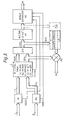
- a received radio signal which may be modulated in the form of am, fm, pm or ssbm is amplified in a radio frequency amplifier RFA and then fed into mixers Ml and M2 in first and second signal paths 1 and 2 respectively.
- the radio signals are mixed with a local oscillator frequency from oscillator LO.
- the local oscillator frequency is set to a frequency defined as the main transmission frequency of the radio signals. For fm, am and pm this is the carrier frequency but for ssbm it is the side band centre frequency.
- the local oscillator frequency is mixed directly with the radio signals but for channel 2, the local oscillator output is phase shifted, preferably through 90° in phase shifted PS, prior.to the mixing. Variations either side of 90° tend to cause deterioration in audio quality unless corrected but do prpvide an operative system. A 90° shift will be assumed for the description and analysis of the system.
- phase shifter PS2 for the radio frequency in path 2.
- the mixed outputs incorporate baseband signals defined as I and Q in channels 1 and 2 respectively and these are in quadrature with respect to each other.
- the quadrature signals are passed through low pass filters LF1 and LF2, amplified in amplifiers AMP1 and AMP2 and again filtered in wideband noise filters WF1 and WF2. Filters WF1 and WF2 may not be necessary in all circumstances.
- Each of the signals I and Q is converted from analogue to digital form in a conventional manner by means of sample and hold devices SH1 and SH2 and a subsequent analogue to digital converter ADC which converts each successive held voltage level into a digital form.
- the digitised I and Q signals are then available for processing in such a manner as to produce the original modulating signal.
- the digital signal processor is represented as a single block DSP.
- the processed digital signals representing the original modulating signal are converted back to analogue form in a digital to analogue converter DAC which provide an analogue-output of the modulating signal.
- the nature of the digital signal processor depends on the nature of modulation of the radio frequency signal with which the receiver is intended to operate. It is possible for the processor to be capable of demodulating only one of fm, am, pm and ssbm but a particular feature of the invention is that simply by providing for a range of digital operations a multi-mode receiver is produced. For this reason it is envisaged that the whole range of signal processing would normally be provided, but a single-mode or two-mode or three-mode receiver could be provided if required.
- FIG. 2 shows details of the digital signal processor for am, fm, pm and ssbm.
- the first and common stage CON involves a conversion of digital I and Q signals to R and 0 where R is the amplitude of the basic modulating signal and 0 is its phase angle. This stage will be described in greater detail sub- .sequently with reference to Figure 3.
- the 6 signal is a direct digital representation of the modulating signal when the radio signal has been transmitted in phase modulated form and is available at output PMO.
- the amplitude signal R is a direct digital representation of the modulating signal when the radio signal has been transmitted in amplitude modulated form and is available at output AMO.
- the differentiated output, d ⁇ /dt (t represents time) is a digital representation of the modulating signal when the radio signal is in frequency modulated form and is available at output FMO.
- Derivation of the original modulating signal aft ssb modulation requires more digital processing in logic block Ll.
- the relationship between R and 6 and an original ssb modulation signal is that the modulating signal is equal to either R Sin ⁇ or R Cos ⁇ .
- ⁇ is derived by subtracting from ⁇ (or adding to ⁇ ) the phase at the offset frequency, effectively performing a single sideband frequency shift. Subtraction or addition depends on whether the upper or the lower sideband respectively is transmitted. Starting with ⁇ , this has the phase at the offset frequency added or subtracted to derive ⁇ .
- the Cos ⁇ or Sin ⁇ can be derived and the resulting value multiplied by R in a multiplier Ml to derive R Cos ⁇ or R Sin ⁇ . This value appears at output SSBO and represents the modulating signal when ssbm was employed in the transmitted radio signal.
- switching means should also be provided to connect the relevant signal to the digital to analogue converter DAC in Figure 1, depending on the nature of the modulation of the received radio signal.
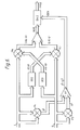
- FIG. 3 is a block diagram of the conversion stage CON of Figure 2, showing greater detail.
- This stage converts the digitised I and Q signals to R and 6 in the following manner.
- Digitised I and Q can have positive and negative values.
- Rectifiers RI and RQ convert I and Q into scaler values
- are fed to a logic block L which first compares the values of
- the logic block L2 has two outputs NUM and DEN which respectively form the numerator and denominator in a divide block DIV.
- are supplied through the logic block L to the outputs NUM and DEN in a manner dependent on the comparison of
- Arctan of the quotient QUO is in the range 0 to 45°.
- the Arctan operation on value QUO is carried out in an Arctan look-up table or by direct calculation in block AT.
- An angle expander AE is fed with the value Arctan QUO and three other bits indicative respectively of the sign of I, the sign of Q and whether
- the latter bit is derived in logic book L.
- This data enables the angle expander to derive a unique value of ⁇ based on Arctan (I/Q) in a 360° range of for example 0° to 360° or - 180° to + 180°.
- the output from the angle expander AE is a digitised value of ⁇ .
- R is always positive (Q and Cos 0 always have the same sign as do I and Sin 8). Thus in deriving R, signs can be ignored.
- R is derived from the same logic operations.
- the output from Arctan block AT can be used and the operation in L3 reduces to deriving 1/Cos X where X is the previously derived Arctan QUO. This possibility is indicated in dotted lines.
- Figure 4 shows a possible addition to the circuit of Figures 1 and 2, which provides for phase control at the phase shifter PS. Phase control or some other form of correction is important for good audio quality.
- the digitised I and Q signals are multiplied together in multiplier M3.
- the product IQ is then filtered in a low pass digital filter DFl.
- the filter output is supplied to a digital to analogue converter DAC 2.
- the output from DAC 2 has a dc level equivalent to the dc level of IQ which is a convenient indication of phase error, i.e. deviation from 90° phase shift in phase shifter PS of Figure 1. This dc level can be applied to phase control input PC in Figure 1 to correct the phase shift to 90°.
- the digital filter DFl is desirable but not essential. Filtering out of higher frequencies derived when multiplying I by Q should not affect the dc level but does simplify the digital to analogue conversion and establishment of the dc level of the output from DAC2.
- Figure 5 shows a further possible addition to the circuit of Figures 1 and 2, to provide balance between the total gain in channel 1 and the total gains in channel 2. This balance is achieved by gain control at the amplifiers AMP1 and AMP2.
- Summing units SUl and SU2 are supplied with
- the two channel gains are equal the sum of
- One sum of n samples is subtracted from the other in subtraction unit S. The resulting difference is (optionally) filtered in low pass digital filter DF2, and converted to analogue form in converter DAC3.
- the dc level of the resulting output is an indication of imbalance in the channels 1 and 2 and is fed to amplifiers AMP1 and AMP2 to correct this gain.
- the digital correction signals for phase and gain derived as described with reference to Figures 4 and 5 may be used as the basis for a calculation of equivalent digital correction value to be applied in the digital processing unit to the digitised I and Q signals.
- Figure 6 shows an alternative technique for deriving the modulating signal from digitised I and Q when the modulation is fm.
- Multipliers M4 and M5 are arranged to produce 1 2 and Q 2 respectively and the latter values are added in addition unit Al to provide I 2 + Q 2 .
- I and Q are each differentiated in digital differentiators DD2 and DD3.
- the resulting dQ/dt is multiplied in multiplier M6 with I to provide I dQ/dt.
- the value Q dI/dt is provided from multiplier M7.
- Outputs from M6 and M7 are subtracted to provide Q dI/dt-I dQ/dt which becomes the numerator for a division unit DIV2.
- the denominator is I 2 + Q 2 , derived previously.
- the output from the division unit D2, which appears at FMO2, is then:
Applications Claiming Priority (2)
| Application Number | Priority Date | Filing Date | Title |
|---|---|---|---|
| GB8127797 | 1981-09-15 | ||
| GB08127797A GB2106734B (en) | 1981-09-15 | 1981-09-15 | Radio receiver |
Publications (3)
| Publication Number | Publication Date |
|---|---|
| EP0074858A2 true EP0074858A2 (fr) | 1983-03-23 |
| EP0074858A3 EP0074858A3 (en) | 1984-09-19 |
| EP0074858B1 EP0074858B1 (fr) | 1987-07-08 |
Family
ID=10524508
Family Applications (1)
| Application Number | Title | Priority Date | Filing Date |
|---|---|---|---|
| EP82304870A Expired EP0074858B1 (fr) | 1981-09-15 | 1982-09-15 | Récepteur radio |
Country Status (5)
| Country | Link |
|---|---|
| US (1) | US4470147A (fr) |
| EP (1) | EP0074858B1 (fr) |
| JP (1) | JPS58114532A (fr) |
| DE (1) | DE3276738D1 (fr) |
| GB (1) | GB2106734B (fr) |
Cited By (13)
| Publication number | Priority date | Publication date | Assignee | Title |
|---|---|---|---|---|
| DE3341430A1 (de) * | 1982-11-12 | 1984-07-19 | Matsushita Electric Industrial Co., Ltd., Kadoma, Osaka | Fs-synchronempfaenger fuer die verwendung als fs-empfaenger und als vtr-videotuner |
| EP0143539A2 (fr) * | 1983-10-29 | 1985-06-05 | Stc Plc | Circuit numérique de démodulation pour deux signaux (I,Q) en quadratures |
| EP0169915A1 (fr) * | 1984-06-06 | 1986-02-05 | Deutsche ITT Industries GmbH | Démodulateur de phase numérique |
| EP0180339A2 (fr) * | 1984-10-25 | 1986-05-07 | Stc Plc | Emetteur-récepteur radio multimode |
| EP0186568A2 (fr) * | 1984-12-17 | 1986-07-02 | Fairchild Weston Systems Inc. | Démodulateur numérique pour des signaux modulés de façon continue en phase ou en fréquence |
| EP0208915A1 (fr) * | 1985-07-19 | 1987-01-21 | ANT Nachrichtentechnik GmbH | Procédé de démodulation d'un signal modulé en déplacement de fréquence et de phase |
| FR2595895A1 (fr) * | 1986-03-13 | 1987-09-18 | France Etat | Double demodulateur numerique |
| EP0255175A2 (fr) * | 1986-08-01 | 1988-02-03 | Philips Electronics Uk Limited | Démodulation d'un signal modulé angulairement |
| EP0343273A1 (fr) * | 1988-05-27 | 1989-11-29 | Deutsche ITT Industries GmbH | Circuit de correction pour une paire de signaux numériques en quadrature |
| GB2219899A (en) * | 1988-06-17 | 1989-12-20 | Philips Electronic Associated | A zero if receiver |
| EP0235264A4 (fr) * | 1985-09-03 | 1990-02-26 | Motorola Inc | Recepteur de frequence radio numerique. |
| DE3938643A1 (de) * | 1988-11-22 | 1990-05-23 | Ascom Radiocom Ag | Verfahren zum rekonstruieren verlorener dc-nutzanteile an zf-signalen in einem direct-conversion-empfaenger und empfaenger zum durchfuehren des verfahrens |
| WO2002089311A2 (fr) * | 2001-04-27 | 2002-11-07 | Infineon Technologies Ag | Recepteur haute frequence |
Families Citing this family (34)
| Publication number | Priority date | Publication date | Assignee | Title |
|---|---|---|---|---|
| US4675614A (en) * | 1982-10-20 | 1987-06-23 | Rockwell International Corporation | Phase difference measurement system |
| JPS5980048A (ja) * | 1982-10-30 | 1984-05-09 | Nec Corp | 自動位相調整回路 |
| US4608540A (en) * | 1983-07-04 | 1986-08-26 | Clarion Co., Ltd. | Phase-shift keying demodulator |
| JPS60183862A (ja) * | 1984-03-02 | 1985-09-19 | Toshiba Corp | デイジタル信号処理回路 |
| US4731796A (en) * | 1984-10-25 | 1988-03-15 | Stc, Plc | Multi-mode radio transceiver |
| GB2172159A (en) * | 1985-03-07 | 1986-09-10 | Stc Plc | A/d converters |
| DE3613994A1 (de) * | 1986-04-25 | 1987-10-29 | Schrack Elektronik Ag | Schaltungsanordnung zum demodulieren frequenzmodulierter signale |
| GB2192506B (en) * | 1986-07-12 | 1990-05-30 | Stc Plc | Demodulation circuit |
| US4811425A (en) * | 1987-01-09 | 1989-03-07 | Itt Avionics, A Division Of Itt Corporation | Apparatus for reducing the effects of local oscillator leakage in mixers employed in zero IF receivers |
| US4933958A (en) * | 1987-12-17 | 1990-06-12 | Siemens Aktiengesellschaft | Method for receiving carrier oscillations modulated with a useful signal |
| US4853944A (en) * | 1988-03-10 | 1989-08-01 | Allied-Signal Inc. | Digital AM/FM/φM demodulator |
| GB2215945A (en) * | 1988-03-26 | 1989-09-27 | Stc Plc | Digital direct conversion radio |
| GB2220315A (en) * | 1988-07-01 | 1990-01-04 | Philips Electronic Associated | Signal amplitude-determining apparatus |
| CH676405A5 (fr) * | 1988-11-22 | 1991-01-15 | Ascom Radiocom Ag | |
| JPH0474230U (fr) * | 1990-11-09 | 1992-06-29 | ||
| GB9408759D0 (en) * | 1994-05-03 | 1994-06-22 | Texas Instruments Ltd | Using high level cad tools to design application specific standard products for tv sound decoder systems |
| DE19608451A1 (de) * | 1996-03-05 | 1997-09-11 | Philips Patentverwaltung | Verfahren zum Übertragen von Informationen |
| US6016304A (en) * | 1996-08-07 | 2000-01-18 | Raytheon Company | RF phase and/or amplitude control device |
| SE508290C2 (sv) * | 1997-01-21 | 1998-09-21 | Ericsson Telefon Ab L M | Mottagaranordning för två frekvensband |
| JP4294114B2 (ja) * | 1998-03-02 | 2009-07-08 | パイオニア株式会社 | ディジタルfm検波回路 |
| US6256358B1 (en) * | 1998-03-27 | 2001-07-03 | Visteon Global Technologies, Inc. | Digital signal processing architecture for multi-band radio receiver |
| DE19921921A1 (de) * | 1999-05-12 | 2000-11-16 | Bosch Gmbh Robert | Einseitenbandmischer |
| CA2281236C (fr) | 1999-09-01 | 2010-02-09 | Tajinder Manku | Methodes rf de conversion directe au moyen d'un signal virtuel d'oscillateur local |
| WO2002082673A1 (fr) * | 2001-04-05 | 2002-10-17 | Koninklijke Philips Electronics N.V. | Recepteur de frequence radio |
| US20040082304A1 (en) * | 2002-10-24 | 2004-04-29 | Gehring Mark R. | Demodulator architecture and associated methods |
| US7123892B2 (en) * | 2003-10-10 | 2006-10-17 | Freescale Semiconductor, Inc. | Architecture for an AM/FM digital intermediate frequency radio |
| US20050191986A1 (en) * | 2004-02-27 | 2005-09-01 | Lin Hung C. | FM detector for direct-conversion receiver |
| US7609784B1 (en) | 2004-04-26 | 2009-10-27 | Dgi Creations, Llc | Signal decoding method and apparatus with dynamic noise threshold |
| US7242729B1 (en) | 2004-04-26 | 2007-07-10 | Dgi Creations, Llc | Signal decoding method and apparatus |
| FR2878667B1 (fr) * | 2004-11-29 | 2007-08-24 | Eads Telecom Soc Par Actions S | Procede et dispositif de conversion analogique numerique avec correction de dissymetrie |
| US20060242220A1 (en) * | 2005-04-20 | 2006-10-26 | Texas Instruments, Inc. | Hardware divider |
| US20060276239A1 (en) * | 2005-06-02 | 2006-12-07 | Lam Man L | Direct conversion radio station operable pursuant to a coded squelch scheme and associated method |
| US7650084B2 (en) * | 2005-09-27 | 2010-01-19 | Alcatel-Lucent Usa Inc. | Optical heterodyne receiver and method of extracting data from a phase-modulated input optical signal |
| WO2015067987A1 (fr) * | 2013-11-05 | 2015-05-14 | Eutelsat S A | Système d'émission et de réception de signaux radiofréquences portant des modes harmoniques complexes |
Citations (2)
| Publication number | Priority date | Publication date | Assignee | Title |
|---|---|---|---|---|
| US4090145A (en) * | 1969-03-24 | 1978-05-16 | Webb Joseph A | Digital quadrature demodulator |
| GB2040615A (en) * | 1979-01-26 | 1980-08-28 | Licentia Gmbh | Receiver system |
Family Cites Families (6)
| Publication number | Priority date | Publication date | Assignee | Title |
|---|---|---|---|---|
| US3426281A (en) * | 1966-02-28 | 1969-02-04 | Us Army | Reception of time dispersed signals utilizing impulse response storage in recirculating delay lines |
| US3646448A (en) * | 1970-02-16 | 1972-02-29 | Datamax Corp | Quadrature injection control circuit |
| US3669511A (en) * | 1970-09-17 | 1972-06-13 | North American Rockwell | System for phase locking on a virtual carrier received by an asymmetrical receiver |
| US3787775A (en) * | 1973-03-28 | 1974-01-22 | Trw Inc | Phase correction circuit |
| US4004226A (en) * | 1975-07-23 | 1977-01-18 | Codex Corporation | QAM receiver having automatic adaptive equalizer |
| DE3114063A1 (de) * | 1981-04-07 | 1982-10-21 | Licentia Patent-Verwaltungs-Gmbh, 6000 Frankfurt | Empfangssystem |
-
1981
- 1981-09-15 GB GB08127797A patent/GB2106734B/en not_active Expired
-
1982
- 1982-09-08 US US06/415,968 patent/US4470147A/en not_active Expired - Lifetime
- 1982-09-14 JP JP57159057A patent/JPS58114532A/ja active Granted
- 1982-09-15 EP EP82304870A patent/EP0074858B1/fr not_active Expired
- 1982-09-15 DE DE8282304870T patent/DE3276738D1/de not_active Expired
Patent Citations (2)
| Publication number | Priority date | Publication date | Assignee | Title |
|---|---|---|---|---|
| US4090145A (en) * | 1969-03-24 | 1978-05-16 | Webb Joseph A | Digital quadrature demodulator |
| GB2040615A (en) * | 1979-01-26 | 1980-08-28 | Licentia Gmbh | Receiver system |
Cited By (25)
| Publication number | Priority date | Publication date | Assignee | Title |
|---|---|---|---|---|
| DE3341430A1 (de) * | 1982-11-12 | 1984-07-19 | Matsushita Electric Industrial Co., Ltd., Kadoma, Osaka | Fs-synchronempfaenger fuer die verwendung als fs-empfaenger und als vtr-videotuner |
| EP0143539A2 (fr) * | 1983-10-29 | 1985-06-05 | Stc Plc | Circuit numérique de démodulation pour deux signaux (I,Q) en quadratures |
| EP0143539A3 (fr) * | 1983-10-29 | 1987-06-24 | Stc Plc | Circuit numérique de démodulation pour deux signaux (I,Q) en quadratures |
| EP0169915A1 (fr) * | 1984-06-06 | 1986-02-05 | Deutsche ITT Industries GmbH | Démodulateur de phase numérique |
| EP0180339A2 (fr) * | 1984-10-25 | 1986-05-07 | Stc Plc | Emetteur-récepteur radio multimode |
| EP0180339A3 (fr) * | 1984-10-25 | 1988-01-07 | Stc Plc | Emetteur-récepteur radio multimode |
| EP0186568A3 (fr) * | 1984-12-17 | 1988-01-27 | Fairchild Weston Systems Inc. | Démodulateur numérique pour des signaux modulés de façon continue en phase ou en fréquence |
| EP0186568A2 (fr) * | 1984-12-17 | 1986-07-02 | Fairchild Weston Systems Inc. | Démodulateur numérique pour des signaux modulés de façon continue en phase ou en fréquence |
| EP0208915A1 (fr) * | 1985-07-19 | 1987-01-21 | ANT Nachrichtentechnik GmbH | Procédé de démodulation d'un signal modulé en déplacement de fréquence et de phase |
| EP0235264A4 (fr) * | 1985-09-03 | 1990-02-26 | Motorola Inc | Recepteur de frequence radio numerique. |
| US4804924A (en) * | 1986-03-13 | 1989-02-14 | L'etat Francais Represente Par Le Ministre Des Ptt (Cnet) | Digital double demodulator |
| FR2595895A1 (fr) * | 1986-03-13 | 1987-09-18 | France Etat | Double demodulateur numerique |
| WO1987005758A1 (fr) * | 1986-03-13 | 1987-09-24 | ETAT FRANCAIS représenté par LE MINISTRE DES PTT ( | Double demodulateur numerique |
| EP0255175A3 (fr) * | 1986-08-01 | 1989-03-15 | Philips Electronics Uk Limited | Démodulation d'un signal modulé angulairement |
| EP0255175A2 (fr) * | 1986-08-01 | 1988-02-03 | Philips Electronics Uk Limited | Démodulation d'un signal modulé angulairement |
| EP0343273A1 (fr) * | 1988-05-27 | 1989-11-29 | Deutsche ITT Industries GmbH | Circuit de correction pour une paire de signaux numériques en quadrature |
| US4926443A (en) * | 1988-05-27 | 1990-05-15 | Deutsche Itt Industries Gmbh | Correction circuit for a digital quadrature-signal pair |
| EP0346986A2 (fr) * | 1988-06-17 | 1989-12-20 | Philips Electronics Uk Limited | Récepteur à fréquence intermédiaire zéro |
| GB2219899A (en) * | 1988-06-17 | 1989-12-20 | Philips Electronic Associated | A zero if receiver |
| EP0346986A3 (fr) * | 1988-06-17 | 1992-04-22 | Philips Electronics Uk Limited | Récepteur à fréquence intermédiaire zéro |
| US5159710A (en) * | 1988-06-17 | 1992-10-27 | U.S. Philips Corp. | Zero IF receiver employing, in quadrature related signal paths, amplifiers having substantially sinh-1 transfer characteristics |
| DE3938643A1 (de) * | 1988-11-22 | 1990-05-23 | Ascom Radiocom Ag | Verfahren zum rekonstruieren verlorener dc-nutzanteile an zf-signalen in einem direct-conversion-empfaenger und empfaenger zum durchfuehren des verfahrens |
| DE3938643C2 (de) * | 1988-11-22 | 1999-03-25 | Motorola Inc | Verfahren zum Rekonstruieren abgetrennter Gleichspannungsnutzanteile an ZF-Signalen in einem Direct-Conversion-Empfänger und Empfänger zum Durchführen des Verfahrens |
| WO2002089311A2 (fr) * | 2001-04-27 | 2002-11-07 | Infineon Technologies Ag | Recepteur haute frequence |
| WO2002089311A3 (fr) * | 2001-04-27 | 2003-11-20 | Infineon Technologies Ag | Recepteur haute frequence |
Also Published As
| Publication number | Publication date |
|---|---|
| DE3276738D1 (en) | 1987-08-13 |
| US4470147A (en) | 1984-09-04 |
| GB2106734B (en) | 1986-01-15 |
| EP0074858B1 (fr) | 1987-07-08 |
| EP0074858A3 (en) | 1984-09-19 |
| JPS58114532A (ja) | 1983-07-07 |
| GB2106734A (en) | 1983-04-13 |
| JPS6412128B2 (fr) | 1989-02-28 |
Similar Documents
| Publication | Publication Date | Title |
|---|---|---|
| US4470147A (en) | Radio receiver with quadrature demodulation and digital processing | |
| US6073001A (en) | Down conversion mixer | |
| EP0691057B1 (fr) | Circuit modulateur de phase tetravalente de signal i/q | |
| US5719527A (en) | Method and apparatus for amplifying, modulating and demodulating | |
| JP4355443B2 (ja) | 2重デジタル低if複合受信機 | |
| US4476585A (en) | Baseband demodulator for FM signals | |
| JPH0690261A (ja) | 直接変換受信機における信号チャネル間の利得及び位相エラー制御方法及び装置 | |
| US7492838B2 (en) | Apparatus for compensating for phase mismatch in QPSK demodulator | |
| GB2094079A (en) | Fm demodulator | |
| US6356594B1 (en) | Data converter | |
| US4599743A (en) | Baseband demodulator for FM and/or AM signals | |
| US5339040A (en) | AM demodulation receiver using digital signal processor | |
| US4677690A (en) | Baseband demodulator for FM and/or AM signals | |
| US5638401A (en) | Method and apparatus for generating plural quadrature modulated carriers | |
| JP3386114B2 (ja) | 復調装置及び方法 | |
| GB2213006A (en) | Zero-IF transmitter with error correction | |
| US20010041546A1 (en) | Direct-conversion modulation with reduced local oscillator leakage | |
| GB2236225A (en) | Superhetorodyne circuit | |
| US20030228860A1 (en) | Integrated radio-frequency receiver | |
| US5081650A (en) | Data receiver | |
| US7409008B2 (en) | Transmitting arrangement for mobile radio | |
| KR20010048190A (ko) | 수신기 | |
| US7209723B2 (en) | Direct conversion circuit having reduced bit errors | |
| EP0721270A1 (fr) | Récepteur à conversion directe pour signaux FSK multiniveaux | |
| KR20010041140A (ko) | 무선 주파수 신호의 전송 회로, 무선전화 장치 및 주파수변환기 |
Legal Events
| Date | Code | Title | Description |
|---|---|---|---|
| PUAI | Public reference made under article 153(3) epc to a published international application that has entered the european phase |
Free format text: ORIGINAL CODE: 0009012 |
|
| AK | Designated contracting states |
Designated state(s): CH DE LI SE |
|
| PUAL | Search report despatched |
Free format text: ORIGINAL CODE: 0009013 |
|
| AK | Designated contracting states |
Designated state(s): CH DE LI SE |
|
| 17P | Request for examination filed |
Effective date: 19840817 |
|
| GRAA | (expected) grant |
Free format text: ORIGINAL CODE: 0009210 |
|
| AK | Designated contracting states |
Kind code of ref document: B1 Designated state(s): CH DE LI SE |
|
| REF | Corresponds to: |
Ref document number: 3276738 Country of ref document: DE Date of ref document: 19870813 |
|
| PLBE | No opposition filed within time limit |
Free format text: ORIGINAL CODE: 0009261 |
|
| STAA | Information on the status of an ep patent application or granted ep patent |
Free format text: STATUS: NO OPPOSITION FILED WITHIN TIME LIMIT |
|
| PG25 | Lapsed in a contracting state [announced via postgrant information from national office to epo] |
Ref country code: DE Effective date: 19880601 |
|
| 26N | No opposition filed | ||
| PG25 | Lapsed in a contracting state [announced via postgrant information from national office to epo] |
Ref country code: SE Effective date: 19880916 |
|
| PG25 | Lapsed in a contracting state [announced via postgrant information from national office to epo] |
Ref country code: LI Effective date: 19880930 Ref country code: CH Effective date: 19880930 |
|
| REG | Reference to a national code |
Ref country code: CH Ref legal event code: PL |
|
| EUG | Se: european patent has lapsed |
Ref document number: 82304870.7 Effective date: 19890712 |