EP0072673A2 - Verdrahtungsträgerfolie für die elektrische Verbindung zwischen elektronischen Bauelementen und einer externen Schaltung - Google Patents
Verdrahtungsträgerfolie für die elektrische Verbindung zwischen elektronischen Bauelementen und einer externen Schaltung Download PDFInfo
- Publication number
- EP0072673A2 EP0072673A2 EP82304271A EP82304271A EP0072673A2 EP 0072673 A2 EP0072673 A2 EP 0072673A2 EP 82304271 A EP82304271 A EP 82304271A EP 82304271 A EP82304271 A EP 82304271A EP 0072673 A2 EP0072673 A2 EP 0072673A2
- Authority
- EP
- European Patent Office
- Prior art keywords
- terminals
- array
- tape
- external
- internal
- Prior art date
- Legal status (The legal status is an assumption and is not a legal conclusion. Google has not performed a legal analysis and makes no representation as to the accuracy of the status listed.)
- Granted
Links
- 238000000034 method Methods 0.000 claims description 17
- 238000012360 testing method Methods 0.000 claims description 14
- 229910052751 metal Inorganic materials 0.000 claims description 9
- 239000002184 metal Substances 0.000 claims description 9
- 239000004642 Polyimide Substances 0.000 claims description 3
- 239000011810 insulating material Substances 0.000 claims description 3
- 229920001721 polyimide Polymers 0.000 claims description 3
- 239000007787 solid Substances 0.000 claims description 3
- 150000003839 salts Chemical class 0.000 claims 1
- 238000003491 array Methods 0.000 abstract description 5
- 239000010410 layer Substances 0.000 description 29
- 239000004065 semiconductor Substances 0.000 description 16
- 229920002120 photoresistant polymer Polymers 0.000 description 14
- 239000000463 material Substances 0.000 description 7
- RYGMFSIKBFXOCR-UHFFFAOYSA-N Copper Chemical compound [Cu] RYGMFSIKBFXOCR-UHFFFAOYSA-N 0.000 description 6
- 229910052802 copper Inorganic materials 0.000 description 6
- 239000010949 copper Substances 0.000 description 6
- 239000010408 film Substances 0.000 description 6
- 239000000919 ceramic Substances 0.000 description 5
- PXHVJJICTQNCMI-UHFFFAOYSA-N Nickel Chemical compound [Ni] PXHVJJICTQNCMI-UHFFFAOYSA-N 0.000 description 4
- 238000005530 etching Methods 0.000 description 4
- 239000000758 substrate Substances 0.000 description 4
- 239000011104 metalized film Substances 0.000 description 3
- 150000002739 metals Chemical class 0.000 description 3
- 229920005575 poly(amic acid) Polymers 0.000 description 3
- ATJFFYVFTNAWJD-UHFFFAOYSA-N Tin Chemical compound [Sn] ATJFFYVFTNAWJD-UHFFFAOYSA-N 0.000 description 2
- 239000004020 conductor Substances 0.000 description 2
- 238000013461 design Methods 0.000 description 2
- 239000003989 dielectric material Substances 0.000 description 2
- 238000005553 drilling Methods 0.000 description 2
- 239000011888 foil Substances 0.000 description 2
- PCHJSUWPFVWCPO-UHFFFAOYSA-N gold Chemical compound [Au] PCHJSUWPFVWCPO-UHFFFAOYSA-N 0.000 description 2
- 229910052737 gold Inorganic materials 0.000 description 2
- 239000010931 gold Substances 0.000 description 2
- 238000003384 imaging method Methods 0.000 description 2
- 238000004519 manufacturing process Methods 0.000 description 2
- 229910052759 nickel Inorganic materials 0.000 description 2
- 230000002093 peripheral effect Effects 0.000 description 2
- 238000001020 plasma etching Methods 0.000 description 2
- 238000007747 plating Methods 0.000 description 2
- 230000005855 radiation Effects 0.000 description 2
- 238000005476 soldering Methods 0.000 description 2
- 238000005382 thermal cycling Methods 0.000 description 2
- 229910052718 tin Inorganic materials 0.000 description 2
- 239000011135 tin Substances 0.000 description 2
- 239000004952 Polyamide Substances 0.000 description 1
- BQCADISMDOOEFD-UHFFFAOYSA-N Silver Chemical compound [Ag] BQCADISMDOOEFD-UHFFFAOYSA-N 0.000 description 1
- 239000002253 acid Substances 0.000 description 1
- NIXOWILDQLNWCW-UHFFFAOYSA-N acrylic acid group Chemical group C(C=C)(=O)O NIXOWILDQLNWCW-UHFFFAOYSA-N 0.000 description 1
- 230000003213 activating effect Effects 0.000 description 1
- 229910045601 alloy Inorganic materials 0.000 description 1
- 239000000956 alloy Substances 0.000 description 1
- 229910052782 aluminium Inorganic materials 0.000 description 1
- XAGFODPZIPBFFR-UHFFFAOYSA-N aluminium Chemical compound [Al] XAGFODPZIPBFFR-UHFFFAOYSA-N 0.000 description 1
- PNEYBMLMFCGWSK-UHFFFAOYSA-N aluminium oxide Inorganic materials [O-2].[O-2].[O-2].[Al+3].[Al+3] PNEYBMLMFCGWSK-UHFFFAOYSA-N 0.000 description 1
- 239000003637 basic solution Substances 0.000 description 1
- 239000011248 coating agent Substances 0.000 description 1
- 238000000576 coating method Methods 0.000 description 1
- 238000007906 compression Methods 0.000 description 1
- 238000010276 construction Methods 0.000 description 1
- 239000000356 contaminant Substances 0.000 description 1
- 238000007796 conventional method Methods 0.000 description 1
- 238000005520 cutting process Methods 0.000 description 1
- 230000006735 deficit Effects 0.000 description 1
- 238000004070 electrodeposition Methods 0.000 description 1
- 238000007772 electroless plating Methods 0.000 description 1
- 238000010894 electron beam technology Methods 0.000 description 1
- NBVXSUQYWXRMNV-UHFFFAOYSA-N fluoromethane Chemical compound FC NBVXSUQYWXRMNV-UHFFFAOYSA-N 0.000 description 1
- 239000003365 glass fiber Substances 0.000 description 1
- 238000011065 in-situ storage Methods 0.000 description 1
- 238000003801 milling Methods 0.000 description 1
- 239000002245 particle Substances 0.000 description 1
- -1 poly(imide-amide) Polymers 0.000 description 1
- 229920003223 poly(pyromellitimide-1,4-diphenyl ether) Polymers 0.000 description 1
- 229920002492 poly(sulfone) Polymers 0.000 description 1
- 229920002647 polyamide Polymers 0.000 description 1
- 229920000728 polyester Polymers 0.000 description 1
- 229920001296 polysiloxane Polymers 0.000 description 1
- 238000012545 processing Methods 0.000 description 1
- 229910052710 silicon Inorganic materials 0.000 description 1
- 239000010703 silicon Substances 0.000 description 1
- 229910052709 silver Inorganic materials 0.000 description 1
- 239000004332 silver Substances 0.000 description 1
- 239000002356 single layer Substances 0.000 description 1
- 229910000679 solder Inorganic materials 0.000 description 1
- 239000000243 solution Substances 0.000 description 1
- 239000002904 solvent Substances 0.000 description 1
- 238000000992 sputter etching Methods 0.000 description 1
- 239000000126 substance Substances 0.000 description 1
- 229920001187 thermosetting polymer Polymers 0.000 description 1
- 239000010409 thin film Substances 0.000 description 1
- 238000012546 transfer Methods 0.000 description 1
Images


Classifications
-
- H—ELECTRICITY
- H01—ELECTRIC ELEMENTS
- H01L—SEMICONDUCTOR DEVICES NOT COVERED BY CLASS H10
- H01L22/00—Testing or measuring during manufacture or treatment; Reliability measurements, i.e. testing of parts without further processing to modify the parts as such; Structural arrangements therefor
- H01L22/30—Structural arrangements specially adapted for testing or measuring during manufacture or treatment, or specially adapted for reliability measurements
- H01L22/32—Additional lead-in metallisation on a device or substrate, e.g. additional pads or pad portions, lines in the scribe line, sacrificed conductors
-
- H—ELECTRICITY
- H01—ELECTRIC ELEMENTS
- H01L—SEMICONDUCTOR DEVICES NOT COVERED BY CLASS H10
- H01L23/00—Details of semiconductor or other solid state devices
- H01L23/12—Mountings, e.g. non-detachable insulating substrates
- H01L23/14—Mountings, e.g. non-detachable insulating substrates characterised by the material or its electrical properties
- H01L23/145—Organic substrates, e.g. plastic
-
- H—ELECTRICITY
- H01—ELECTRIC ELEMENTS
- H01L—SEMICONDUCTOR DEVICES NOT COVERED BY CLASS H10
- H01L23/00—Details of semiconductor or other solid state devices
- H01L23/48—Arrangements for conducting electric current to or from the solid state body in operation, e.g. leads, terminal arrangements ; Selection of materials therefor
- H01L23/488—Arrangements for conducting electric current to or from the solid state body in operation, e.g. leads, terminal arrangements ; Selection of materials therefor consisting of soldered or bonded constructions
- H01L23/498—Leads, i.e. metallisations or lead-frames on insulating substrates, e.g. chip carriers
- H01L23/4985—Flexible insulating substrates
-
- H—ELECTRICITY
- H01—ELECTRIC ELEMENTS
- H01L—SEMICONDUCTOR DEVICES NOT COVERED BY CLASS H10
- H01L24/00—Arrangements for connecting or disconnecting semiconductor or solid-state bodies; Methods or apparatus related thereto
- H01L24/01—Means for bonding being attached to, or being formed on, the surface to be connected, e.g. chip-to-package, die-attach, "first-level" interconnects; Manufacturing methods related thereto
- H01L24/50—Tape automated bonding [TAB] connectors, i.e. film carriers; Manufacturing methods related thereto
-
- H—ELECTRICITY
- H01—ELECTRIC ELEMENTS
- H01L—SEMICONDUCTOR DEVICES NOT COVERED BY CLASS H10
- H01L24/00—Arrangements for connecting or disconnecting semiconductor or solid-state bodies; Methods or apparatus related thereto
- H01L24/80—Methods for connecting semiconductor or other solid state bodies using means for bonding being attached to, or being formed on, the surface to be connected
- H01L24/86—Methods for connecting semiconductor or other solid state bodies using means for bonding being attached to, or being formed on, the surface to be connected using tape automated bonding [TAB]
-
- H—ELECTRICITY
- H01—ELECTRIC ELEMENTS
- H01L—SEMICONDUCTOR DEVICES NOT COVERED BY CLASS H10
- H01L2924/00—Indexing scheme for arrangements or methods for connecting or disconnecting semiconductor or solid-state bodies as covered by H01L24/00
- H01L2924/10—Details of semiconductor or other solid state devices to be connected
- H01L2924/11—Device type
- H01L2924/12—Passive devices, e.g. 2 terminal devices
- H01L2924/1204—Optical Diode
- H01L2924/12042—LASER
-
- Y—GENERAL TAGGING OF NEW TECHNOLOGICAL DEVELOPMENTS; GENERAL TAGGING OF CROSS-SECTIONAL TECHNOLOGIES SPANNING OVER SEVERAL SECTIONS OF THE IPC; TECHNICAL SUBJECTS COVERED BY FORMER USPC CROSS-REFERENCE ART COLLECTIONS [XRACs] AND DIGESTS
- Y10—TECHNICAL SUBJECTS COVERED BY FORMER USPC
- Y10T—TECHNICAL SUBJECTS COVERED BY FORMER US CLASSIFICATION
- Y10T29/00—Metal working
- Y10T29/49—Method of mechanical manufacture
- Y10T29/49002—Electrical device making
- Y10T29/49117—Conductor or circuit manufacturing
- Y10T29/49124—On flat or curved insulated base, e.g., printed circuit, etc.
- Y10T29/4913—Assembling to base an electrical component, e.g., capacitor, etc.
- Y10T29/49144—Assembling to base an electrical component, e.g., capacitor, etc. by metal fusion
Definitions
- This invention is directed to articles and methods useful in electrically interconnecting electronic components. More particularly it is directed to flexible tape constructions having a flexible electrically insulating body, and arrays of internal and external terminals in said body which are electrically interconnected by a multiplicity of conductive paths. The paths are provided in more than one level so as to make maximum use of the available space for the internal and external terminals. At least some of the conductive paths are essentially completely embedded or buried within the body.
- the tape is particularly useful in electrically connecting small electronic components, such as semiconductor chips, to external circuitry, such as ceramic packages.
- Small electronic components such as semiconductor chips or devices
- Devices employing peripheral bonding locations provide only a limited number of access points for electrical connection due to the small area available for such points.
- Devices employing an array of contact points also known as "flip chip” devices) overcome this disadvantage by increasing the area available for such points.
- Flip chip devices are commonly electrically interconnected to external circuitry by aligning its array of bonding locations, such as metallized bumps, with corresponding bonding locations on the external circuitry and forming a metallurgical bond between the two sets of bonding locations by, for example, reflow soldering, thermocompression bonding, or ultrasonic bonding.
- the contact area is limited to the area of the metallurgical bonds. This can be as small as 5% of the area of the device and can cause a severe impairment of removal of heat from the device to the substrate.
- the present invention overcomes these disadvantages. It provides a compliant or flexible article which can absorb the stress caused by thermal expansion mismatch. As a result, the bonding locations may be located anywhere on the face of the semiconductor device rather than only in an array of limited size. As a result, more electrical connection points may be provided on a semiconductor device.
- the present invention also permits one surface of the device to be placed in maximum contact with the substrate while the bonding locations on the other surface of the device can be placed in thermal contact with the tape, thereby permitting maximum thermal transfer.
- the present invention permits direct electrical contact to the back of the device if desired. This is particularly useful when it is desired to electrically ground the device.
- the present invention provides still another advantage.
- the present invention when applied to the electronic component and the external circuitry it protects the assembled device from alpha particles which would otherwise impinge upon the electronic component and undesirably change its electrical state.
- U.S. Patent 3,832,769 and 3,868,724 disclose structures wherein a pattern of electrical contacts on one surface are electrically interconnected to a pattern of electrical contacts on another surface. These structures employ only single layers of a dielectric material and a conductive material to join the two patterns of electrical contacts. This type of structure provides only limited space for electrical contact points.
- U.S. Patent 4,064,552 describes a tape bearing a foil pattern thereon which has individual electrical terminals to receive components.
- the foil pattern is on a dielectric carrier and has interlayered connections through apertures in the carrier.
- the dielectric layers of the tape are adhesively secured to one another.
- U.S. Patent 3,780,352 discloses a structure wherein a set of thin metallic film strips are bonded to a thin flexible dielectric support. The metal strips interconnect the contact pads on semiconductor chips and selected leads to electrically interconnect the semiconductor device and the leads.
- U.S. Patent 4,251,852 discloses a wiring skirt for electrically interconnecting two identical semiconductor chips to a common set of contacts.
- the wiring skirt is built in-situ around the semiconductor chips.
- the present invention provides a flexible area-bonding tape for providing electrical interconnections between electronic components and external circuitry.
- the tape comprises a flexible, solid, electrically insulating body having a predetermined array of internal terminals for electrical interconnection to the electrical components and a predetermined array of external terminals for electrical interconnection to the external circuitry.
- the internal and external terminals are electrically interconnected by a multiplicity of conductive paths provided in more than one layer, at least some of which are completely embedded or buried within the body.
- the tape of the invention is comprised of multiple, alternate layers of an electrical conductor, and an insulating body.
- the electrically conductive paths are comprised of discrete electrically conductive traces of a desired geometry so as to interconnect the individual terminals of the array of internal terminals to desired terminals of the d rray of external terminals.
- the material of the insulating body separates the various conductive traces and contains holes or vias which permit the traces to be routed in a number of ways so as to provide the maximum latitude in the design of the various arrays of terminals.
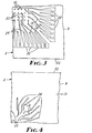
- conductive paths 14 are at least partially electrically isolated from one another and are situated on layer 9 of the body of the tape 2. Conductive paths 14 are present on both sides of layer 9.
- FIGURE 3 shows a pattern of conductive paths 14 as it might exist between layers 8 and 9 of tape 2 while FIGURE 4 shows a pattern of conductive paths 14 as it would exist on top surface 13 of layer 9, which corresponds to the top surface of tape 2.
- Ends 24 of conductive paths 14 are electrically connected to external terminals 11 at certain of vias 15 and 26 in layers 9 and 8 while ends 25 of conductive paths 14 are electrically connected to internal terminals 10 at other of vias 15 and 26. See FIGURE 10.
- the arrays of internal, external, and optional test terminals, and the geometric configuration of conductive paths 14 are selected so as to achieve a desired pattern of land areas. While the exact configuration of the terminals and paths is not critical to the invention, they must be selected so as to correspond to those required for interconnection to the electronic component and the external circuitry, and so as to avoid any undesired electrical interconnections, that is short-circuiting. Within these parameters then, a wide variety of designs and configurations may be utilized.
- the insulating material of layers 8 and 9 is flexible and is preferably in the range of 2.5-250 microns in thickness.
- Useful insulating materials include thin, flexible films of polyimide, polyester, acrylic, fluorocarbon, polysulfone, polyamide, poly(imide-amide), silicone, and glass fiber reinforced thermoset plastics.
- the various terminals and conductive paths utilized in the tape are preferably metals such as aluminum, copper, nickel, silver, gold, tin and the like. Alloys of these metals either with each other or with other metals are also useful. Bimetal terminals, for example solder plated copper, tin plated copper or gold plated nickel, are also useful.
- the thickness of the various terminals and paths must be at least sufficient to allow electrical conductivity and they may be as thick as 125 microns, although thinner terminals and paths, such as 10 to 15 microns, are generally preferred for reasons of economics.
- the various terminals utilized throughout the tape 2 may have any geometric shape and dimension desired. Thus, for example, they may be circular, rectangular, triangular, etc. Generally the terminals in a given array are all of the same dimensions. although they need not be so. Thus, for example, circular terminals may have diameters of from 25 to 500 microns. Terminals of other shapes will commonly have surface areas corresponding to those of the circular terminals. Additionally, the terminals may comprise raised areas which extend beyond bottom surface 21 of tape 2 or, alternatively, they may comprise recessed areas as are shown in FIGURE 10.
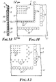
- the array of internal terminals 10 may comprise a multiplicity of horizontal and vertical rows of metal land areas as is shown in FIGURES 2-4, 11, and 13. This array is of course merely descriptive and may be varied to suit the pattern of the bonding locations of the electronic component to which it is to be attached.
- the array of external terminals 11 is preferably peripherally situated about the array of internal terminals 10. It may comprise a single row of terminals which surrounds the array of internal terminals 10 as is shown in FIGURES 2-4 and 11, or it may comprise a double row of terminals as is shown in FIGURE 13. Again, the exact pattern of the array of external terminals 11 may be varied to meet the pattern of the bonding locations of the external circuitry to which it is to be attached. It is not necessary that the array of external terminals 11 totally surround the array of internal terminals 10.
- the array of test terminals 20 may also vary in its pattern.
- FIGURES show the array as a row of land areas which surrounds the array of external terminals 11 other patterns may be utilized if desired.
- FIGURES 11 and 12 show an alternative embodiment of the present invention wherein a portion of the flexible insulating body, here layers 8 and 9 has been removed to leave a cutaway portion 23 to provide external terminals lla on conductive paths 14. Cutaway portion 23 is provided so that the tape 2 may be easily cut along the line of this portion and separate the array of test terminals 20 from the remainder of the tape. After removing the array of test terminals 20, the array of external terminals 20 preferably comprise a plurality of cantilevered beams.
- tape 2 is applied to an electronic component such as a semiconductor chip 3 so that the array of internal contacts 10 is disposed to be in registered contact with bonding locations 4.
- the tape 2 is then bonded to the bonding locations 4 of chip 3.
- Chip 3 may then be functionally tested by probing test terminals 20 with electronic test equipment. If the chip 3 is faulty, it may be discarded at this time. If the chip 3 is good, test terminals 20, if present, are removed from tape 2 so that the remainder of tape 2 extends beyond the array of external terminals 11.
- the array of external terminals 11 is then disposed to be in registered contact with the external circuitry to which the semiconductor chip 3 is to be attached and the tape 2 is bonded to the bonding locations on package 5.
- Bonding tape 2 to semiconductor chip 3 and the external circuitry may be accomplished by, for example, reflow soldering, thermo-compression techniques or ultrasonic techniques to form a metallurgical bond between internal and external contacts 10 and 11 and the appropriate bonding locations.
- the resulting assembled device is then ready for use.
- the tape 2 may be prepared by a number of techniques. The following procedure represents one of such techniques. Reference to FIGURES 5 - 10 will aid in understanding this procedure.
- FIGURE 5 shows a thin metallized film 16 comprising a thin (e.g., 25 to 125 microns) dielectric substrate 9 having thin conductive layers 17 and 18 on opposed surfaces.
- this film comprises a material such as Kapton® H-film while the conductive films each preferably comprise a layer of copper deposited or electroplated thereon.
- KaptonO H-film is commercially available from E. I. duPont de Nemours and Company.
- Metallized film 16 may have a plurality of sprocket holes (not shown) along the longitudinal edges thereof to aid in its manufacture and use.
- Metallized film 16 is shaped to the desired dimensions, for example by cutting, and may then be cleaned by means of techniques known to the art so as to remove contaminants from its surface. Holes 19 (see FIGURE 6) are then provided in conductive layer 18 by applying a layer of a photoresist (not shown) over layer 18, exposing the photoresist to activating radiation in an image-wise manner so as to provide areas which will ultimately correspond to holes 19, developing the layer of photoresist so as to remove the photoresist from those areas desired to correspond to holes 19, and etching the copper in the exposed areas so as to provide holes 19. Photoresist materials and techniques for applying, imaging, and developing them are known. Etching materials and techniques_for employing them are also known.
- Holes 15 are then provided in layer 9 by etching the material of layer 9. This may leave a thin film of the material of layer 9 along the underside of conductive surface 17 which must be removed. This may be accomplished by using any of several dry processing techniques such as plasma etching. The resulting hole then communicates directly with the underside of conductive layer 17.
- the various apertures and holes employed in this procedure can be formed according to conventional techniques, e.g., chemical milling (such as is described in U.S. Patent 3,395,057), laser and electron beam drilling, abrasive techniques, mechanical drilling, plasma etching, or reactive ion milling.
- Terminals 10 and 11 are then provided in these holes by common plating techniques such as electro deposition, and electroless plating. Preferably plating is continued until terminals 10 and 11 provide an essentially flat surface along.the bottom of conductive layer 18.
- the photoresist is then removed from conductive layer 18 and a layer of a photoresist (now shown) is applied over conductive layers 17 and 18 and terminals 10 and 11.
- the photoresist is then image-wise exposed so as to create a differential pattern thereon which ultimately will correspond to the desired pattern of conductive paths 14 which will interconnect the terminals 10 and 11 in the desired fashion. After exposure, the photoresist is developed, the exposed copper is etched to provide the desired patterns of conductive paths 14, and the remaining photoresist is then removed.
- FIGURE 9 represents a cross-sectional view of a portion of the resulting structure.
- a coating of a curable material such as polyamic acid (e.g., Pyre ML from E.I. duPont de Nemours and Company) is then applied over one surface of the intermediate structure of FIGURE 9 from a solution of the acid.
- a curable material such as polyamic acid (e.g., Pyre ML from E.I. duPont de Nemours and Company) is then applied over one surface of the intermediate structure of FIGURE 9 from a solution of the acid.
- holes 26 are then provided by applying a photo resist to the layer, imaging the photoresist in the desired fashion, developing the photoresist, chemically etching the polyamic acid with, for example, a basic solution, and removing the remaining photoresist.
- the polyamic acid is then converted to polyimide by the application of heat or by exposure to actinic radiation such as is shown in U.S. Patent 4,242,437.
- a cross-sectional view of the resulting structure is shown in FIGURE 10.
Landscapes
- Engineering & Computer Science (AREA)
- Computer Hardware Design (AREA)
- Microelectronics & Electronic Packaging (AREA)
- Power Engineering (AREA)
- Physics & Mathematics (AREA)
- Condensed Matter Physics & Semiconductors (AREA)
- General Physics & Mathematics (AREA)
- Manufacturing & Machinery (AREA)
- Wire Bonding (AREA)
Applications Claiming Priority (2)
| Application Number | Priority Date | Filing Date | Title |
|---|---|---|---|
| US06/292,401 US4472876A (en) | 1981-08-13 | 1981-08-13 | Area-bonding tape |
| US292401 | 1981-08-13 |
Publications (3)
| Publication Number | Publication Date |
|---|---|
| EP0072673A2 true EP0072673A2 (de) | 1983-02-23 |
| EP0072673A3 EP0072673A3 (en) | 1985-03-27 |
| EP0072673B1 EP0072673B1 (de) | 1989-04-05 |
Family
ID=23124515
Family Applications (1)
| Application Number | Title | Priority Date | Filing Date |
|---|---|---|---|
| EP82304271A Expired EP0072673B1 (de) | 1981-08-13 | 1982-08-12 | Verdrahtungsträgerfolie für die elektrische Verbindung zwischen elektronischen Bauelementen und einer externen Schaltung |
Country Status (4)
| Country | Link |
|---|---|
| US (1) | US4472876A (de) |
| EP (1) | EP0072673B1 (de) |
| JP (1) | JPS5839048A (de) |
| DE (1) | DE3279600D1 (de) |
Cited By (29)
| Publication number | Priority date | Publication date | Assignee | Title |
|---|---|---|---|---|
| WO1985005496A1 (en) * | 1984-05-24 | 1985-12-05 | Mbm Technology Limited | Mounting semi-conductor chips |
| EP0171232A2 (de) * | 1984-08-09 | 1986-02-12 | Minnesota Mining And Manufacturing Company | Band für die Anschweissung von Flächen |
| GB2167228A (en) * | 1984-10-11 | 1986-05-21 | Sinclair Res Ltd | Integrated circuit package |
| EP0223699A2 (de) * | 1985-11-12 | 1987-05-27 | Fairchild Semiconductor Corporation | Signal- und Masseflächen für Bandmontage-Anordnungen |
| EP0283546A1 (de) * | 1987-03-27 | 1988-09-28 | Ibm Deutschland Gmbh | Verfahren zum Herstellen beliebig geformter mikromechanischer Bauteile aus planparallelen Platten aus Polymermaterial oder beliebig geformter Duchführungsöffnungen in denselben |
| WO1989007336A1 (en) * | 1988-02-05 | 1989-08-10 | Raychem Limited | Laminar polymeric sheet |
| EP0344259A1 (de) * | 1987-10-30 | 1989-12-06 | Lsi Logic Corporation | Verfahren und mittel zur herstellung einer verpackung von halbleiteranordnungen |
| EP0364619A1 (de) * | 1988-10-19 | 1990-04-25 | Ibm Deutschland Gmbh | Vorrichtung zum Plasma- oder reaktiven Ionenätzen und Verfahren zum Ätzen schlecht wärmeleitender Substrate |
| WO1991000618A1 (en) * | 1989-07-03 | 1991-01-10 | General Electric Company | Electronic systems disposed in a high force environment |
| EP0446112A1 (de) * | 1990-03-06 | 1991-09-11 | France Telecom | Elastomer-Verbindung für integrierte Schaltungen oder ähnliche Anordnungen und Herstellungsverfahren dafür |
| EP0500235A1 (de) * | 1991-02-14 | 1992-08-26 | International Business Machines Corporation | Schutz für Anordnungen von Automatischen Bandmontage-Typ |
| EP0551382A1 (de) * | 1990-09-24 | 1993-07-21 | Tessera, Inc. | Halbleiterchipanordnungen, herstellungsmethoden und komponenten für dieselbe |
| US5262718A (en) * | 1985-08-05 | 1993-11-16 | Raychem Limited | Anisotropically electrically conductive article |
| US5346861A (en) * | 1990-09-24 | 1994-09-13 | Tessera, Inc. | Semiconductor chip assemblies and methods of making same |
| US5455390A (en) * | 1994-02-01 | 1995-10-03 | Tessera, Inc. | Microelectronics unit mounting with multiple lead bonding |
| US5518964A (en) * | 1994-07-07 | 1996-05-21 | Tessera, Inc. | Microelectronic mounting with multiple lead deformation and bonding |
| FR2739742A1 (fr) * | 1995-10-09 | 1997-04-11 | Sagem | Procede de fabrication de module a micro-composants et support a circuits imprimes de liaison, et produit intermediaire de mise en oeuvre du procede |
| US5679977A (en) * | 1990-09-24 | 1997-10-21 | Tessera, Inc. | Semiconductor chip assemblies, methods of making same and components for same |
| US5688716A (en) * | 1994-07-07 | 1997-11-18 | Tessera, Inc. | Fan-out semiconductor chip assembly |
| US5798286A (en) * | 1995-09-22 | 1998-08-25 | Tessera, Inc. | Connecting multiple microelectronic elements with lead deformation |
| US5830782A (en) * | 1994-07-07 | 1998-11-03 | Tessera, Inc. | Microelectronic element bonding with deformation of leads in rows |
| US5929517A (en) * | 1994-12-29 | 1999-07-27 | Tessera, Inc. | Compliant integrated circuit package and method of fabricating the same |
| WO2000005765A1 (de) * | 1998-07-22 | 2000-02-03 | Dyconex Patente Ag | Verfahren zur herstellung von umverdrahtungssubstraten für halbleiterchippackungen |
| US6117694A (en) * | 1994-07-07 | 2000-09-12 | Tessera, Inc. | Flexible lead structures and methods of making same |
| US6133072A (en) * | 1996-12-13 | 2000-10-17 | Tessera, Inc. | Microelectronic connector with planar elastomer sockets |
| US6361959B1 (en) | 1994-07-07 | 2002-03-26 | Tessera, Inc. | Microelectronic unit forming methods and materials |
| US6429112B1 (en) | 1994-07-07 | 2002-08-06 | Tessera, Inc. | Multi-layer substrates and fabrication processes |
| US6828668B2 (en) | 1994-07-07 | 2004-12-07 | Tessera, Inc. | Flexible lead structures and methods of making same |
| US7149422B2 (en) | 2001-01-10 | 2006-12-12 | Ip Holdings, Inc. | Motion detector camera |
Families Citing this family (22)
| Publication number | Priority date | Publication date | Assignee | Title |
|---|---|---|---|---|
| US4686468A (en) * | 1984-12-10 | 1987-08-11 | Aseco Corporation | Contact set for test apparatus for testing integrated circuit package |
| US4586105A (en) * | 1985-08-02 | 1986-04-29 | General Motors Corporation | High voltage protection device with a tape covered spark gap |
| US4890157A (en) * | 1986-01-31 | 1989-12-26 | Texas Instruments Incorporated | Integrated circuit product having a polyimide film interconnection structure |
| US4709468A (en) * | 1986-01-31 | 1987-12-01 | Texas Instruments Incorporated | Method for producing an integrated circuit product having a polyimide film interconnection structure |
| JPH01503663A (ja) * | 1986-05-01 | 1989-12-07 | ハネウエル・インコーポレーテツド | 多重集積回路相互接続装置 |
| US4866504A (en) * | 1986-05-05 | 1989-09-12 | Itt Corporation | Direct interconnection for use between a semiconductor and a pin connector or the like |
| US5034349A (en) * | 1986-05-05 | 1991-07-23 | Itt Corporation | Method of making a connector assembly for a semiconductor device |
| US4795694A (en) * | 1986-06-20 | 1989-01-03 | Siemens Aktiengesellschaft | Manufacture of fine structures for semiconductor contacting |
| US4731700A (en) * | 1987-02-12 | 1988-03-15 | Delco Electronics Corporation | Semiconductor connection and crossover apparatus |
| US4933810A (en) * | 1987-04-30 | 1990-06-12 | Honeywell Inc. | Integrated circuit interconnector |
| US4806409A (en) * | 1987-05-20 | 1989-02-21 | Olin Corporation | Process for providing an improved electroplated tape automated bonding tape and the product produced thereby |
| US4914741A (en) * | 1987-06-08 | 1990-04-03 | Digital Equipment Corporation | Tape automated bonding semiconductor package |
| US4843695A (en) * | 1987-07-16 | 1989-07-04 | Digital Equipment Corporation | Method of assembling tab bonded semiconductor chip package |
| US4849857A (en) * | 1987-10-05 | 1989-07-18 | Olin Corporation | Heat dissipating interconnect tape for use in tape automated bonding |
| US4980034A (en) * | 1989-04-04 | 1990-12-25 | Massachusetts Institute Of Technology | High-density, multi-level interconnects, flex circuits, and tape for TAB |
| US5106461A (en) * | 1989-04-04 | 1992-04-21 | Massachusetts Institute Of Technology | High-density, multi-level interconnects, flex circuits, and tape for tab |
| JP3011510B2 (ja) * | 1990-12-20 | 2000-02-21 | 株式会社東芝 | 相互連結回路基板を有する半導体装置およびその製造方法 |
| US5367763A (en) * | 1993-09-30 | 1994-11-29 | Atmel Corporation | TAB testing of area array interconnected chips |
| JP3231225B2 (ja) * | 1995-09-18 | 2001-11-19 | アルプス電気株式会社 | プリント配線基板 |
| US5969924A (en) * | 1997-09-23 | 1999-10-19 | Hewlett Packard Company | Spark gap for overcoated printed circuit boards |
| US6059983A (en) * | 1997-09-23 | 2000-05-09 | Hewlett-Packard Company | Method for fabricating an overcoated printed circuit board with contaminant-free areas |
| US6510606B2 (en) | 1998-06-15 | 2003-01-28 | Lockheed Martin Corporation | Multichip module |
Citations (7)
| Publication number | Priority date | Publication date | Assignee | Title |
|---|---|---|---|---|
| US3395057A (en) * | 1964-12-08 | 1968-07-30 | G T Schjeladhl Company | Method for etching polyiminde plastic film |
| US3832769A (en) * | 1971-05-26 | 1974-09-03 | Minnesota Mining & Mfg | Circuitry and method |
| US3868724A (en) * | 1973-11-21 | 1975-02-25 | Fairchild Camera Instr Co | Multi-layer connecting structures for packaging semiconductor devices mounted on a flexible carrier |
| US4064552A (en) * | 1976-02-03 | 1977-12-20 | Angelucci Thomas L | Multilayer flexible printed circuit tape |
| FR2382101A1 (fr) * | 1977-02-28 | 1978-09-22 | Labo Electronique Physique | Dispositif a semi-conducteur, comportant des pattes metalliques isolees |
| EP0006444A1 (de) * | 1978-06-23 | 1980-01-09 | International Business Machines Corporation | Vielschichtiges, dielektrisches Substrat |
| US4251852A (en) * | 1979-06-18 | 1981-02-17 | International Business Machines Corporation | Integrated circuit package |
Family Cites Families (11)
| Publication number | Priority date | Publication date | Assignee | Title |
|---|---|---|---|---|
| GB1209901A (en) * | 1967-01-11 | 1970-10-21 | British Telecomm Res Ltd | Improvements relating to the mounting of integrated circuit assemblies |
| US3780352A (en) * | 1968-06-25 | 1973-12-18 | J Redwanz | Semiconductor interconnecting system using conductive patterns bonded to thin flexible insulating films |
| US3628999A (en) * | 1970-03-05 | 1971-12-21 | Frederick W Schneble Jr | Plated through hole printed circuit boards |
| US3683105A (en) * | 1970-10-13 | 1972-08-08 | Westinghouse Electric Corp | Microcircuit modular package |
| US3781596A (en) * | 1972-07-07 | 1973-12-25 | R Galli | Semiconductor chip carriers and strips thereof |
| JPS5284969A (en) * | 1976-01-07 | 1977-07-14 | Hitachi Ltd | Electrode connection method and lead tape used for the same |
| US4141614A (en) * | 1976-06-14 | 1979-02-27 | Diamond Power Specialty Corporation | Electrical connecting means |
| US4184729A (en) * | 1977-10-13 | 1980-01-22 | Bunker Ramo Corporation | Flexible connector cable |
| US4195193A (en) * | 1979-02-23 | 1980-03-25 | Amp Incorporated | Lead frame and chip carrier housing |
| US4289922A (en) * | 1979-09-04 | 1981-09-15 | Plessey Incorporated | Integrated circuit package and lead frame |
| US4331740A (en) * | 1980-04-14 | 1982-05-25 | National Semiconductor Corporation | Gang bonding interconnect tape process and structure for semiconductor device automatic assembly |
-
1981
- 1981-08-13 US US06/292,401 patent/US4472876A/en not_active Expired - Lifetime
-
1982
- 1982-08-12 JP JP57140482A patent/JPS5839048A/ja active Pending
- 1982-08-12 EP EP82304271A patent/EP0072673B1/de not_active Expired
- 1982-08-12 DE DE8282304271T patent/DE3279600D1/de not_active Expired
Patent Citations (7)
| Publication number | Priority date | Publication date | Assignee | Title |
|---|---|---|---|---|
| US3395057A (en) * | 1964-12-08 | 1968-07-30 | G T Schjeladhl Company | Method for etching polyiminde plastic film |
| US3832769A (en) * | 1971-05-26 | 1974-09-03 | Minnesota Mining & Mfg | Circuitry and method |
| US3868724A (en) * | 1973-11-21 | 1975-02-25 | Fairchild Camera Instr Co | Multi-layer connecting structures for packaging semiconductor devices mounted on a flexible carrier |
| US4064552A (en) * | 1976-02-03 | 1977-12-20 | Angelucci Thomas L | Multilayer flexible printed circuit tape |
| FR2382101A1 (fr) * | 1977-02-28 | 1978-09-22 | Labo Electronique Physique | Dispositif a semi-conducteur, comportant des pattes metalliques isolees |
| EP0006444A1 (de) * | 1978-06-23 | 1980-01-09 | International Business Machines Corporation | Vielschichtiges, dielektrisches Substrat |
| US4251852A (en) * | 1979-06-18 | 1981-02-17 | International Business Machines Corporation | Integrated circuit package |
Cited By (58)
| Publication number | Priority date | Publication date | Assignee | Title |
|---|---|---|---|---|
| WO1985005496A1 (en) * | 1984-05-24 | 1985-12-05 | Mbm Technology Limited | Mounting semi-conductor chips |
| EP0171232A2 (de) * | 1984-08-09 | 1986-02-12 | Minnesota Mining And Manufacturing Company | Band für die Anschweissung von Flächen |
| EP0171232A3 (en) * | 1984-08-09 | 1987-12-02 | Minnesota Mining And Manufacturing Company | Area-bonding tape |
| GB2167228A (en) * | 1984-10-11 | 1986-05-21 | Sinclair Res Ltd | Integrated circuit package |
| US5262718A (en) * | 1985-08-05 | 1993-11-16 | Raychem Limited | Anisotropically electrically conductive article |
| EP0223699A3 (de) * | 1985-11-12 | 1988-01-07 | Fairchild Semiconductor Corporation | Signal- und Masseflächen für Bandmontage-Anordnungen |
| EP0223699A2 (de) * | 1985-11-12 | 1987-05-27 | Fairchild Semiconductor Corporation | Signal- und Masseflächen für Bandmontage-Anordnungen |
| EP0283546A1 (de) * | 1987-03-27 | 1988-09-28 | Ibm Deutschland Gmbh | Verfahren zum Herstellen beliebig geformter mikromechanischer Bauteile aus planparallelen Platten aus Polymermaterial oder beliebig geformter Duchführungsöffnungen in denselben |
| EP0344259A1 (de) * | 1987-10-30 | 1989-12-06 | Lsi Logic Corporation | Verfahren und mittel zur herstellung einer verpackung von halbleiteranordnungen |
| EP0344259A4 (en) * | 1987-10-30 | 1991-04-24 | Lsi Logic Corporation | Method and means of fabricating a semiconductor device package |
| EP0328325A1 (de) * | 1988-02-05 | 1989-08-16 | Raychem Limited | Geschichtete Polymerfolie |
| WO1989007336A1 (en) * | 1988-02-05 | 1989-08-10 | Raychem Limited | Laminar polymeric sheet |
| US5194316A (en) * | 1988-02-05 | 1993-03-16 | Raychem Limited | Laminar polymeric sheet |
| EP0364619A1 (de) * | 1988-10-19 | 1990-04-25 | Ibm Deutschland Gmbh | Vorrichtung zum Plasma- oder reaktiven Ionenätzen und Verfahren zum Ätzen schlecht wärmeleitender Substrate |
| US5304278A (en) * | 1988-10-19 | 1994-04-19 | International Business Machines Corporation | Apparatus for plasma or reactive ion etching and method of etching substrates having a low thermal conductivity |
| US5296091A (en) * | 1988-10-19 | 1994-03-22 | International Business Machines Corporation | Method of etching substrates having a low thermal conductivity |
| WO1991000618A1 (en) * | 1989-07-03 | 1991-01-10 | General Electric Company | Electronic systems disposed in a high force environment |
| EP0446112A1 (de) * | 1990-03-06 | 1991-09-11 | France Telecom | Elastomer-Verbindung für integrierte Schaltungen oder ähnliche Anordnungen und Herstellungsverfahren dafür |
| FR2659495A1 (fr) * | 1990-03-06 | 1991-09-13 | Schiltz Andre | Connecteur elastomerique pour circuits integres ou analogues, et son procede de fabrication. |
| US5152868A (en) * | 1990-03-06 | 1992-10-06 | France Telecom | Elastomer connector for integrated circuits or similar, and method of manufacturing same |
| US5682061A (en) * | 1990-09-24 | 1997-10-28 | Tessera, Inc. | Component for connecting a semiconductor chip to a substrate |
| US5848467A (en) * | 1990-09-24 | 1998-12-15 | Tessera, Inc. | Methods of making semiconductor chip assemblies |
| EP0551382A1 (de) * | 1990-09-24 | 1993-07-21 | Tessera, Inc. | Halbleiterchipanordnungen, herstellungsmethoden und komponenten für dieselbe |
| US5347159A (en) * | 1990-09-24 | 1994-09-13 | Tessera, Inc. | Semiconductor chip assemblies with face-up mounting and rear-surface connection to substrate |
| US5346861A (en) * | 1990-09-24 | 1994-09-13 | Tessera, Inc. | Semiconductor chip assemblies and methods of making same |
| EP1111672A3 (de) * | 1990-09-24 | 2002-09-18 | Tessera, Inc. | Halbleiterchipanordnungen, Herstellungsmethoden und Komponenten für dieselbe |
| EP1111672A2 (de) * | 1990-09-24 | 2001-06-27 | Tessera, Inc. | Halbleiterchipanordnungen, Herstellungsmethoden und Komponenten für dieselbe |
| US5679977A (en) * | 1990-09-24 | 1997-10-21 | Tessera, Inc. | Semiconductor chip assemblies, methods of making same and components for same |
| US5685885A (en) * | 1990-09-24 | 1997-11-11 | Tessera, Inc. | Wafer-scale techniques for fabrication of semiconductor chip assemblies |
| EP0551382A4 (en) * | 1990-09-24 | 1993-09-01 | Tessera, Inc. | Semiconductor chip assemblies, methods of making same and components for same |
| EP0500235A1 (de) * | 1991-02-14 | 1992-08-26 | International Business Machines Corporation | Schutz für Anordnungen von Automatischen Bandmontage-Typ |
| US5455390A (en) * | 1994-02-01 | 1995-10-03 | Tessera, Inc. | Microelectronics unit mounting with multiple lead bonding |
| US5794330A (en) * | 1994-02-01 | 1998-08-18 | Tessera, Inc. | Microelectronics unit mounting with multiple lead bonding |
| US6080603A (en) * | 1994-07-07 | 2000-06-27 | Tessera, Inc. | Fixtures and methods for lead bonding and deformation |
| US6265765B1 (en) | 1994-07-07 | 2001-07-24 | Tessera, Inc. | Fan-out semiconductor chip assembly |
| US7166914B2 (en) | 1994-07-07 | 2007-01-23 | Tessera, Inc. | Semiconductor package with heat sink |
| US6828668B2 (en) | 1994-07-07 | 2004-12-07 | Tessera, Inc. | Flexible lead structures and methods of making same |
| US5959354A (en) * | 1994-07-07 | 1999-09-28 | Tessera, Inc. | Connection components with rows of lead bond sections |
| US6635553B1 (en) | 1994-07-07 | 2003-10-21 | Iessera, Inc. | Microelectronic assemblies with multiple leads |
| US5688716A (en) * | 1994-07-07 | 1997-11-18 | Tessera, Inc. | Fan-out semiconductor chip assembly |
| US6104087A (en) * | 1994-07-07 | 2000-08-15 | Tessera, Inc. | Microelectronic assemblies with multiple leads |
| US6117694A (en) * | 1994-07-07 | 2000-09-12 | Tessera, Inc. | Flexible lead structures and methods of making same |
| US5518964A (en) * | 1994-07-07 | 1996-05-21 | Tessera, Inc. | Microelectronic mounting with multiple lead deformation and bonding |
| US6429112B1 (en) | 1994-07-07 | 2002-08-06 | Tessera, Inc. | Multi-layer substrates and fabrication processes |
| US6194291B1 (en) | 1994-07-07 | 2001-02-27 | Tessera, Inc. | Microelectronic assemblies with multiple leads |
| US6361959B1 (en) | 1994-07-07 | 2002-03-26 | Tessera, Inc. | Microelectronic unit forming methods and materials |
| US5830782A (en) * | 1994-07-07 | 1998-11-03 | Tessera, Inc. | Microelectronic element bonding with deformation of leads in rows |
| US6603209B1 (en) | 1994-12-29 | 2003-08-05 | Tessera, Inc. | Compliant integrated circuit package |
| US5929517A (en) * | 1994-12-29 | 1999-07-27 | Tessera, Inc. | Compliant integrated circuit package and method of fabricating the same |
| US6897090B2 (en) | 1994-12-29 | 2005-05-24 | Tessera, Inc. | Method of making a compliant integrated circuit package |
| US6365436B1 (en) | 1995-09-22 | 2002-04-02 | Tessera, Inc. | Connecting multiple microelectronic elements with lead deformation |
| US6147400A (en) * | 1995-09-22 | 2000-11-14 | Tessera, Inc. | Connecting multiple microelectronic elements with lead deformation |
| US5798286A (en) * | 1995-09-22 | 1998-08-25 | Tessera, Inc. | Connecting multiple microelectronic elements with lead deformation |
| FR2739742A1 (fr) * | 1995-10-09 | 1997-04-11 | Sagem | Procede de fabrication de module a micro-composants et support a circuits imprimes de liaison, et produit intermediaire de mise en oeuvre du procede |
| US6133072A (en) * | 1996-12-13 | 2000-10-17 | Tessera, Inc. | Microelectronic connector with planar elastomer sockets |
| US6541867B1 (en) | 1996-12-13 | 2003-04-01 | Tessera, Inc. | Microelectronic connector with planar elastomer sockets |
| WO2000005765A1 (de) * | 1998-07-22 | 2000-02-03 | Dyconex Patente Ag | Verfahren zur herstellung von umverdrahtungssubstraten für halbleiterchippackungen |
| US7149422B2 (en) | 2001-01-10 | 2006-12-12 | Ip Holdings, Inc. | Motion detector camera |
Also Published As
| Publication number | Publication date |
|---|---|
| JPS5839048A (ja) | 1983-03-07 |
| US4472876A (en) | 1984-09-25 |
| EP0072673A3 (en) | 1985-03-27 |
| DE3279600D1 (en) | 1989-05-11 |
| EP0072673B1 (de) | 1989-04-05 |
Similar Documents
| Publication | Publication Date | Title |
|---|---|---|
| US4472876A (en) | Area-bonding tape | |
| US5998859A (en) | Packaging and interconnect system for integrated circuits | |
| US5241456A (en) | Compact high density interconnect structure | |
| US5796164A (en) | Packaging and interconnect system for integrated circuits | |
| US5601678A (en) | Method for providing electrical interconnections between adjacent circuit board layers of a multi-layer circuit board | |
| US4549200A (en) | Repairable multi-level overlay system for semiconductor device | |
| US4700276A (en) | Ultra high density pad array chip carrier | |
| US5289346A (en) | Peripheral to area adapter with protective bumper for an integrated circuit chip | |
| US5343366A (en) | Packages for stacked integrated circuit chip cubes | |
| US4446477A (en) | Multichip thin film module | |
| US5379191A (en) | Compact adapter package providing peripheral to area translation for an integrated circuit chip | |
| US4692839A (en) | Multiple chip interconnection system and package | |
| US4991000A (en) | Vertically interconnected integrated circuit chip system | |
| KR100391022B1 (ko) | 필름캐리어,필름캐리어를사용한반도체장치및반도체소자를장착하는방법 | |
| US5127570A (en) | Flexible automated bonding method and apparatus | |
| EP1005086B1 (de) | Metallfolie mit Hockerkontakten, Schaltungssubstrat mit der Metallfolie, und Halbleitervorrichtung mit dem Schaltungssubstrat | |
| US5946555A (en) | Wafer level decal for minimal packaging of chips | |
| EP0171232B1 (de) | Band für die Anschweissung von Flächen | |
| KR20010072583A (ko) | 적층화 집적 회로 패키지 | |
| KR20000075876A (ko) | 반도체 장치 및 그 제조방법 | |
| EP0252977A1 (de) | Chipträger mit extrem hoher anschlussstellendichte | |
| US6236112B1 (en) | Semiconductor device, connecting substrate therefor, and process of manufacturing connecting substrate | |
| JP2000512083A (ja) | バイアマトリックス層間接続を有する多層回路及びその製造方法 | |
| EP0971406A2 (de) | Halbleiteranordnung in Chipgrösse | |
| US6413102B2 (en) | Center bond flip chip semiconductor carrier and a method of making and using it |
Legal Events
| Date | Code | Title | Description |
|---|---|---|---|
| PUAI | Public reference made under article 153(3) epc to a published international application that has entered the european phase |
Free format text: ORIGINAL CODE: 0009012 |
|
| AK | Designated contracting states |
Designated state(s): CH DE FR GB IT LI |
|
| PUAL | Search report despatched |
Free format text: ORIGINAL CODE: 0009013 |
|
| AK | Designated contracting states |
Designated state(s): CH DE FR GB IT LI |
|
| 17P | Request for examination filed |
Effective date: 19850918 |
|
| 17Q | First examination report despatched |
Effective date: 19861222 |
|
| ITF | It: translation for a ep patent filed | ||
| GRAA | (expected) grant |
Free format text: ORIGINAL CODE: 0009210 |
|
| AK | Designated contracting states |
Kind code of ref document: B1 Designated state(s): CH DE FR GB IT LI |
|
| REF | Corresponds to: |
Ref document number: 3279600 Country of ref document: DE Date of ref document: 19890511 |
|
| ET | Fr: translation filed | ||
| PLBE | No opposition filed within time limit |
Free format text: ORIGINAL CODE: 0009261 |
|
| STAA | Information on the status of an ep patent application or granted ep patent |
Free format text: STATUS: NO OPPOSITION FILED WITHIN TIME LIMIT |
|
| 26N | No opposition filed | ||
| ITTA | It: last paid annual fee | ||
| PGFP | Annual fee paid to national office [announced via postgrant information from national office to epo] |
Ref country code: FR Payment date: 20010718 Year of fee payment: 20 |
|
| PGFP | Annual fee paid to national office [announced via postgrant information from national office to epo] |
Ref country code: DE Payment date: 20010719 Year of fee payment: 20 |
|
| PGFP | Annual fee paid to national office [announced via postgrant information from national office to epo] |
Ref country code: GB Payment date: 20010720 Year of fee payment: 20 Ref country code: CH Payment date: 20010720 Year of fee payment: 20 |
|
| REG | Reference to a national code |
Ref country code: GB Ref legal event code: IF02 |
|
| PG25 | Lapsed in a contracting state [announced via postgrant information from national office to epo] |
Ref country code: LI Free format text: LAPSE BECAUSE OF EXPIRATION OF PROTECTION Effective date: 20020811 Ref country code: GB Free format text: LAPSE BECAUSE OF EXPIRATION OF PROTECTION Effective date: 20020811 Ref country code: CH Free format text: LAPSE BECAUSE OF EXPIRATION OF PROTECTION Effective date: 20020811 |
|
| REG | Reference to a national code |
Ref country code: GB Ref legal event code: PE20 Effective date: 20020811 |
|
| REG | Reference to a national code |
Ref country code: CH Ref legal event code: PL |