EP0069509A1 - A circuit for reading out address data applied to a memory in a one-chip microcomputer - Google Patents
A circuit for reading out address data applied to a memory in a one-chip microcomputer Download PDFInfo
- Publication number
- EP0069509A1 EP0069509A1 EP82303282A EP82303282A EP0069509A1 EP 0069509 A1 EP0069509 A1 EP 0069509A1 EP 82303282 A EP82303282 A EP 82303282A EP 82303282 A EP82303282 A EP 82303282A EP 0069509 A1 EP0069509 A1 EP 0069509A1
- Authority
- EP
- European Patent Office
- Prior art keywords
- shift register
- circuit
- address
- address output
- program counter
- Prior art date
- Legal status (The legal status is an assumption and is not a legal conclusion. Google has not performed a legal analysis and makes no representation as to the accuracy of the status listed.)
- Ceased
Links
Images
Classifications
-
- G—PHYSICS
- G06—COMPUTING; CALCULATING OR COUNTING
- G06F—ELECTRIC DIGITAL DATA PROCESSING
- G06F1/00—Details not covered by groups G06F3/00 - G06F13/00 and G06F21/00
- G06F1/22—Means for limiting or controlling the pin/gate ratio
Definitions
- This invention relates to a circuit for reading out address data applied to a memory in a one-chip microcomputer, more particularly to a circuit for reading out reading-out address data of a memory in a one-chip microcomputer which does not have any address terminals but has input/output terminals to the outside.
- a one-chip microcomputer comprises a read-only memory (ROM) for storing a program and a program counter for executing the program by designating the addresses in the ROM.
- ROM read-only memory
- program counter for executing the program by designating the addresses in the ROM.
- the ROM is a mask ROM type and the stored program is fixed in the mask ROM. Users generally do not have to rewrite or debug the stored program.
- one-chip microcomputers do not have address output terminals for outputting the reading-out address of the ROM, i.e., the contents of the program counter (see, for example, TSM 1000 Series MOS/LSI ONE-CHIP MICROCOMPUTERS SOFTWARE User's GUIDE,TEXAS INSTRUMENTS Pages 1-1 1-8 and 105).
- the program counter see, for example, TSM 1000 Series MOS/LSI ONE-CHIP MICROCOMPUTERS SOFTWARE User's GUIDE,TEXAS INSTRUMENTS Pages 1-1 1-8 and 105.
- it is often required to investigate the contents of the program counter for debugging, functional tests, mounting tests, or analysis of bad chips.
- terminals may be provided for outputting the addresses.
- the same number of terminals would be required for outputting addresses as the number of outputs of the program counter.
- An address output function could be provided to the original input/output terminals of one-chip microcomputers, but in this case, the wiring pattern would become so complex that the chip size would be increased.
- This invention consists in a circuit for reading out address data applied to a memory in a one-chip microcomputer to the outside, comprising: a program counter having a plurality of outputs for specifying reading out addresses of said memory; and characterized by: a plurality of transfer gates, each having an input, an output, and a gate, each input being connected to one of the outputs of the program counter; a shift register comprising a plurality of stages, each stage having an input and an output, each input being connected to one of the outputs of the transfer gates; an address output enable terminal for receiving an address output enable signal, the output enable terminal being commonly connected to all of the said gates of the transfer gates, the outputs of the program counter being transferred through the transfer gates to the shift register when the address output enable signal is applied to the address output enable terminal; and an address output terminal for outputting the contents stored in the shift register, the address output terminal being connected to at least one of the outputs of the shift register.
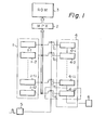
- Figure 1 is a block circuit diagram illustrating a circuit for reading out address data from a memory in a one-chip microcomputer. Referring to Fig. 1, only a part of the one-chip microcomputer is illustrated for highlighting the part pertaining to the present invention.
- a program counter 1 is connected through an address bus B and a multiplexer 2 to a ROM 3.
- Output terminals 1-1, 1-2, ..., and 1-12 are connected to drains (or sources) of metal oxide semiconductor (MOS) transistors T, , T 2 , ..., and T 12 , respectively.
- MOS metal oxide semiconductor
- the sources (or drains) of transistors T 1 , T 2 , ..., and T 12 are connected to a shift register 4.
- Shift register 4 consists of 12 stages 4-1 through 4-12. Stage 4-1 represents the most significant bit stage, while stage 4-12 represents the least significant bit stage. Thus, there is a one-to-one correspondence between the output terminals 1-1 through 1-12 and the 12 stages 4-1 through 4-12.
- transistors T 1 , T 2 , ..., and T 12 are commonly connected to an address output enable terminal 5 to which an enable signal is applied when the contents of program counter 1 are to be read out.
- transistors T 1 , T 2 , ..., and T 12 act as transfer gates for transferring data from program counter 1 to shift register 4.
- Each stage of shift register 4 is sequentially connected to the next lower bit stage.
- the least significant bit stage 4-12 is connected to an address output terminal 6.
- Address output enable terminal 5 and address output terminal 6 can be realized by utilizing common, existing input/output terminals, which a conventional microcomputer has, with address output enable terminal 5 and address output terminal 6. Therefore, no additional terminal is required for address output enable terminal 5 and address output teminal 6.
- program counter 1 When the contents of program counter 1 are to be read out, one pulse is applied to address output enable terminal 5 to turn on all of transistors T 1 , T 2 , ..., and T 12 . Then, the data stored in program counter 1 are transferred through transistors T 1 , T 2 , ..., and T 12 to the corresponding stages of shift register 4. After the pulse has been applied to address output enable terminal 5, all of transistors T 1 , T 2 ' ..., and T 12 are turned off again. Thus, program counter 1 is electrically separated from shift register 4. As a result, the contents of program counter 1, at the time when the pulse is applied to address output enable terminal 5, are stored in shift register 4, while, program counter 1 continues to operate to change its contents.
- a clock signal is applied to shift register 4 to read out the data stored therein.
- the contents of program counter 1 at the time when the pulse is applied to terminal 5 are outputted from address output terminal 6 in the sequence from the least significant bit to the most significant bit.
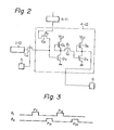
- FIG. 2 is a circuit diagram illustrating in detail the least significant bit stage 4-12 of shift register 4.
- Q 1 and Q 2 are data transferring transistors
- Q 3 and Q 5 are enhancement-type MOS transistors for storing data
- Q 4 and Q 6 are depletion-type MOS transistors functioning as load resistances.
- the drain (or source) of transistor Q 2 is connected to the output of preceding stage 4-11 of shift register 4.
- the source (or the drain) of transistor Q 2 and the source (or the drain) of transfer-gate transistor T 12 are commonly connected to the gate of transistor Q 3 .
- the drain (or the source) of transistor Q 4 is connected to power supply V CC .
- transistors Q 4 are commonly connected to the drain (or the source) of transistor Q 3 and to the gate of transistor Q 5 .
- the source (or the drain) of transistor Q 3 is grounded.
- transistors Q 3 and Q 4 constitute an inverter.
- Transistors Q 5 and Q 6 are wired similarly to the wiring of transistor Q 3 and Q 4 , to form another inverter.
- the output of the inverter that is, the commonly connecting point of the gate and the source (or the drain) of transistor Q 6 and drain (or source) of transistor Q 5 is connected to address output terminal 6.
- Clock signals ⁇ 1 and ⁇ 2 are applied to the gates of transistors Q 1 and Q 2 , respectively.
- Figure 3 is a waveform diagram illustrating clock signals 1 and ⁇ 2 applied to the gates of transistors Q 1 and Q 2 .
- clock signals ⁇ 1 and ⁇ 2 are generated alternately.
- the contents of program counter 1 are transferred through transfer-gate transistors T 1 through T 12 to shift register 4, as described with reference to Fig. 1.
- the least significant bit is transferred from output terminal 1-12 through transistor T 12 to transistor Q 3 and is stored therein.
- a pulse P 11 of clock signal ⁇ 1 is applied to the gate of transistor Q 1 so that the data stored in transistor Q 3 is transferred through transistor Q 1 to transistor Q 5 and stored therein.
- the data stored in transistor Q 5 is read out from the drain of transistor Q 5 to address output terminal 6.
- pulse P 21 of clock signal ⁇ 2 is applied to the gate of transistor Q 2 so that data stored in upper bit stage 4-11 is transferred through transistor Q 2 to transistor Q 3 and stored therein.
- data stored in upper bit stage 4-10 (not shown in Fig. 2, but shown in Fig. 1) is transferred to stage 4-11. Similar operations are effected regarding the other stages of shift register 4.
- the clock pulses of clock signals ⁇ 1 and ⁇ 2 sequentially, the data stored in shift register 4 are sequentially outputted from the least significant bit to the most significant bit.
- address output terminal 6 was connected to the least significant bit stage of shift register 4 so that the data were read out from the least significant bit.
- address output terminal 6 may be connected to the most significant bit stage for reading out data from the most significant bit.
- the program counter may alternatively consist of other than 12 bits in accordance with the number of addresses in the ROM to be accessed.
- address output enable terminal 5 and address output terminal 6 are physically separated from each other.
- these terminals 5 and 6 may be realized by one terminal including a switching circuit for selecting the signal line connected to the gates of transistors T1 through T 12 or the signal line connected to the drain of the transistor Q 5 .
- these terminals 5 and 6 may, according to the present invention, be newly added to the one-chip microcomputer.
- the address data stored in the shift register may alternatively be outputted in parallel.
- the contents of the program counter can be read out in a shorter time in comparison with conventional microcomputers. Also, since the address output enable terminal and the address output terminal are realized by existing input/output terminals, the contents of the program counter can be read out without adding any input/output terminal.
Abstract
A circuit for reading out addresses applied to a memory in a one-chip microcomputer which does not have any address terminals but has input/output terminals (5, 6). The circuit comprises a program counter (1) for specifying reading out addresses of the memory. Transfer gates (T) and a shift register (4) are provided. The transfer gates transfer the contents of the program counter to the shift register when an address output enable signal (at input terminal 5) is applied to the transfer gates. The contents stored in the shift register (4) are read out, generally in series by clock pulses, to an address output terminal (6) connected to the shift register, preferably at the most- or least-significant bit stage.
Description
- This invention relates to a circuit for reading out address data applied to a memory in a one-chip microcomputer, more particularly to a circuit for reading out reading-out address data of a memory in a one-chip microcomputer which does not have any address terminals but has input/output terminals to the outside.
- Generally, a one-chip microcomputer comprises a read-only memory (ROM) for storing a program and a program counter for executing the program by designating the addresses in the ROM. In mass-produced microcomputers, such as four-bit or eight-bit microcomputers (except evaluation chips for evaluating mass-produced chips), the ROM is a mask ROM type and the stored program is fixed in the mask ROM. Users generally do not have to rewrite or debug the stored program. Therefore, one-chip microcomputers do not have address output terminals for outputting the reading-out address of the ROM, i.e., the contents of the program counter (see, for example, TSM 1000 Series MOS/LSI ONE-CHIP MICROCOMPUTERS SOFTWARE User's GUIDE,TEXAS INSTRUMENTS Pages 1-1 1-8 and 105). However, during the manufacture of one-chip microcomputers or during the shipment of manufactured microcomputers, it is often required to investigate the contents of the program counter for debugging, functional tests, mounting tests, or analysis of bad chips.
- To enable investigation of the contents of the program counter from the outside of one-chip microcomputers terminals may be provided for outputting the addresses. However, the same number of terminals would be required for outputting addresses as the number of outputs of the program counter. When the memory capacity of a ROM is 4096 bytes, the program counter would have 12 outputs, as is known from the
equation 4096 = 2 12 . - Users of mass-produced microcomputers do not need the terminals for outputting addresses. Further, provision of the terminals for outputting addresses would increase the number of input/output terminals of one-chip microcomputers. Therefore, it is not preferable to provide output terminals used only for outputting addresses.
- An address output function could be provided to the original input/output terminals of one-chip microcomputers, but in this case, the wiring pattern would become so complex that the chip size would be increased.
- Conventionally, the contents of the program counter of a one-chip microcomputer (except evaluation chips) have been investigated by using signals obtained when the program counter overflows. For example, when the program counter outputs 12 bits for specifying an address among 0 address to 4095 address of the ROM, it overflows after outputting data 'FFF' (hexadecimal expression). Accordingly, when a jump instruction is provided, so that an' address of, for example, '555' (hexadecimal expression) is specified by the program counter, and when it is necessary to check whether the program counter correctly specifies the jumped address, it is necessary to wait until the program counter overflows, that is, it is necessary to wait until the steps of AAA (hexadecimal expression) because FFF - 555 = AAA. If the program counter correctly specified the jumped address, it provides an overflow signal after counting up the steps of AAA from the jump instruction.
- In this conventional method, therefore, while the contents of the program counter could be checked by counting the number of steps from the desired address to the overflow address, the necessity to wait until the program counter overflowed made the time required to make this check long.
- In view of the foregoing, it is a principal object of the present invention to decrease the read-out time for reading the contents of a program counter included in a one-chip microcomputer which does not have terminals used only for outputting the contents of the program counter, without adding any input/output terminals.
- This invention consists in a circuit for reading out address data applied to a memory in a one-chip microcomputer to the outside, comprising: a program counter having a plurality of outputs for specifying reading out addresses of said memory; and characterized by: a plurality of transfer gates, each having an input, an output, and a gate, each input being connected to one of the outputs of the program counter; a shift register comprising a plurality of stages, each stage having an input and an output, each input being connected to one of the outputs of the transfer gates; an address output enable terminal for receiving an address output enable signal, the output enable terminal being commonly connected to all of the said gates of the transfer gates, the outputs of the program counter being transferred through the transfer gates to the shift register when the address output enable signal is applied to the address output enable terminal; and an address output terminal for outputting the contents stored in the shift register, the address output terminal being connected to at least one of the outputs of the shift register.
- The invention will be better understood from the following more detailed description taken in conjunction with the accompanying drawings, in which:
- Fig. 1 is a block circuit diagram illustrating a circuit for reading out address data from a memory in a one-chip microcomputer, according to an embodiment of the present invention;
- Fig. 2 is a circuit diagram illustrating in detail a part of the circuit of Fig. 1; and
- Fig. 3 is a waveform diagram illustrating clock signals applied to the circuit of Fig. 2.
- An embodiment of the present invention will now be described with reference to the drawings.
- Figure 1 is a block circuit diagram illustrating a circuit for reading out address data from a memory in a one-chip microcomputer. Referring to Fig. 1, only a part of the one-chip microcomputer is illustrated for highlighting the part pertaining to the present invention. A
program counter 1 is connected through an address bus B and amultiplexer 2 to aROM 3.Program counter 1, in this embodiment, has 12 output terminals 1-1 through 1-12. Output terminal 1-1 outputs the most significant bit, while output terminal 1-12 represents the least significant bit. Accordingly, program counter 1 can specify one of 2 12 = 4096 addresses inROM 3. Output terminals 1-1, 1-2, ..., and 1-12 are connected to drains (or sources) of metal oxide semiconductor (MOS) transistors T, , T2 , ..., and T12 , respectively. The sources (or drains) of transistors T1, T2 , ..., and T12 on the other hand, are connected to ashift register 4.Shift register 4 consists of 12 stages 4-1 through 4-12. Stage 4-1 represents the most significant bit stage, while stage 4-12 represents the least significant bit stage. Thus, there is a one-to-one correspondence between the output terminals 1-1 through 1-12 and the 12 stages 4-1 through 4-12. The gates of transistors T1 , T2 , ..., and T12 are commonly connected to an address output enableterminal 5 to which an enable signal is applied when the contents ofprogram counter 1 are to be read out. Thus, transistors T1, T2 , ..., and T12 act as transfer gates for transferring data fromprogram counter 1 to shiftregister 4. Each stage ofshift register 4 is sequentially connected to the next lower bit stage. The least significant bit stage 4-12 is connected to an address output terminal 6. Address output enableterminal 5 and address output terminal 6 can be realized by utilizing common, existing input/output terminals, which a conventional microcomputer has, with address output enableterminal 5 and address output terminal 6. Therefore, no additional terminal is required for address output enableterminal 5 and address output teminal 6. During read-out of the contents ofprogram counter 1, the original function ofterminals 5 and 6, that is, the function as input/output terminals, is not necessary. Therefore, no problem is caused by utilizing these input/output terminals as address output enableterminal 5 and address output terminal 6. - When the contents of
program counter 1 are to be read out, one pulse is applied to address output enableterminal 5 to turn on all of transistors T1 , T2 , ..., and T12. Then, the data stored inprogram counter 1 are transferred through transistors T1 , T2 , ..., and T12 to the corresponding stages ofshift register 4. After the pulse has been applied to address output enableterminal 5, all of transistors T1 , T2 ' ..., and T12 are turned off again. Thus,program counter 1 is electrically separated fromshift register 4. As a result, the contents ofprogram counter 1, at the time when the pulse is applied to address output enableterminal 5, are stored inshift register 4, while,program counter 1 continues to operate to change its contents. As described in detail in the following, a clock signal is applied to shiftregister 4 to read out the data stored therein. Thus, the contents ofprogram counter 1 at the time when the pulse is applied toterminal 5 are outputted from address output terminal 6 in the sequence from the least significant bit to the most significant bit. - Figure 2 is a circuit diagram illustrating in detail the least significant bit stage 4-12 of
shift register 4. Referring to Fig. 2, Q1 and Q2 are data transferring transistors; Q3 and Q5 are enhancement-type MOS transistors for storing data; and Q4 and Q6 are depletion-type MOS transistors functioning as load resistances. The drain (or source) of transistor Q2 is connected to the output of preceding stage 4-11 ofshift register 4. The source (or the drain) of transistor Q2 and the source (or the drain) of transfer-gate transistor T12 are commonly connected to the gate of transistor Q3. The drain (or the source) of transistor Q4 is connected to power supply VCC. The gate and the source (or the drain) of transistor Q4 are commonly connected to the drain (or the source) of transistor Q3 and to the gate of transistor Q5. The source (or the drain) of transistor Q3 is grounded. Thus, transistors Q3 and Q4 constitute an inverter. Transistors Q5 and Q6 are wired similarly to the wiring of transistor Q3 and Q4 , to form another inverter. The output of the inverter, that is, the commonly connecting point of the gate and the source (or the drain) of transistor Q6 and drain (or source) of transistor Q5 is connected to address output terminal 6. Clock signals ϕ1 and ϕ2 are applied to the gates of transistors Q1 and Q2, respectively. - Figure 3 is a waveform diagram illustrating
clock signals 1 and ϕ2 applied to the gates of transistors Q1 and Q2. Referring to Figs. 2 and 3, the read-out operation ofprogram counter 1 will be described in detail. As illustrated in Fig. 3, clock signals φ1 and φ2 are generated alternately. When a pulse signal is applied to address output enableterminal 5, the contents ofprogram counter 1 are transferred through transfer-gate transistors T1 through T12 to shiftregister 4, as described with reference to Fig. 1. In Fig. 2, the least significant bit is transferred from output terminal 1-12 through transistor T12 to transistor Q3 and is stored therein. Then, a pulse P11 of clock signal φ1 is applied to the gate of transistor Q1 so that the data stored intransistor Q 3 is transferred through transistor Q1 to transistor Q5 and stored therein. The data stored in transistor Q5 is read out from the drain of transistor Q5 to address output terminal 6. After this, pulse P21 of clock signal φ2 is applied to the gate of transistor Q2 so that data stored in upper bit stage 4-11 is transferred through transistor Q2 to transistor Q3 and stored therein. Simultaneously, data stored in upper bit stage 4-10 (not shown in Fig. 2, but shown in Fig. 1) is transferred to stage 4-11. Similar operations are effected regarding the other stages ofshift register 4. By applying the clock pulses of clock signals φ1 and φ2 sequentially, the data stored inshift register 4 are sequentially outputted from the least significant bit to the most significant bit. - In the embodiment described above, address output terminal 6 was connected to the least significant bit stage of
shift register 4 so that the data were read out from the least significant bit. Alternatively, address output terminal 6 may be connected to the most significant bit stage for reading out data from the most significant bit. - The program counter may alternatively consist of other than 12 bits in accordance with the number of addresses in the ROM to be accessed.
- In the above described embodiment, address output enable
terminal 5 and address output terminal 6 are physically separated from each other. Alternatively, theseterminals 5 and 6 may be realized by one terminal including a switching circuit for selecting the signal line connected to the gates of transistors T1 through T12 or the signal line connected to the drain of the transistor Q5. - Still further, instead of using the existing input/ output terminals as address output enable
terminal 5 and address output terminal 6, theseterminals 5 and 6 may, according to the present invention, be newly added to the one-chip microcomputer. - Still further, instead of sequentially outputting the address data from the shift register in response to the clock signals, the address data stored in the shift register may alternatively be outputted in parallel.
- From the foregoing description, it will be apparent that, according to the present invention, in a one-chip microcomputer not having a terminal used only for outputting the contents of a program counter, the contents of the program counter can be read out in a shorter time in comparison with conventional microcomputers. Also, since the address output enable terminal and the address output terminal are realized by existing input/output terminals, the contents of the program counter can be read out without adding any input/output terminal.
Claims (8)
1. A circuit for reading out address data applied to a memory (3) in a one-chip microcomputer to the outside, comprising:
a program counter (1) having a plurality of outputs (1-1 to 1-12) for specifying reading out addresses of said memory; and characterized by:
a plurality of transfer gates (Tl to T12), each having an input, an output, and a gate, each input being connected to one of the outputs of the program counter;
a shift register (4) comprising a plurality of stages (4-1 to 4-12), each/having an input and an output, each input being connected to one of the outputs of the transfer gates;
an address output enable terminal (5) for receiving an address output enable signal, the output enable terminal being commonly connected to all of the gates of the transfer gates, the outputs of the program counter being transferred through the transfer gates to the shift register when the address output enable signal is applied to the address output enable terminal; and
an address output terminal (6) for outputting the contents stored in the shift register(4), the address output terminal being connected to at least one of the outputs of the shift register.
2. A circuit as set forth in claim 1, wherein each of the transfer gates comprises a metal oxide semiconductor transistor.
3. A circuit as set forth in claim 1 or 2, wherein the memory comprises a read-only memory (3).
4. A circuit as set forth in claim 1, 2, or 3, wherein the stages of the shift register (4) comprise the stages from the least significant bit stage (4-12) to the most significant bit stage (4-1).
5. A circuit as set forth in claim 4, wherein the address output terminal (6) is connected to the output of the least significant bit stage (4-12).
6. A circuit as set forth in claim 4, wherein the address output terminal is connected to the output of the most significant bit stage (4-1).
7. A circuit as set forth in claim 5 or 6, wherein the contents stored in the shift register (4) are outputted in series from the address output terminal (6) in response to clock signals (φ1,φ2) applied to the shift register.
8. A circuit as set forth in any one of claims 1 through 4, wherein the address output terminal is adapted to output in parallel the contents of the shift register (4).
Applications Claiming Priority (2)
| Application Number | Priority Date | Filing Date | Title |
|---|---|---|---|
| JP97396/81 | 1981-06-25 | ||
| JP9739681A JPS57212563A (en) | 1981-06-25 | 1981-06-25 | Address reading circuit for one-chip microcomputer |
Publications (1)
| Publication Number | Publication Date |
|---|---|
| EP0069509A1 true EP0069509A1 (en) | 1983-01-12 |
Family
ID=14191351
Family Applications (1)
| Application Number | Title | Priority Date | Filing Date |
|---|---|---|---|
| EP82303282A Ceased EP0069509A1 (en) | 1981-06-25 | 1982-06-23 | A circuit for reading out address data applied to a memory in a one-chip microcomputer |
Country Status (3)
| Country | Link |
|---|---|
| US (1) | US4513400A (en) |
| EP (1) | EP0069509A1 (en) |
| JP (1) | JPS57212563A (en) |
Cited By (1)
| Publication number | Priority date | Publication date | Assignee | Title |
|---|---|---|---|---|
| EP0489944A1 (en) * | 1990-12-08 | 1992-06-17 | Deutsche ITT Industries GmbH | Master-slave data communication method with flexible one-wire bus |
Families Citing this family (4)
| Publication number | Priority date | Publication date | Assignee | Title |
|---|---|---|---|---|
| JPS61222148A (en) * | 1985-03-08 | 1986-10-02 | Fujitsu Ltd | Manufacture of one-chip microcomputer |
| JP3469941B2 (en) * | 1994-07-15 | 2003-11-25 | 三菱電機株式会社 | Program execution control device and method |
| JP3540844B2 (en) * | 1994-11-02 | 2004-07-07 | 日本テキサス・インスツルメンツ株式会社 | Semiconductor integrated circuit |
| US5611068A (en) * | 1994-12-27 | 1997-03-11 | Motorola, Inc. | Apparatus and method for controlling pipelined data transfer scheme between stages employing shift register and associated addressing mechanism |
Citations (3)
| Publication number | Priority date | Publication date | Assignee | Title |
|---|---|---|---|---|
| US3939452A (en) * | 1972-07-14 | 1976-02-17 | Ing. C. Olivetti & C., S.P.A. | Desk-top electronic computer with MOS circuit logic |
| GB1542135A (en) * | 1975-04-21 | 1979-03-14 | Siemens Ag | Integrated circuit modules for use in data processing systems |
| GB2023341A (en) * | 1978-06-06 | 1979-12-28 | Siemens Ag | Improvements in or relating to monolithic integrated semiconductor digital circuit modules |
Family Cites Families (4)
| Publication number | Priority date | Publication date | Assignee | Title |
|---|---|---|---|---|
| GB202341A (en) * | 1922-03-10 | 1923-08-10 | Michael Nathanial Jacobson | Improvements in stair carpet holders |
| US3708690A (en) * | 1971-02-22 | 1973-01-02 | Mos Technology Inc | Shift register |
| JPS5939775B2 (en) * | 1978-03-06 | 1984-09-26 | 株式会社東芝 | Memory addressing scheme |
| JPS5515271A (en) * | 1978-07-19 | 1980-02-02 | Nissin Electric Co Ltd | Oillfilled capacitor |
-
1981
- 1981-06-25 JP JP9739681A patent/JPS57212563A/en active Granted
-
1982
- 1982-06-22 US US06/390,875 patent/US4513400A/en not_active Expired - Lifetime
- 1982-06-23 EP EP82303282A patent/EP0069509A1/en not_active Ceased
Patent Citations (3)
| Publication number | Priority date | Publication date | Assignee | Title |
|---|---|---|---|---|
| US3939452A (en) * | 1972-07-14 | 1976-02-17 | Ing. C. Olivetti & C., S.P.A. | Desk-top electronic computer with MOS circuit logic |
| GB1542135A (en) * | 1975-04-21 | 1979-03-14 | Siemens Ag | Integrated circuit modules for use in data processing systems |
| GB2023341A (en) * | 1978-06-06 | 1979-12-28 | Siemens Ag | Improvements in or relating to monolithic integrated semiconductor digital circuit modules |
Non-Patent Citations (1)
| Title |
|---|
| IBM TECHNICAL DISCLOSURE BULLETIN, vol. 17, no. 9, February 1975, pages 2654,2655, New York (USA); * |
Cited By (3)
| Publication number | Priority date | Publication date | Assignee | Title |
|---|---|---|---|---|
| EP0489944A1 (en) * | 1990-12-08 | 1992-06-17 | Deutsche ITT Industries GmbH | Master-slave data communication method with flexible one-wire bus |
| US5237322A (en) * | 1990-12-08 | 1993-08-17 | Deutsche Itt Industries Gmbh | Master-slave data transmission system employing a flexible single-wire bus |
| US5495240A (en) * | 1990-12-08 | 1996-02-27 | Deutsche Itt Industries Gmbh | Master-slave data transmission system employing a flexible single-wire bus |
Also Published As
| Publication number | Publication date |
|---|---|
| JPS6244304B2 (en) | 1987-09-19 |
| US4513400A (en) | 1985-04-23 |
| JPS57212563A (en) | 1982-12-27 |
Similar Documents
| Publication | Publication Date | Title |
|---|---|---|
| US5088027A (en) | Single-chip microcomputer | |
| US5305284A (en) | Semiconductor memory device | |
| KR940002755B1 (en) | One-chip microcomputer | |
| EP0051920A2 (en) | Memory arrangement with means for interfacing a central processing unit | |
| EP0243113B1 (en) | Data processor | |
| US5019970A (en) | IC card | |
| KR890005622A (en) | Single chip microcomputer | |
| US5710734A (en) | Semiconductor memory device and data writing method thereof | |
| US4513400A (en) | Circuit for reading out address data applied to a memory in a one-chip microcomputer | |
| KR880001972Y1 (en) | Sewing machine with memory input recontiguration based on type of memory being used | |
| US5247521A (en) | Data processor | |
| KR100205847B1 (en) | Information processing apparatus with a mode setting circuit | |
| US5164918A (en) | Integrated circuit | |
| US5948114A (en) | Integrated circuit binary data output interface for multiplexed output of internal binary information elements from input/output pads | |
| US5126972A (en) | Arrangement and method of ascertaining memory addresses which have been accessed during program execution | |
| US6385073B1 (en) | Integrated circuit device with expandable nonvolatile memory | |
| JP2583055B2 (en) | IC test system | |
| EP0157342A2 (en) | Memory address expansion system | |
| JPS646489B2 (en) | ||
| JP2692408B2 (en) | Built-in diagnostic circuit in large scale integrated circuit | |
| SU1236552A1 (en) | Read-only memory | |
| SU1026163A1 (en) | Information writing/readout control device | |
| KR940001104B1 (en) | Method and circuit for power reset and manual reset | |
| JPH0679278B2 (en) | Microcomputer development equipment | |
| KR920005293B1 (en) | Memory address allocational method and apparatus for data processing device |
Legal Events
| Date | Code | Title | Description |
|---|---|---|---|
| PUAI | Public reference made under article 153(3) epc to a published international application that has entered the european phase |
Free format text: ORIGINAL CODE: 0009012 |
|
| AK | Designated contracting states |
Designated state(s): DE FR GB |
|
| 17P | Request for examination filed |
Effective date: 19830629 |
|
| STAA | Information on the status of an ep patent application or granted ep patent |
Free format text: STATUS: THE APPLICATION HAS BEEN REFUSED |
|
| 18R | Application refused |
Effective date: 19880503 |
|
| APAF | Appeal reference modified |
Free format text: ORIGINAL CODE: EPIDOSCREFNE |
|
| RIN1 | Information on inventor provided before grant (corrected) |
Inventor name: MASAKI, SATORU |