EP0063659B1 - Control marking detector - Google Patents
Control marking detector Download PDFInfo
- Publication number
- EP0063659B1 EP0063659B1 EP81303069A EP81303069A EP0063659B1 EP 0063659 B1 EP0063659 B1 EP 0063659B1 EP 81303069 A EP81303069 A EP 81303069A EP 81303069 A EP81303069 A EP 81303069A EP 0063659 B1 EP0063659 B1 EP 0063659B1
- Authority
- EP
- European Patent Office
- Prior art keywords
- radiation
- detector
- input
- output
- web
- Prior art date
- Legal status (The legal status is an assumption and is not a legal conclusion. Google has not performed a legal analysis and makes no representation as to the accuracy of the status listed.)
- Expired
Links
- 230000005855 radiation Effects 0.000 claims abstract description 91
- 230000008859 change Effects 0.000 claims abstract description 11
- 230000004044 response Effects 0.000 claims description 17
- 238000001514 detection method Methods 0.000 claims description 9
- 230000002238 attenuated effect Effects 0.000 claims description 2
- 230000008878 coupling Effects 0.000 claims 1
- 238000010168 coupling process Methods 0.000 claims 1
- 238000005859 coupling reaction Methods 0.000 claims 1
- 230000005670 electromagnetic radiation Effects 0.000 abstract description 11
- 239000003990 capacitor Substances 0.000 description 12
- 238000004519 manufacturing process Methods 0.000 description 5
- 239000000463 material Substances 0.000 description 5
- 230000035945 sensitivity Effects 0.000 description 4
- 239000000990 laser dye Substances 0.000 description 3
- 239000000126 substance Substances 0.000 description 3
- 230000007423 decrease Effects 0.000 description 2
- 239000002966 varnish Substances 0.000 description 2
- 230000009471 action Effects 0.000 description 1
- 230000004913 activation Effects 0.000 description 1
- 230000004075 alteration Effects 0.000 description 1
- 150000001875 compounds Chemical class 0.000 description 1
- 239000012141 concentrate Substances 0.000 description 1
- 230000001186 cumulative effect Effects 0.000 description 1
- 230000001419 dependent effect Effects 0.000 description 1
- 238000004146 energy storage Methods 0.000 description 1
- 238000001914 filtration Methods 0.000 description 1
- 238000002329 infrared spectrum Methods 0.000 description 1
- 238000000034 method Methods 0.000 description 1
- 230000004048 modification Effects 0.000 description 1
- 238000012986 modification Methods 0.000 description 1
- 238000004806 packaging method and process Methods 0.000 description 1
- 230000008569 process Effects 0.000 description 1
- 230000009467 reduction Effects 0.000 description 1
- 238000002310 reflectometry Methods 0.000 description 1
- 230000003252 repetitive effect Effects 0.000 description 1
- 238000007493 shaping process Methods 0.000 description 1
- 238000001228 spectrum Methods 0.000 description 1
- 239000002699 waste material Substances 0.000 description 1
Images
Classifications
-
- B—PERFORMING OPERATIONS; TRANSPORTING
- B65—CONVEYING; PACKING; STORING; HANDLING THIN OR FILAMENTARY MATERIAL
- B65H—HANDLING THIN OR FILAMENTARY MATERIAL, e.g. SHEETS, WEBS, CABLES
- B65H23/00—Registering, tensioning, smoothing or guiding webs
- B65H23/04—Registering, tensioning, smoothing or guiding webs longitudinally
- B65H23/046—Sensing longitudinal register of web
Definitions
- This invention relates to a radiation detector and more particularly to a detector adapted to sense the presence of indicia on an article such as a web moving in relation to the detector to control one or more control functions to be performed on or with the article.
- Radiation detectors useful in scanning moving objects which contain position coordinating indicia are known in the art.
- detectors employ visible radiation sensitive detectors which scan an object for the presence of a visible mark fixed to or forming a portion of the object. Once the indicia or marking is detected, it is known that the object being scanned is positioned at a particular point in relation to the detector. This information makes it possible to coordinate movement control and/or use of the object in response to control signals generated by the detector.
- One of the marking schemes for use with the herein disclosed detector utilizes a laser dye ink for affixing control indicia onto a web.
- the laser dye indicia emit nonvisible wavelength-shifted radiation in the infrared spectrum when exposed to high-intensity electromagnetic radiation of an appropriate wavelength.
- Another scheme utilizes a chemical marketed by Sandoz Chemicals under the tradename TH-40.
- the indicia ink made with Sandoz TH-40 forms an ordinarily invisible mark which emits wavelength-shifted electromagnetic radiation when exposed to incident radiation of an appropriate spectrum.
- a system has been proposed which utilizes indicia and a detector to control operations to and use of a moving web. When the indicia are irradiated with electromagnetic energy of a predetermined wavelength, the indicia emit electromagnetic radiation shifted in wavelength, which can be detected and used to generate control signals.
- Marking schemes used with webs have presented problems when the marks or indicia were affixed to multicolored or varying backgrounds.
- plastic webs used in the packaging art often include colorful designs and/ or logo areas which are different for various webs.
- Detection of the position-indicating marks on varying backgrounds has presented problems due to the variability in radiation reflected from the web.
- a detector which responds only to radiation intensities can be "fooled" when marks are affixed to different backgrounds that reflect light to different degrees.
- An absolute-intensity- level radiation detector might generate the same output signals from a good reflector, such as a light-colored background having no marking, and from a control mark that fluoresces on a dark background. The detector may therefore erroneously initiate a control where none is appropriate.
- This problem with the prior art radiation detectors stems from an inability to distinguish radiation from a control mark and reflected radiation from the web and/or ambient radiation in the vicinity of the detector.
- the detector may respond to a broad range of incident electromagnetic radiation of varying wavelengths even though the control marks emit only a narrow range of radiation.
- U.S.-A-3 600 589 discloses a detector for sensing the presence of a mark on an article comprising a radiation responsive means for sensing radiation intensity and circuitry coupled to the radiation responsive means to generate an output signal in response to abrupt changes of predetermined magnitude in the sensed radiation intensity by isolating the change which occurs between the presence or absence of a mark.
- the precharacterising portion of claim 1 is based on the disclosure of this citation.
- the present invention overcomes possible inaccuracies in prior art detecting systems by providing a detector that reliably senses the presence of a mark on a moving article even though the mark appears on varying backgrounds. In particular, it reduces the incidence of spurious control signals and misregistration of the moving article caused by an inability of prior art detectors to discriminate between a mark and a reflective background.
- a detector for sensing the presence of a mark on an article advanced along a defined path of travel comprising radiation responsive means (36) for sensing radiation intensity and circuitry (30) coupled to the radiation responsive means (36) to generate an output signal in response to abrupt changes of predetermined magnitude in said sensed radiation intensity characterised by:
- the marking is chosen to re-emit radiation of a particular narrow wavelength
- the filter enhances the sensitivity of the detector by causing it to respond primarily to the narrow band of radiation rather than to all ambient radiation in the region of the article.
- the invention includes a radiation responsive element mounted in close relation to a path of travel of a web.
- a source of electromagnetic radiation of a predetermined wavelength is mounted in close proximity to the path to cause marks on the web to emit wavelength-shifted radiation as the marks pass the radiation-responsive element.
- a filter which transmits the wavelength-shifted radiation but attenuates all other wavelengths of light, is interposed between the web and the radiation responsive element. Circuitry coupled to the element generates a control output signal only in response to abrupt changes in intensity of radiation of the wave-shifted length. The occurrence of an output signal is an indication that a control mark leading edge has been detected and can be used to coordinate web movement with fabrication or other process functions.
- the circuitry includes a differential amplifier having a first input coupled to the radiation responsive element and a second input feedback coupled to an amplifier output through an energy storage device.
- the feedback coupled input causes the second input to track or follow the first input for slowly varying changes in or for a constant level of the first input. Due to this feedback circuitry the output from the differential amplifier only changes in response to rapid changes in the input from the radiation responsive element.
- the differential amplifier output is coupled to circuitry that allows the user to tune the detector so that a change in radiation intensity, to be detectable, must not only be abrupt but also of a certain amplitude. This feature presents a safeguard against false detector activation by the web background, since changes in radiation intensity caused by variations in the web background are typically not great enough to produce a differential amplifier output once the circuitry has been tuned.
- the detector discounts a constant or slowly changing base level intensity of the ambient or incident radiation reflected by the web.
- mere pattern variations on the web, as distinguished from wave-shifting marks will not create a sufficient increase in intensity of reflected radiation to trigger a response by the detector, notwithstanding a situation where the total intensity level is created largely by a relatively high base level intensity- possibly as high as a level sufficient to trigger a response from a wave-shifting mark on a much less-reflective web.
- the amplifier feedback input also avoids problems in detector operation caused by temperature variations. Detectors that use absolute value sensors may change in their operating characteristics so the change in incident radiation needed to trigger the detector becomes very small. When this occurs problems caused by variation in web background are exacerbated.
- the feedback circuitry of the present invention avoids detector sensitivity changes with temperature because the change in feedback signal to the amplifier with circuitry temperature variations is gradual, whereas detector response requires rapid changes in the feedback signal.
- certain waveform-shaping amplifiers are included in the circuitry, which cause a well defined square wave output signal to be generated in response to the presence of the marking on the web.
- the time duration of this square wave output may be controlled to provide a signal particularly adapted for a particular web control system.
- one object of the present invention is the provision of a detector that is sensitive to changes in radiation intensity caused by markings affixed to a moving web.
- the detector avoids misregistration of the web by responding only to changes in light intensities rather than absolute intensity levels.
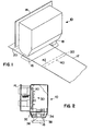
- FIGURE 1 a preferred detector unit 10 for detecting the presence of markings along a web is shown in FIGURE 1.
- This unit is mounted in proximity to a moving web 12 by a detector mounting plate 14.
- the web 12 is caused to move beneath the detector by an appropriate drive (not shown).
- a web guide 16 is positioned beneath the detector 10 and is attached to it by a suitable support 18. This guide 16 allows the web to pass beneath the detector at a distance close enough to allow the detector to sense the presence of marks 20 on the web.
- Control circuitry 30 mounted inside the unit 10 (see FIGURE 2) generates signals which control fabrication or manufacturing processes to be performed to the moving web as the marks 20 move past the detector.
- One material suitable for use as the marks 20 comprises KODAK I.R. 125, a laser dye, mixed with a clear varnish vehicle.
- a mark printed with this material emits nonvisible wavelength shifted electromagnetic radiation of about 9400 angstroms when exposed to incident radiation of about 7950 angstroms.
- Another comprises an ionic fluorescing compound sold by The Sandoz Chemical Company under the tradename TH-40.
- TH-40 When mixed with a suitable varnish the TH-40 is transparent and when illuminated with ultraviolet radiation of about 3600 angstroms emits visible light radiation of about 4500 angstroms.
- the detector unit 10 Mounted inside the detector unit 10 are two sources 32, 34 of electromagnetic radiation, e.g., infra red or ultra-violet radiation. Positioned between these sources is a photo diode 36 which senses the presence of the markings 20 on the web 12 as the web passes over the web guide 16.
- the sources 32, 34 concentrate radiation, such as infra red radiation of about 7950 angstroms or ultraviolet light of about 3660 angstroms, to an area of the web directly beneath the photo diode 36. When the incident radiation strikes a mark 20 it causes a wavelength shifted output to be emitted from that mark.
- a filter 38 for filtering out electromagnetic radiation of wavelengths other than the wavelength shifted radiation emitted by the marks.
- the filter 38 enhances sensitivity by preventing ambient, web-reflected, or incident radiation of a wavelength other than the wavelength-shifted radiation emitted by the marks from reaching the detector.
- Mark detection is enhanced by constructing the web guide support 18 to be adjustable to allow the distance between the web and the photo diode 36 to be optimized.
- Exemplary circuitry 30 for generating control voltages in response to the presence of the web markings is shown mounted inside the detector unit 10 on a printed circuit board 110. That circuitry 30 is electrically connected to the photo diode 36 in the detector unit 10. Three amplifiers 112, 114, 116 respond to changes in photo diode resistance with changes in electromagnetic radiation intensity from the marking 20 to generate an output 118 to a flip flop 120. When this output goes high it is an indication that a leading edge 40 (FIGURE 1) of a mark 20 has passed beneath the detector.
- FOGURE 1 leading edge 40
- the anode of that diode 36 is connected to a 12 volt source and the cathode is coupled through a 1 megohm resistor to a voltage divider 122.
- This amplifier 112 is an operational amplifier, one such suitable amplifier being an LM324 op amp.
- the other operational amplifiers shown in FIGURE 3 may also comprise LM324 op amps.
- An output 124 from the first operational amplifier 112 is coupled to a second operational amplifier 114 and is further coupled to the inverting input of the first op amp 112 through a feedback network 126, which includes the third amplifier 116.
- the second op amp 114 includes a reference input and a noninverting input connected to the output 124. When the noninverting input signal is greater than the reference signal at the inverting input, the output 118 from the second operational amplifier 114 goes high.
- This output 118 is coupled to the flip flop 120 which serves to shape the irregular-shaped output 118 from the second amplifier 114 into a well defined output 125 of constant height and pulse width.
- the pulse width of this output 125 is determined by an RC network 128 coupled to pin 4 of the flip flop 120 through an output amplifier 129.
- the output 118 goes high and a well defined voltage output from the flip flop is generated which can be used for control purposes.
- a well defined voltage output from the flip flop is generated which can be used for control purposes.
- the RC network 128 charges in response to a high output at flip flop pin #1, a one microfarad capacitor charges until a rest signal appears at pin 4.
- the circuitry is particularly suited to sense changes in the radiation level caused by the wavelength-shifting marks and to distinguish those changes from background light intensity due to the type and color of the background web material supporting the markings.
- a light-colored or transparent web produces a higher ambient or background level of light than a dark-colored web so that markings on a dark background may provide less intense radiation than a web area with no markings but with a light background. For this reason the circuitry must be sensitive to changes in intensity and not merely to absolute intensity levels.
- the feedback network 126 provides this capability.
- the feedback network 126 provides negative feedback to the amplifier 112 to minimize the response of that amplifier to gradual changes in sensed radiation intensity, yet enables the amplifier 112 to remain sensitive to abrupt changes in sensed radiation levels of predetermined magnitudes.
- the preferred feedback network 126 comprises two parallel-connected diode, resistor circuits 130, 132, a 10 microfarad capacitor 136 and the third amplifier 116.
- the capacitor 136 is charged via the circuit 130 which includes a forward biased diode 133 and a 1 megohm resistor 134. As the capacitor 136 charges the voltage across it increases. This voltage level is coupled to the noninverting input of the third amplifier 116 whose output is transmitted to the inverting input of the first amplifier 112.
- the capacitor 136 charges slowly so that the feedback input to the first amplifier's inverting input also changes slowly, trailing the non- inverting input to the first amplifier. Since the output from the first amplifier is the difference in value between its two inputs, the signal 124 transmitted to the second amplifier 114 tends to be constant or relatively so in response to relatively gradual increases in sensed radiation levels.
- the output from the amplifier 112 When sensed radiation levels are gradually reduced the output from the amplifier 112 likewise tends to be reduced.
- This reduction in the voltage level of the output 124 permits the capacitor 136 to discharge through the circuit 132 which includes a diode 137, poled oppositely to the diode 133, and a 330 ohm resistor connected between the capacitor 136 and the output line 124.
- the capacitor 136 discharges gradually at the rate dependent upon the voltage level of the output 124.
- the signal level input to the amplifier 116 is reduced and the reduced output from the amplifier 116 tends to increase the output signal level from the amplifier 112.
- the feedback network capacitor 136 cannot charge rapidly enough through the resistor 134 to significantly change the input to the feedback amplifier 116.
- the inverting input of the first amplifier then does not change appreciably until the flip flop has already generated its control output. From the above it is apparent that the circuitry 110 is sensitive to rapid increases in radiation intensity; but not to gradual changes in sensed radiation intensity.
- Temperature variations in the vicinity of the detector unit 10 affect output of the amplifier 112 in a similar manner to variations in ambient light or web reflectivity. As the temperature increases, the conductivity of the diode 36 increases, but typically at a slow rate.
- the feedback network 126 responds to this change in diode current and causes the signal at the first amplifier's inverting input to track the slowly varying (with temperature) signal at the non-inverting (+) input. This slow increase in current does not reduce the magnitude of the rapid change in current level required to produce a signal at the noninverting input to the second amplifier 114, which triggers the flip flop 120. Therefore, notwithstanding a temperature increase, the detector does not become responsive to changes in light intensity of somewhat less magnitude than produced from wave-shifting marks.
- the output signal 124 from the first amplifier 112 passes through a variable rheostat 138 before reaching the noninverting input to the second amplifier 114.
- a variable rheostat 138 By adjusting the setting of this rheostat 138 during setup the user can optimize detector operation and sensitivity.
- Adjustment of the rheostat 138 during detector setup insures the detector output is in response to abrupt changes in wave-shifted radiation from the markings 20 and not abrupt smaller changes in reflected light from the web 12.
- the rheostat setting is adjusted until the second amplifier 114 responds only to abrupt rather large changes in current through the diode 36 rather than abrupt small changes that might be caused by changes in the background web pattern.
- a feedback resistor 140 gives the second amplifier hysteresis action and prevents that amplifier from oscillating on and off in the event the first amplifier output 124 is very close to the six volts provided by the voltage divider 122 to the inverting input to this second amplifier 114.
Landscapes
- Length Measuring Devices By Optical Means (AREA)
- Geophysics And Detection Of Objects (AREA)
- Controlling Rewinding, Feeding, Winding, Or Abnormalities Of Webs (AREA)
- Drying Of Semiconductors (AREA)
- Acyclic And Carbocyclic Compounds In Medicinal Compositions (AREA)
- Mechanical Treatment Of Semiconductor (AREA)
- Optical Transform (AREA)
Priority Applications (1)
| Application Number | Priority Date | Filing Date | Title |
|---|---|---|---|
| AT81303069T ATE22428T1 (de) | 1981-04-27 | 1981-07-06 | Markenabtastgeraet. |
Applications Claiming Priority (2)
| Application Number | Priority Date | Filing Date | Title |
|---|---|---|---|
| US06/253,193 US4392056A (en) | 1981-04-27 | 1981-04-27 | Control marking detector |
| US253193 | 1981-04-27 |
Publications (2)
| Publication Number | Publication Date |
|---|---|
| EP0063659A1 EP0063659A1 (en) | 1982-11-03 |
| EP0063659B1 true EP0063659B1 (en) | 1986-09-24 |
Family
ID=22959270
Family Applications (1)
| Application Number | Title | Priority Date | Filing Date |
|---|---|---|---|
| EP81303069A Expired EP0063659B1 (en) | 1981-04-27 | 1981-07-06 | Control marking detector |
Country Status (6)
| Country | Link |
|---|---|
| US (1) | US4392056A (fi) |
| EP (1) | EP0063659B1 (fi) |
| JP (1) | JPS57180554A (fi) |
| AT (1) | ATE22428T1 (fi) |
| CA (1) | CA1171154A (fi) |
| DE (1) | DE3175376D1 (fi) |
Cited By (1)
| Publication number | Priority date | Publication date | Assignee | Title |
|---|---|---|---|---|
| DE4432371A1 (de) * | 1994-09-12 | 1996-03-14 | Heidelberger Druckmasch Ag | Verfahren zur Erfassung fehlerhafter Einzelnutzen beim Nutzendruck |
Families Citing this family (19)
| Publication number | Priority date | Publication date | Assignee | Title |
|---|---|---|---|---|
| US4590859A (en) * | 1982-06-30 | 1986-05-27 | Monarch Marking Systems, Inc. | Method of printing by sensing variable indicia tag format length |
| US4533926A (en) * | 1982-12-23 | 1985-08-06 | American Home Products Corporation (Del.) | Strip chart recorder and medium status |
| US5265402A (en) * | 1989-08-18 | 1993-11-30 | Automated Packaging Systems, Inc. | Packaging machine |
| US5077958A (en) * | 1989-08-18 | 1992-01-07 | Automated Packaging Systems, Inc. | Packaging machine and method |
| US5070674A (en) * | 1989-08-18 | 1991-12-10 | Automated Packaging Systems, Inc. | Packaging machine and method |
| US5015849A (en) * | 1989-12-14 | 1991-05-14 | Milliken Research Corporation | Index marking system |
| DE69103714T2 (de) * | 1990-10-01 | 1995-04-20 | Eastman Kodak Co | Spektralphotometer mit Mitteln zur gleichzeitigen Modulierung, Umschaltung und Wellenlängenauswahl einer Lichtquelle. |
| JP2733135B2 (ja) * | 1990-11-20 | 1998-03-30 | 富士通株式会社 | 光学読取装置のレーザー発生制御方式 |
| US5458062A (en) * | 1994-02-28 | 1995-10-17 | Goldberg; Ira B. | Continuous web printing press with page cutting control apparatus and method |
| DE4427978A1 (de) * | 1994-08-08 | 1996-02-15 | Heidelberger Druckmasch Ag | Verfahren zum Überwachen einer Numeriereinrichtung in einer Druckmaschine |
| US5682331A (en) * | 1996-01-05 | 1997-10-28 | Xerox Corporation | Motion tracking using applied thermal gradients |
| US6027820A (en) * | 1996-01-11 | 2000-02-22 | Jps Packaging Co. | Continuous web registration |
| US6746053B1 (en) * | 1998-10-29 | 2004-06-08 | International Business Machines Corporation | Method and system for preventing parallel marketing of wholesale and retail items |
| US6550226B1 (en) | 1999-10-27 | 2003-04-22 | Gates Automation, Inc. | Bag filling and sealing machine and method for handling bags |
| US6742321B2 (en) | 2002-09-30 | 2004-06-01 | Gates Automation, Inc. | Flange alignment and grasping assembly for bag handling apparatus |
| US7832553B2 (en) * | 2006-03-17 | 2010-11-16 | Illinois Tool Works Inc. | Heat-shrinkable holder for articles, heat-shrinkable package of articles, heat-shrinkable sleeve for articles, and method and device for packaging and sleeving articles |
| US7861490B2 (en) * | 2006-03-17 | 2011-01-04 | Illinois Tool Works Inc. | Method of packaging articles |
| US7850003B2 (en) | 2006-03-17 | 2010-12-14 | Illinois Tool Works Inc. | Heat-shrinkable holder for articles, heat-shrinkable package of articles, and method of packaging articles |
| US9623622B2 (en) | 2010-02-24 | 2017-04-18 | Michael Baines | Packaging materials and methods |
Family Cites Families (31)
| Publication number | Priority date | Publication date | Assignee | Title |
|---|---|---|---|---|
| US3105908A (en) * | 1963-10-01 | burkhardt etal | ||
| US2929931A (en) * | 1955-10-14 | 1960-03-22 | American Cyanamid Co | Fluorescent glass container marking |
| US3162642A (en) * | 1960-07-15 | 1964-12-22 | Nat Marking Mach Co | Fluorescent pigments |
| US3204842A (en) * | 1962-09-19 | 1965-09-07 | Nat Distillers Chem Corp | Indexing mechanism |
| US3237973A (en) * | 1962-10-10 | 1966-03-01 | Pateco | Magnetically orientable wrapping materials and method of making and using same |
| US3490048A (en) * | 1965-05-07 | 1970-01-13 | Gen Electric | Clamping circuit for register control |
| US3492478A (en) * | 1966-05-18 | 1970-01-27 | American Cyanamid Co | Information retrieval from symbols based on presence and absence of coding components,the information being retrieved in discrete electrical pulses |
| GB1245396A (en) * | 1967-11-03 | 1971-09-08 | Calmec Extruform Ltd | Improvements in registration control means |
| US3671451A (en) * | 1968-03-27 | 1972-06-20 | American Cyanamid Co | Fluorescent compositions |
| US3600589A (en) * | 1968-10-18 | 1971-08-17 | Ibm | Logarithmic sense amplifier having means for estalishing a predetermined output voltage level when the input signal is at a maximum |
| US3614430A (en) * | 1969-03-10 | 1971-10-19 | Pitney Bowes Alpex | Fluorescent-ink-imprinted coded document and method and apparatus for use in connection therewith |
| GB1253426A (en) * | 1969-04-17 | 1971-11-10 | Crosfield Electronics Ltd | Improvements relating to register control systems |
| US3599389A (en) * | 1969-06-09 | 1971-08-17 | Dart Ind Inc | Tube-filling machine with tube-positioning mechanism |
| DE2044306A1 (de) * | 1970-09-08 | 1972-03-23 | Siemens Ag | Einrichtung zum Erfassen des Registerfehlers |
| US3673418A (en) * | 1970-09-14 | 1972-06-27 | Littell Machine Co F J | Automatic registering apparatus |
| US3701464A (en) * | 1970-10-15 | 1972-10-31 | Harris Intertype Corp | Circumferential and lateral web registration control system |
| US3760161A (en) * | 1971-05-19 | 1973-09-18 | American Cyanamid Co | Method and apparatus for automatically retrieving information from a succession of luminescent coded documents with means for segregating documents according to their characteristics |
| US3820068A (en) * | 1972-06-29 | 1974-06-25 | Westinghouse Learning Corp | Background reference level system and method for document scanners |
| JPS5016433A (fi) * | 1973-06-11 | 1975-02-21 | ||
| US3909594A (en) * | 1973-12-26 | 1975-09-30 | Interface Mechanisms Inc | Circuit for establishing a reference voltage in bar code readers |
| US4015131A (en) * | 1974-01-16 | 1977-03-29 | Pitney-Bowes, Inc. | Multi-detectable ink compositions and method of use |
| SE399602B (sv) * | 1974-10-25 | 1978-02-20 | Id Kort Ab | Identitets-, behorighets- eller kontrollhandling |
| US4013893A (en) * | 1975-08-07 | 1977-03-22 | Welch Allyn, Inc. | Optical bar code scanning device |
| JPS6010351B2 (ja) * | 1976-01-28 | 1985-03-16 | 株式会社デンソー | バ−コ−ド読取装置 |
| US4020357A (en) * | 1976-01-29 | 1977-04-26 | Metrologic Instruments, Inc. | Signal processing for print scanners |
| US4114804A (en) * | 1976-08-04 | 1978-09-19 | Brandt-Pra, Inc. | Counterfeit detection means for paper counting |
| US4047023A (en) * | 1976-08-09 | 1977-09-06 | Scientific Technology Inc. | Color mark detector with pulsed source and synchronous demodulation |
| JPS6032234B2 (ja) * | 1977-03-31 | 1985-07-26 | アプライド フオトフイジツクス リミテツド | 物品判別装置 |
| JPS6029996B2 (ja) * | 1977-08-22 | 1985-07-13 | 株式会社日立製作所 | 情報読み取り方式 |
| US4237378A (en) * | 1977-12-28 | 1980-12-02 | Brandt-Pra, Inc. | Photoelectric apparatus for document counting and overlap detection |
| US4263555A (en) * | 1979-06-15 | 1981-04-21 | Rca Corporation | Signal detection system |
-
1981
- 1981-04-27 US US06/253,193 patent/US4392056A/en not_active Expired - Lifetime
- 1981-07-06 EP EP81303069A patent/EP0063659B1/en not_active Expired
- 1981-07-06 AT AT81303069T patent/ATE22428T1/de not_active IP Right Cessation
- 1981-07-06 JP JP56104548A patent/JPS57180554A/ja active Granted
- 1981-07-06 DE DE8181303069T patent/DE3175376D1/de not_active Expired
- 1981-07-09 CA CA000381386A patent/CA1171154A/en not_active Expired
Cited By (2)
| Publication number | Priority date | Publication date | Assignee | Title |
|---|---|---|---|---|
| DE4432371A1 (de) * | 1994-09-12 | 1996-03-14 | Heidelberger Druckmasch Ag | Verfahren zur Erfassung fehlerhafter Einzelnutzen beim Nutzendruck |
| DE4432371B4 (de) * | 1994-09-12 | 2004-12-09 | Heidelberger Druckmaschinen Ag | Verfahren zum Drucken und Weiterverarbeiten von Nutzen |
Also Published As
| Publication number | Publication date |
|---|---|
| JPS57180554A (en) | 1982-11-06 |
| US4392056A (en) | 1983-07-05 |
| ATE22428T1 (de) | 1986-10-15 |
| CA1171154A (en) | 1984-07-17 |
| EP0063659A1 (en) | 1982-11-03 |
| DE3175376D1 (en) | 1986-10-30 |
| JPH0230069B2 (fi) | 1990-07-04 |
Similar Documents
| Publication | Publication Date | Title |
|---|---|---|
| EP0063659B1 (en) | Control marking detector | |
| US4003445A (en) | Code circuitry for a vehicle guidance mechanism | |
| US4642526A (en) | Fluorescent object recognition system having self-modulated light source | |
| US3650400A (en) | Optical sensing system usable in ambient light | |
| US4467207A (en) | Non-migrating control indicia for a plastic web or sheet article | |
| US5608225A (en) | Fluorescent detecting apparatus and method | |
| US4142105A (en) | Method for producing a switching signal on the passage of a contrast jump | |
| US5502312A (en) | Double document detection system having dectector calibration | |
| US5764367A (en) | Method and apparatus for measuring a position of a web or sheet | |
| GB2143032A (en) | Photoelectric detection of marking on a web | |
| US3740562A (en) | Retro-reflective type detector head with fail-safe feature | |
| CA2510943A1 (en) | Method and apparatus for detecting overlapped substrates | |
| GB2376295A (en) | Methods and devices for testing the colour fastness of imprinted objects | |
| CA1201785A (en) | Optical scanner | |
| US10416073B2 (en) | Radio frequency identification sensor assembly | |
| US4095887A (en) | Detector circuit for electrophotographic copier | |
| US4157477A (en) | Light detector particularly adapted for detecting the position of edges of moving strip | |
| US4876456A (en) | Method of and apparatus for detecting presence or absence of photosensitive object at a prescribed position | |
| US5977533A (en) | Pulse width modulated optical sensor interface circuit having an emitter control circuit | |
| US3881102A (en) | Electro-optical sensing apparatus | |
| JPH03150451A (ja) | シート検査方法および装置 | |
| EP0043724B1 (en) | Electromagnetic-wavelength-shifting control indicia for a plastic web or sheet article | |
| US5144286A (en) | Photosensitive switch with circuit for indicating malfunction | |
| WO1984003646A1 (en) | Object recognition and identification system using ultraviolet fluorescent materials | |
| JP2003307448A (ja) | 境界位置検出装置および境界位置検出方法 |
Legal Events
| Date | Code | Title | Description |
|---|---|---|---|
| PUAI | Public reference made under article 153(3) epc to a published international application that has entered the european phase |
Free format text: ORIGINAL CODE: 0009012 |
|
| AK | Designated contracting states |
Designated state(s): AT BE CH DE FR GB IT LU NL SE |
|
| 17P | Request for examination filed |
Effective date: 19830420 |
|
| ITF | It: translation for a ep patent filed | ||
| GRAA | (expected) grant |
Free format text: ORIGINAL CODE: 0009210 |
|
| AK | Designated contracting states |
Kind code of ref document: B1 Designated state(s): AT BE CH DE FR GB IT LI LU NL SE |
|
| REF | Corresponds to: |
Ref document number: 22428 Country of ref document: AT Date of ref document: 19861015 Kind code of ref document: T |
|
| REF | Corresponds to: |
Ref document number: 3175376 Country of ref document: DE Date of ref document: 19861030 |
|
| ET | Fr: translation filed | ||
| PLBE | No opposition filed within time limit |
Free format text: ORIGINAL CODE: 0009261 |
|
| STAA | Information on the status of an ep patent application or granted ep patent |
Free format text: STATUS: NO OPPOSITION FILED WITHIN TIME LIMIT |
|
| 26N | No opposition filed | ||
| ITTA | It: last paid annual fee | ||
| EPTA | Lu: last paid annual fee | ||
| EAL | Se: european patent in force in sweden |
Ref document number: 81303069.9 |
|
| PGFP | Annual fee paid to national office [announced via postgrant information from national office to epo] |
Ref country code: AT Payment date: 20000612 Year of fee payment: 20 |
|
| PGFP | Annual fee paid to national office [announced via postgrant information from national office to epo] |
Ref country code: SE Payment date: 20000620 Year of fee payment: 20 |
|
| PGFP | Annual fee paid to national office [announced via postgrant information from national office to epo] |
Ref country code: FR Payment date: 20000621 Year of fee payment: 20 Ref country code: CH Payment date: 20000621 Year of fee payment: 20 |
|
| PGFP | Annual fee paid to national office [announced via postgrant information from national office to epo] |
Ref country code: GB Payment date: 20000622 Year of fee payment: 20 |
|
| PGFP | Annual fee paid to national office [announced via postgrant information from national office to epo] |
Ref country code: NL Payment date: 20000627 Year of fee payment: 20 |
|
| PGFP | Annual fee paid to national office [announced via postgrant information from national office to epo] |
Ref country code: DE Payment date: 20000629 Year of fee payment: 20 |
|
| PGFP | Annual fee paid to national office [announced via postgrant information from national office to epo] |
Ref country code: BE Payment date: 20000704 Year of fee payment: 20 |
|
| PGFP | Annual fee paid to national office [announced via postgrant information from national office to epo] |
Ref country code: LU Payment date: 20000712 Year of fee payment: 20 |
|
| BE20 | Be: patent expired |
Free format text: 20010706 *AUTOMATED PACKAGING SYSTEMS INC. |
|
| PG25 | Lapsed in a contracting state [announced via postgrant information from national office to epo] |
Ref country code: LI Free format text: LAPSE BECAUSE OF EXPIRATION OF PROTECTION Effective date: 20010705 Ref country code: GB Free format text: LAPSE BECAUSE OF EXPIRATION OF PROTECTION Effective date: 20010705 Ref country code: CH Free format text: LAPSE BECAUSE OF EXPIRATION OF PROTECTION Effective date: 20010705 |
|
| PG25 | Lapsed in a contracting state [announced via postgrant information from national office to epo] |
Ref country code: NL Free format text: LAPSE BECAUSE OF EXPIRATION OF PROTECTION Effective date: 20010706 Ref country code: LU Free format text: LAPSE BECAUSE OF EXPIRATION OF PROTECTION Effective date: 20010706 Ref country code: AT Free format text: LAPSE BECAUSE OF EXPIRATION OF PROTECTION Effective date: 20010706 |
|
| REG | Reference to a national code |
Ref country code: GB Ref legal event code: PE20 Effective date: 20010705 |
|
| PG25 | Lapsed in a contracting state [announced via postgrant information from national office to epo] |
Ref country code: SE Free format text: THE PATENT HAS BEEN ANNULLED BY A DECISION OF A NATIONAL AUTHORITY Effective date: 20010730 |
|
| REG | Reference to a national code |
Ref country code: CH Ref legal event code: PL |
|
| NLV7 | Nl: ceased due to reaching the maximum lifetime of a patent |
Effective date: 20010706 |
|
| EUG | Se: european patent has lapsed |
Ref document number: 81303069.9 |