EP0062438A2 - Micro-ordinateur avec moyens de protection du contenu de mémoire - Google Patents
Micro-ordinateur avec moyens de protection du contenu de mémoire Download PDFInfo
- Publication number
- EP0062438A2 EP0062438A2 EP82301475A EP82301475A EP0062438A2 EP 0062438 A2 EP0062438 A2 EP 0062438A2 EP 82301475 A EP82301475 A EP 82301475A EP 82301475 A EP82301475 A EP 82301475A EP 0062438 A2 EP0062438 A2 EP 0062438A2
- Authority
- EP
- European Patent Office
- Prior art keywords
- dump
- data
- memory
- microcomputer
- read
- Prior art date
- Legal status (The legal status is an assumption and is not a legal conclusion. Google has not performed a legal analysis and makes no representation as to the accuracy of the status listed.)
- Withdrawn
Links
Images

Classifications
-
- G—PHYSICS
- G06—COMPUTING; CALCULATING OR COUNTING
- G06F—ELECTRIC DIGITAL DATA PROCESSING
- G06F21/00—Security arrangements for protecting computers, components thereof, programs or data against unauthorised activity
- G06F21/70—Protecting specific internal or peripheral components, in which the protection of a component leads to protection of the entire computer
- G06F21/71—Protecting specific internal or peripheral components, in which the protection of a component leads to protection of the entire computer to assure secure computing or processing of information
-
- G—PHYSICS
- G06—COMPUTING; CALCULATING OR COUNTING
- G06F—ELECTRIC DIGITAL DATA PROCESSING
- G06F12/00—Accessing, addressing or allocating within memory systems or architectures
- G06F12/14—Protection against unauthorised use of memory or access to memory
- G06F12/1416—Protection against unauthorised use of memory or access to memory by checking the object accessibility, e.g. type of access defined by the memory independently of subject rights
- G06F12/1425—Protection against unauthorised use of memory or access to memory by checking the object accessibility, e.g. type of access defined by the memory independently of subject rights the protection being physical, e.g. cell, word, block
- G06F12/1433—Protection against unauthorised use of memory or access to memory by checking the object accessibility, e.g. type of access defined by the memory independently of subject rights the protection being physical, e.g. cell, word, block for a module or a part of a module
Definitions
- the present invention relates to a microcomputer having a means for inhibiting dumping of information stored in a built-in read-only memory (ROM) or the like or having a means for rendering it impossible to decode the dumped data.
- ROM read-only memory
- ROM's built in microcomputers store programs or data. If the content of these programs or data becomes known to third persons, there is a risk of their imitating the product using these microcomputers, for example, television games. Accordingly, it is very important to maintain the secrecy of the content of ROM"s.
- a data dumping means is indispensable for performing the operation test of the microcomputer or outputting the content of the ROM's at a designated address for debugging of the program.
- microcomputers do not include means for inhibiting the operation of the above-mentioned data dumping mechanism. Accordingly, third persons have been able to learn the software of the microcomputer and, therefore, immediately imitate the products using this microcomputer.
- the principal object of the present invention to provide a microcomputer comprising an ROM, for storing programs and/or data, and a data dump means, wherein a means for inhibiting the operation of the data dump means is provided to make it impossible for third persons to learn the content of the ROM and imitate the product using this microcomputer.
- a microcomputer comprising: a built-in ROM for storing programs and data; a data dump means for outputting the content of the built-in ROM; and a dump inhibiting means for inhibiting the operation of the data dump means.
- FIG. 1 illustrates a schematic circuit structure of a microcomputer as an embodiment of the present invention.
- the microcomputer of Fig. 1 comprises central processor unit (CPU) 1 including dump controller 2 and dump enable flag 3, ROM 4 storing programs and data, random access memory (RAM) 5, input/output port (I/O port) 6, common bus 7, clock generator 8, and timer counter 9.
- CPU central processor unit
- ROM 4 storing programs and data
- RAM random access memory
- I/O port input/output port
- clock generator 8 common bus 7
- timer counter 9 timer counter
- CPU 1 executes the usual operating programs stored in ROM 4, i.e., the microcomputer is in a usual operating mode.
- the usual operating mode input data applied to input terminals IN of I/O port 6 are transferred to CPU 1 and/or RAM 5 through the common bus 7 and are processed by CPU 1.
- the processed data from CPU 1 and/or RAM 5 are transferred through common bus 7 to I/O port 6 and outputted from the output terminals OUT thereof to external circuits.
- clock generator 8 supplies a clock pulse to CPU 1 which controls the basic operating cycle thereof
- timer counter 9 generates timing pulses which are used, for example, for effecting periodic timer interruption to CPU 1.
- CPU 1 executes a data dump operation, i.e., the microcomputer is in a data dump mode.
- the data dump operation is effected under the control of dump controller 2 in CPU 1.
- the dump controller In the data dump mode, when dump address signal is inputted to the input terminal IN of I/O port 6 and transferred to dump controller 2 through common bus 7, the dump controller reads data from the word of ROM 4 corresponding to the dump address signal and outputs the data from the output terminal OUT of I/O port 6 through common bus 7.
- FIG. 2 illustrates an arrangement of circuit components of the microcomputer of Fig. 1 disposed on a single semiconductor chip.
- ROM 4 is formed on semiconductor chip 21 as a built-in ROM, together with CPU 1, dump enable flag 3, RAM 5, and the like.
- Dump enable flag 3 is constituted by using a programmable ROM (PROM) or an erasable and programmable ROM (EPROM), as will be mentioned later.
- ROM 4 is not limited to a mask ROM, but can be a PROM or an EPROM.
- ROM 4 and dump enable flag 3 are adjacently disposed on semiconductor chip 21. This is done to inhibit third persons from reading out the content of ROM 4 by irradiating ultraviolet light only on the EPROM of dump enable flag 3 so as to erase only the content of dump enable flag 3.
- the adjacent disposition makes it impossible to erase only the content of the EPROM of dump enable flag 3. That is, if ultraviolet light is irradiated on the EPROM of dump enable flag 3 to erase the content thereof, the ultraviolet light is also irradiated on ROM 4, which is also constituted by an EPROM. The ultraviolet light affects ROM 4, erasing part or all of its content at the same time. Therefore, readout of the content of ROM 4 by a third persons can be prevented.
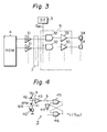
- Figure 3 illustrates a schematic circuit used for effecting data dump operation and extracted from the structure of Fig. 1.
- Fig. 3 shows ROM 4, sense amplifiers 31 corresponding to respective bits, dump enable flag 3, I/O port 6, common bus 7, and output terminals 34 of each bit.
- I/O port 6 comprises AND gates 32 and output buffer amplifiers 33 corresponding to the respective bits.
- Dump enable flag 3 has, for example, a structure as shown in Fig. 4.
- Dump enable flag 3 comprises n-channel type floating gate avalanche injection type MOS (FAMOS) transistor 40, MOS transistors 41 and 42, inverters 23 and 24, and NOR gates 25 and 26.
- FMOS floating gate avalanche injection type MOS
- FAMOS transistor 40 If FAMOS transistor 40 is in a turned-off state, the potential of point a is at a high level. Accordingly, in this case, the dump enable signal S DE of point c is maintained at a low level and the data dumping operation becomes impossible. Therefore, when FAMOS transistor 40 is irradiated with ultraviolet rays, if ROM 4 (Fig. 2) is an EPROM by FAMOS, the content of ROM 4 is erased and FAMOS transistor 40 is simultaneously turned on, so that the data dump operation becomes possible. In the microcomputer according to the present invention, the necessary programs and data are written in ROM 4, which has been irradiated with ultraviolet rays in advance, and confirmation of the operation and debugging are completed.
- transistor 41 is rendered nonconductive, i.e., is turned off, by maintaining gate signal R/W of transistor 41 at a low potential level, and writein of FAMOS transistor 40 is performed by applying a high voltage singal WR to the drain of FAMOS transistor 40 to render said transistor nonconductive. Accordingly, point a is turned to a high potential level and, therefore, the dump enable signal S DE from dump enable flag 3 is turned to a low level and the data dump operation is inhibited.
- a fuse made, for example, of a polycrystalline silicon may be used instead of FAMOS transistor 40 shown in Fig. 4.
- a large current is caused to flow through this fuse so as to break the fuse, thereby rendering the data dump operation.
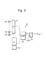
- FIG. 5 illustrates another example of dump enable flag 3 used in the microcomputer according to the present invention.
- the dump enable flag 3 shown in Fig. 5 comprises secret code ROM 50 for storing a secret code determined for each user, input registor 51, secret code input terminals 52, clock signal input terminal 53, a coincidence detecting circuit, i.e., comparator circuit 54, and RS flip-flop 55.
- a clock signal is applied to clock signal input terminal 53 and a secret code is input from secret code input terminals 52.
- the secret code is stored in input register 51.
- the comparator circuit 54 compares the secret code stored in input register 51 with the secret code read out from secret code ROM 50. When these secret codes match, the comparator circuit 54 outputs a high level signal (point d).
- RS flip-flop 55 is reset simultaneously with application of an operating power supply voltage to the microcomputer by a power-on reset signal POR generated from a power-on reset circuit (not shown) and outputs a low level dump enable signal S DE (point c.) If the secret codes match in this state, as mentioned above, since the potential at point d is high, RS flip-flop 55 is set. Therefore, the dump enable signal becomes high and it is possible to effect the data dump operation. On the contrary, if the secret codes do not match, the potential of point d becomes low, and RS flip-flop 55 is not set, so that the dump enable signal S DE (point c) is maintained at a low level. Therefore, in this case, the data dump operation becomes impossible.
- the secret code may be inputted through a data bus or an address bus, and the signal system of the secret codes may be a series, parallel, or series-parallel system.
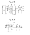
- Figure 6A illustrates a dump circuit which is used in a microcomputer as another embodiment of the present invention and in which dumped data outputs are camouflaged to render it impossible to decode them.
- the circuit shown in Fig. 6A comprises PLA 60 inserted in a readout data line from ROM 4 and changes the sequence of the dumped data outputs or converts them into secret data consisting of a combination of noninverted data and inverted data of the originally readout signals from ROM 4.
- PLA 60 is provided with various gates and inverters and converts input data to secret data according to a predetermined rule, that is, renders it impossible to decode the dumped output data.
- Figure 6B illustrates an example of the above-mentioned circuit of PLA 60.
- PLA 60 of Fig. 6B comprises a plurality of inverters 61 and a route-designating ROM (not shown).
- the content of the route-designating ROM determines whether or not each of inverters 61 is inserted into a respective one of the data lines. Therefore, if a user designates inversion or noninversion for each bit, information corresponding to this designation is written in said ROM.
- the dumped data outputs are camouflaged.
- the operation of the data dump means can be inhibited or the dumped data output or dump address input can be camouflaged, third persons cannot learn the stored content of the built-in memory, such as a ROM. Therefore, it becomes impossible for third persons to imitate the product using the microcomputer according to the present invention.
- the ROM for storing data and programs and the ROM in the dump enable flag are comprised of EPROM's
- the adjacent disposition of the EPROM's on a semiconductor chip makes it impossible to change the content of only the ROM in the dump enable flag. Therefore, imitation of the products using the microcomputer can be surely prevented.
Applications Claiming Priority (2)
| Application Number | Priority Date | Filing Date | Title |
|---|---|---|---|
| JP45625/81 | 1981-03-30 | ||
| JP56045625A JPS57161946A (en) | 1981-03-30 | 1981-03-30 | Microcomputer with protecting mechanism for memory contents |
Publications (2)
| Publication Number | Publication Date |
|---|---|
| EP0062438A2 true EP0062438A2 (fr) | 1982-10-13 |
| EP0062438A3 EP0062438A3 (fr) | 1984-09-05 |
Family
ID=12724545
Family Applications (1)
| Application Number | Title | Priority Date | Filing Date |
|---|---|---|---|
| EP82301475A Withdrawn EP0062438A3 (fr) | 1981-03-30 | 1982-03-23 | Micro-ordinateur avec moyens de protection du contenu de mémoire |
Country Status (2)
| Country | Link |
|---|---|
| EP (1) | EP0062438A3 (fr) |
| JP (1) | JPS57161946A (fr) |
Cited By (12)
| Publication number | Priority date | Publication date | Assignee | Title |
|---|---|---|---|---|
| EP0137995A2 (fr) * | 1983-10-14 | 1985-04-24 | Kabushiki Kaisha Toshiba | Micro-ordinateur monopuce ayant une fonction chiffrable de sa mémoire de programmes |
| EP0145405A2 (fr) * | 1983-12-05 | 1985-06-19 | International Electronic Technology Corporation | Dispositif de sécurité pour équipement électronique commandé par microprocesseur |
| EP0151049A2 (fr) * | 1984-02-02 | 1985-08-07 | National Research Development Corporation | Micro-ordinateur à protection de logiciel |
| EP0154252A2 (fr) * | 1984-02-23 | 1985-09-11 | Fujitsu Limited | Dispositif à mémoire morte programmable et système de mémoire l'utilisant |
| EP0175487A2 (fr) * | 1984-08-23 | 1986-03-26 | Btg International Limited | Dispositif de protection de logiciel |
| GB2165377A (en) * | 1984-09-19 | 1986-04-09 | Itt Ind Ltd | A computer element |
| EP0287338A2 (fr) * | 1987-04-15 | 1988-10-19 | Rohm Corporation | Circuit de sécurité pour réseau logique programmable |
| US5682031A (en) * | 1991-05-06 | 1997-10-28 | Gemplus Card International | Smart card and smart card locking process therefor |
| GB2330932A (en) * | 1997-10-15 | 1999-05-05 | Dell Usa Lp | Method and system for preventing unauthorized access to a computer program |
| WO2005043301A2 (fr) * | 2003-10-24 | 2005-05-12 | Intel Corporation | Debogage d'un composant de confiance dans un systeme |
| WO2006120702A1 (fr) * | 2005-05-09 | 2006-11-16 | Trinity Future-In Pvt. Ltd, | Systeme electromecanique pour une non duplication du systeme d’exploitation |
| WO2007013091A1 (fr) * | 2005-07-25 | 2007-02-01 | Trinity Future-In Pvt. Ltd | Système électromécanique empêchant la duplication de logiciels |
Families Citing this family (3)
| Publication number | Priority date | Publication date | Assignee | Title |
|---|---|---|---|---|
| JPS59226961A (ja) * | 1983-06-08 | 1984-12-20 | Nec Corp | マイクロプロセツサ |
| JPS6011931A (ja) * | 1983-06-30 | 1985-01-22 | Fujitsu Ltd | ワンチツプマイクロコンピユ−タ |
| JPH021019A (ja) * | 1988-12-02 | 1990-01-05 | Hitachi Ltd | 1チップマイクロコンピュータ |
Citations (3)
| Publication number | Priority date | Publication date | Assignee | Title |
|---|---|---|---|---|
| US3971916A (en) * | 1974-03-25 | 1976-07-27 | Societe Internationale | Methods of data storage and data storage systems |
| FR2401459A1 (fr) * | 1977-08-26 | 1979-03-23 | Cii Honeywell Bull | Support d'information portatif muni d'un microprocesseur et d'une memoire morte programmable |
| US4168396A (en) * | 1977-10-31 | 1979-09-18 | Best Robert M | Microprocessor for executing enciphered programs |
-
1981
- 1981-03-30 JP JP56045625A patent/JPS57161946A/ja active Pending
-
1982
- 1982-03-23 EP EP82301475A patent/EP0062438A3/fr not_active Withdrawn
Patent Citations (3)
| Publication number | Priority date | Publication date | Assignee | Title |
|---|---|---|---|---|
| US3971916A (en) * | 1974-03-25 | 1976-07-27 | Societe Internationale | Methods of data storage and data storage systems |
| FR2401459A1 (fr) * | 1977-08-26 | 1979-03-23 | Cii Honeywell Bull | Support d'information portatif muni d'un microprocesseur et d'une memoire morte programmable |
| US4168396A (en) * | 1977-10-31 | 1979-09-18 | Best Robert M | Microprocessor for executing enciphered programs |
Non-Patent Citations (1)
| Title |
|---|
| IBM TECHNICAL DISCLOSURE BULLETIN, vol. 19, no. 11, April 1977, page 4241, New York, US * |
Cited By (24)
| Publication number | Priority date | Publication date | Assignee | Title |
|---|---|---|---|---|
| EP0137995A2 (fr) * | 1983-10-14 | 1985-04-24 | Kabushiki Kaisha Toshiba | Micro-ordinateur monopuce ayant une fonction chiffrable de sa mémoire de programmes |
| EP0137995A3 (en) * | 1983-10-14 | 1987-12-16 | Kabushiki Kaisha Toshiba | Single-chip microcomputer with encryptable function on program memory |
| EP0145405A3 (en) * | 1983-12-05 | 1987-07-08 | International Electronic Technology Corporation | Security arrangement for microprecessor-controlled electronic equipment |
| EP0145405A2 (fr) * | 1983-12-05 | 1985-06-19 | International Electronic Technology Corporation | Dispositif de sécurité pour équipement électronique commandé par microprocesseur |
| EP0151049A2 (fr) * | 1984-02-02 | 1985-08-07 | National Research Development Corporation | Micro-ordinateur à protection de logiciel |
| EP0151049A3 (fr) * | 1984-02-02 | 1989-07-26 | National Research Development Corporation | Micro-ordinateur à protection de logiciel |
| EP0154252A3 (en) * | 1984-02-23 | 1989-08-30 | Fujitsu Limited | Programmable read only memory device and memory system employing the same |
| EP0154252A2 (fr) * | 1984-02-23 | 1985-09-11 | Fujitsu Limited | Dispositif à mémoire morte programmable et système de mémoire l'utilisant |
| EP0175487A3 (fr) * | 1984-08-23 | 1989-03-08 | Btg International Limited | Dispositif de protection de logiciel |
| EP0175487A2 (fr) * | 1984-08-23 | 1986-03-26 | Btg International Limited | Dispositif de protection de logiciel |
| GB2165377A (en) * | 1984-09-19 | 1986-04-09 | Itt Ind Ltd | A computer element |
| EP0287338A2 (fr) * | 1987-04-15 | 1988-10-19 | Rohm Corporation | Circuit de sécurité pour réseau logique programmable |
| EP0287338A3 (en) * | 1987-04-15 | 1989-07-19 | Exel Microelectronics, Inc. | Security fuse circuit for programmable logic array |
| US5682031A (en) * | 1991-05-06 | 1997-10-28 | Gemplus Card International | Smart card and smart card locking process therefor |
| US6237137B1 (en) | 1997-10-15 | 2001-05-22 | Dell Usa, L.P. | Method and system for preventing unauthorized access to a computer program |
| GB2330932A (en) * | 1997-10-15 | 1999-05-05 | Dell Usa Lp | Method and system for preventing unauthorized access to a computer program |
| AU736077B2 (en) * | 1997-10-15 | 2001-07-26 | Dell Usa L.P. | Method and system for preventing unauthorized access to a computer program |
| GB2330932B (en) * | 1997-10-15 | 2002-06-26 | Dell Usa Lp | Method and system for preventing unauthorized access to a computer program |
| WO2005043301A2 (fr) * | 2003-10-24 | 2005-05-12 | Intel Corporation | Debogage d'un composant de confiance dans un systeme |
| WO2005043301A3 (fr) * | 2003-10-24 | 2006-05-04 | Intel Corp | Debogage d'un composant de confiance dans un systeme |
| US7321957B2 (en) | 2003-10-24 | 2008-01-22 | Intel Corporation | Debugging a trusted component in a system |
| WO2006120702A1 (fr) * | 2005-05-09 | 2006-11-16 | Trinity Future-In Pvt. Ltd, | Systeme electromecanique pour une non duplication du systeme d’exploitation |
| WO2007013091A1 (fr) * | 2005-07-25 | 2007-02-01 | Trinity Future-In Pvt. Ltd | Système électromécanique empêchant la duplication de logiciels |
| US8079092B2 (en) | 2005-07-25 | 2011-12-13 | M/s. Trinity Future—In PVT. Ltd. | Electro-mechanical system for non-duplication of software |
Also Published As
| Publication number | Publication date |
|---|---|
| EP0062438A3 (fr) | 1984-09-05 |
| JPS57161946A (en) | 1982-10-05 |
Similar Documents
| Publication | Publication Date | Title |
|---|---|---|
| US4513389A (en) | ROM security circuit | |
| EP0062438A2 (fr) | Micro-ordinateur avec moyens de protection du contenu de mémoire | |
| US4796235A (en) | Write protect mechanism for non-volatile memory | |
| US5036486A (en) | Associative memory device | |
| KR950014560B1 (ko) | 불휘발성 기억 장치 | |
| US5224070A (en) | Apparatus for determining the conditions of programming circuitry used with flash EEPROM memory | |
| KR940005784B1 (ko) | 보안회로 | |
| KR101110994B1 (ko) | 에러 동작으로부터 집적 회로를 보호하는 방법 및 장치 | |
| EP0287338B1 (fr) | Circuit de sécurité pour réseau logique programmable | |
| KR890004999B1 (ko) | 프로그램 가능 판독 전용 메모리장치 및 그를 이용한 메모리시스템 | |
| US6135651A (en) | Patching apparatus and method for upgrading modem software code | |
| US5809544A (en) | Microcontroller which limits access to internal memory | |
| US5047989A (en) | Chapter mode selection apparatus for MOS memory | |
| US4893281A (en) | Semiconductor memory system with programmable address decoder | |
| JP2001084780A (ja) | 不揮発性半導体記憶装置 | |
| US4580217A (en) | High speed memory management system and method | |
| JPH07319765A (ja) | 半導体集積回路 | |
| US5642480A (en) | Method and apparatus for enhanced security of a data processor | |
| US5062075A (en) | Microcomputer having security memory using test and destruction routines | |
| US6324626B1 (en) | Semiconductor memory | |
| US5101376A (en) | Integrated microprocessor with associative memory device | |
| US5355336A (en) | Memory device and a method for prohibiting writing to the memory device | |
| US5892711A (en) | Sector protection circuit for a flash memory device | |
| JPH03204053A (ja) | 読出し専用メモリ | |
| JPS59140695A (ja) | 半導体集積回路装置 |
Legal Events
| Date | Code | Title | Description |
|---|---|---|---|
| PUAI | Public reference made under article 153(3) epc to a published international application that has entered the european phase |
Free format text: ORIGINAL CODE: 0009012 |
|
| AK | Designated contracting states |
Designated state(s): DE FR GB NL |
|
| PUAL | Search report despatched |
Free format text: ORIGINAL CODE: 0009013 |
|
| AK | Designated contracting states |
Designated state(s): DE FR GB NL |
|
| 17P | Request for examination filed |
Effective date: 19841019 |
|
| STAA | Information on the status of an ep patent application or granted ep patent |
Free format text: STATUS: THE APPLICATION IS DEEMED TO BE WITHDRAWN |
|
| 18D | Application deemed to be withdrawn |
Effective date: 19861216 |
|
| RIN1 | Information on inventor provided before grant (corrected) |
Inventor name: SUZUKI, TETSUO |