EP0060992A2 - Maquette d'essai et circuit d'évaluation pour détecteur de proximité à commande de machines - Google Patents
Maquette d'essai et circuit d'évaluation pour détecteur de proximité à commande de machines Download PDFInfo
- Publication number
- EP0060992A2 EP0060992A2 EP82101038A EP82101038A EP0060992A2 EP 0060992 A2 EP0060992 A2 EP 0060992A2 EP 82101038 A EP82101038 A EP 82101038A EP 82101038 A EP82101038 A EP 82101038A EP 0060992 A2 EP0060992 A2 EP 0060992A2
- Authority
- EP
- European Patent Office
- Prior art keywords
- circuit
- proximity switch
- output signal
- rel
- transformer
- Prior art date
- Legal status (The legal status is an assumption and is not a legal conclusion. Google has not performed a legal analysis and makes no representation as to the accuracy of the status listed.)
- Granted
Links
Images

Classifications
-
- H—ELECTRICITY
- H03—ELECTRONIC CIRCUITRY
- H03K—PULSE TECHNIQUE
- H03K17/00—Electronic switching or gating, i.e. not by contact-making and –breaking
- H03K17/94—Electronic switching or gating, i.e. not by contact-making and –breaking characterised by the way in which the control signals are generated
- H03K17/945—Proximity switches
Definitions
- the invention relates to a test and evaluation circuit for a testable proximity switch provided as an electrical element of a machine control.
- proximity switches as elements of machine controls for monitoring movable parts, which can be checked for their functionality, specifically inductive or capacitive proximity switches, in which an electrically periodically switchable damping circuit is provided for checking the functionality, with the aid of an oscillator can be damped, which contains an inductive or capacitive control element.
- the damping circuit essentially consists of a pushbutton, by means of which a part of a winding of an inductive proximity switch can be short-circuited, whereby it was also considered to actuate the damping circuit periodically in order to check it at certain intervals of the proximity switch on its functionality.
- the invention was therefore based on the object, based on the earlier proposal, of specifying an improved test and evaluation circuit for testable proximity switches, which permits continuous monitoring of the trouble-free operation of the proximity switch itself and of the elements of the test and evaluation circuit.
- a control circuit is provided by which the proximity switch can be reversed between its two switching states for generating a clocked output signal with a predetermined frequency
- an evaluation circuit is provided, by means of which an enable signal can be generated for the duration of the presence of a clocked output signal of the proximity switch, and a blocking signal for the machine control can be generated if there are no potential changes in the output signal of the proximity switch.
- the proximity switch opens up the possibility of supplying the output signal of the proximity switch, which is present in the form of an alternating voltage or a square-wave pulse sequence and which can be obtained in the case of an optical proximity switch, for example by clocked switching on and off of a light transmitter, via a transformer, whereby only the The fact that a continuous signal is transmitted via the transformer already indicates that the proximity switch located in front of the transformer works with its associated astable multivibrator without any loss.
- a proximity switch according to the invention which has an inductive probe containing a probe coil in the oscillating circuit of the oscillator in a manner known per se, it has proven to be advantageous if a short circuit can be at least partially brought about for the probe coil in the one switching position of the multivibrator , It is particularly advantageous in the case of a probe coil with a tap if a short circuit can be brought about by the multivibrator for a winding part of the probe coil lying between the tap and one of the outer connections.
- a short circuit can be brought about directly for the probe coil or its winding part by means of a switching transistor connected in parallel and controllable by the multivibrator. It is particularly advantageous if a defined series resistance is inserted in the short circuit.
- the output of the proximity switch is connected to the input of a control circuit, the output of which is connected via a transformer to the input of a relay circuit which contains two relays, each as elements of a machine start-up control have a make contact, and when the make contacts are inserted in series with each other in the main contact path of the machine circuit.
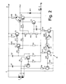
- FIG. 1 shows a testable proximity switch 8, in which a control circuit 10 is integrated in the exemplary embodiment, as is indicated by a block shown in dashed lines, by means of which a damping circuit of the proximity switch 8 can be switched on and off periodically.
- the proximity switch 8 has an output A, which is connected to the input of a drive circuit 12, which in the exemplary embodiment is composed of an amplifier 18 and an inverting amplifier 20, the inverting amplifier 20 in the event of a malfunction of the proximity switch 8 or a damping thereof blocks a first output potential of the proximity switch 8 as well as the first amplifier 18 at a second potential at the output A of the proximity switch 8.
- the outputs of the two amplifiers 18, 20 are connected to a transformer Tr, the primary winding of which in the execution. 1 is designed as a winding with a center tap.
- the secondary winding of the transformer Tr is connected to the input of a relay circuit 14, which as essential elements has two relays Rel 1 and Rel 2, each of which has a normally open contact inserted into a main contact path 16 of a machine control, as will be explained further below with reference to FIG. 4 will be explained in detail.
- a relay circuit 14 which as essential elements has two relays Rel 1 and Rel 2, each of which has a normally open contact inserted into a main contact path 16 of a machine control, as will be explained further below with reference to FIG. 4 will be explained in detail.
- Fig. 1 connected to the output A of the proximity switch 8 associated formwork do g s or circuit parts of an evaluation circuit 9, which is associated with 20, a power supply or a power supply that is fed from the well, the proximity switch 8 itself.
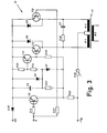
- the proximity switch to be tested according to the invention is first and foremost a largely customary inductive proximity switch.
- This proximity switch has a probe coil L on the input side, which is usually arranged in a pot core which is open towards the front - that is, towards the moving parts to be monitored.
- the probe coil L has external connections 2, 3 which are connected to the supply connection 6 of the proximity switch or to the emitter of the transistor T 1.
- Parallel to the probe coil L is a capacitor C 1, which together with the probe coil L forms an oscillating circuit L, C 1.
- the oscillator of the proximity switch 8 according to FIG. 2 also has two transistors T 1 and T 2 and three resistors Rx, R 1 and R 2.
- the base connections of the transistors T 1 ' and T 2 are connected to the connection 4 of the proximity switch via the resistor R 1.
- the emitter of the transistor T 1 is connected on the one hand to the outer terminal 2 of the probe coil L and on the other hand to the capacitor C 1.
- the collector of the transistor T 1 is not connected, so that only the base-emitter path of the transistor T 1 is effective as a diode, but this diode's electrical properties can be matched particularly precisely to the properties of the transistor T 2, the Collector is connected via resistor R 2 to terminal 4 and its emitter is connected via resistor Rx to terminal 1 of proximity switch 8, that is, with a tap of probe coil L, which is divided into two partial windings L 1 and L 2 by these taps .
- a flip-flop circuit is connected to the oscillator described above, which has a capacitor C 2, resistors R 3 to R 11 and two further transistors T 3 and T 4, the capacitor C 2 also being part of the oscillator.
- the capacitor C 2 is connected on the one hand to the terminal 6 of the proximity switch and on the other hand to the collector of the transistor T 2.
- resistor R 2 and capacitor C 2 a resistor R 3 is connected to the base of transistor T 3 of the trigger circuit.
- the emitter of this transistor T 3, which is designed as a Pnp transistor, is connected on the one hand via resistor R 4 to terminal 4 and on the other hand via resistor R 5 to terminal 6 of the proximity switch.
- the collector of transistor T 3 is connected to the base of transistor T 4 via resistor R 7.
- the base of transistor T 4 is also connected to terminal 6 via resistor R 6, while the emitter of transistor T 4 is connected directly to terminal 6.
- the collector of the transistor T 4 is connected via the resistor R 8 to the base of the transistor T 3 and via the resistors R 9 to R 11 to the terminal 4 and forms a terminal which connects the output A of the trigger circuit or the input to it connected control circuit 12 forms.
- the probe coil L is normally located in a shell core which is open towards the front, so that a magnetic field with a large spread can be built up. If a metal part M is now moved into this field, induced eddy currents flow in it, which draw energy from the field. These eddy current losses cause a deterioration in the quality of the oscillating circuit, so that the oscillation amplitude is reduced. In other words, the resonant circuit is damped.
- the elements R 2, T 2, Rx and L 1 form a voltage divider for the duration of the negative half-wave of the oscillation.
- a comparatively high negative voltage arises at the collector of the transistor T 2, because the resistance R 2 has a high resistance to the other elements of the voltage divider. The result of this is that the capacitor C 2 is charged only slightly at the input of the trigger circuit. If the transistor T 2 then blocks during the positive half-wave of the oscillation, then the capacitor C 2 continues to charge slightly via the resistor R 2 until the next negative half-cycle of the oscillation occurs.
- the capacitor C 2 thus smoothes the voltage at the collector of the transistor T 2 or at the input of the trigger circuit in such a way that a DC voltage with negligible residual ripple results.
- This voltage is so high or so close to OV that the transistor T 3 is turned on, so that the transistor T 4 and a resistor R 12 connected to its collector are connected Transistor T 6 are controlled conductive. Since the emitter of the transistor T 6 is connected to the terminal 4 via a diode D 3, the output A of the proximity switch, namely the collector of the transistor T 6, has a positive potential (+ U B ) compared to the terminal 6 Zener diode ZD 1 in parallel to transistor T 6 protects this transistor and limits interference voltage peaks.
- transistor T 5 Parallel to the base-emitter path of transistor T 6 there is also a transistor T 5, the base of which is connected to the common connection point of resistors R 10 and R 11, which in turn is connected in series with resistor R 9 between the collector of transistor T. 4 and the terminal 4 of the proximity switch 8 are.
- the common connection point of the resistors R 9 and R 10 is connected via a diode D 1 to the collector of the transistor T 6, which is also connected to the terminal 6 via the series circuit of a further diode D 2 and a resistor R 13.
- the capacitor C 2 charges up to a higher voltage, the voltage level being exceeded which is required in order to flip the trigger circuit into the off state.
- the emitter potential of the transistor T 3 is essentially determined by the resistors R 4 and R 5, in such a way that the switch-off threshold or the switch-on threshold essentially corresponds to the emitter potential, if the voltage drop at R 3 and the base-emitter voltage U BE are neglected.
- the voltage rise across the capacitor C 2 thus blocks the transistor T 3, as a result of which the downstream transistors T 4 and T 6 are also switched to the non-conductive state, since they can no longer be supplied with a base current.
- the level of the output signal at the output A of the proximity switch 8 practically drops to the value of OV.
- a proximity switch of the type under consideration in which the resistance Rx is used to individually adjust the response distance between the active surface of the probe and the movable element to be monitored, is used to monitor safety devices on machines, a defect can have disastrous consequences. No damage is possible if damping is simulated and a relay controlled by the proximity switch drops out, since in this case a machine fault is simulated and the machine cannot start or is stopped. However, if a vibration is simulated in spite of the damping actually being present, which is the case, for example, when the transistors T 3, T 4 or T 6 break down, the machine can start up despite the fault, which may result in serious damage to property or even personal injury .
- the proximity switch 8 or the oscillator has already been proposed to assign a damping circuit to it, with which damping of the oscillator can be brought about for test purposes, if necessary periodically, to check whether such damping actually results in a signal change at the output of the proximity switch, such a signal change indicating the functionality of the proximity switch.
- a control circuit 10 is now assigned to the proximity switch 8, which can be integrated into the proximity switch itself, but which can also be combined with the other elements of the test and monitoring circuit according to the invention at a distance from the actual proximity switch.
- the control circuit is designed as an astable multivibrator 10.
- this astable multivibrator consists of resistors R 17 to R 20, capacitors C 4 and C 5 and transistors T 8, T 9 and diodes D 4 and D 5. Due to the circuit structure shown in FIG the multivibrator 10 a safe when switching on the operating voltage Swinging guaranteed, the diodes D 4 and D 5 serve to protect the base connections of the transistors T 8, T 9 against negative voltage peaks, such as occur in the switching moment.
- the collector of the transistor T 8 forms the output of the circuit via which the actual damping circuit with the transistor T 7 and the resistor R 14 connected in series can be controlled, this series circuit comprising the resistor R 14 and the transistor T 7 is parallel to the probe connections 1 and 3 and thus to the partial winding L 1, which can consequently be short-circuited.
- This short-circuiting of the partial winding L 1 takes place, for example, at a clock frequency of 140 Hz and simulates damping of the oscillator of the proximity switch 8, at the output A of which a clocked or a dynamic output signal is thus available.
- the transistor T 10 If the signal has its low level (OV), the transistor T 10 is blocked, while the transistor T 12 can receive a base current via the resistors R 22 and R 26 and is thus controlled to be conductive. A current now flows from the positive connection terminal (+ U B ) via the PTC thermistor R 29 through the partial winding W 1 of the transformer Tr and via the conductive transistor T 12 to the other connection (OV) of the circuit.
- the transistors T 10 and T 13 are turned on, while the transistor T 12 blocks.
- the current now flows from the positive terminal + U B via the PTC thermistor R 29 through the partial winding W 2 and the transistor T 13 to the other connection of the circuit.
- a partial current flows through the partial windings W 1 and W 2 of the primary winding of the transformer Tr alternately.
- the proximity switch 8 is now damped, for example, at a time t by a metal part M which is brought close enough, then a static signal of low level results at its output, while the potential changes also occur at the collectors of the transistors T 10 and T 13 according to FIG. 5b stop and a high level static signal appears. If this static state persists for a longer period of time, the transistor T 12 could be thermally overloaded because the current through this transistor is only limited by the low DC resistance of the partial winding w 1.
- the transistor T 12 must therefore be switched off by a time function, which happens in the exemplary embodiment in such a way that the resistors R 22 and R 23 charge the capacitor C 6 after an e-function until a voltage is present across the capacitor C 6 , which is sufficient to conductively control the transistor T 11 via the tap of the voltage divider R 24, R 25. Once this is ge happens, the base of the transistor T 12 is switched to the potential OV, so that the transistor T 12 blocks.
- the components C 6, R 23, R 24 and R 25 are dimensioned in such a way that the transistor T 12 is switched off or off after a time interval a, as is clear from FIG. 5c, where the voltage curve across the capacitor C 6 is shown. It can be seen that the duration of the time interval a corresponds approximately to twice the duty cycle of the dynamic output signal of the proximity switch.
- the transformer Tr and the relay circuit 14 If the input E of the evaluation circuit 9 is accidentally connected to the control circuit 12, the transformer Tr and the relay circuit 14 with the positive operating voltage, this can result in a thermal overload of the transistor T 13 in a corresponding manner.
- the PTC thermistor R 29 is inserted into the connection to be connected to the positive supply voltage + U B , the response time of which is approximately 3 to 4 seconds if a partial winding w 1 or w 2 of the primary winding of the transformer Tr is continuously supplied by a direct current is flowed through and is dimensioned so that the switching transistor T 13 and the transformer Tr are protected against inadmissible heating.
- the cold conductor R 29 must first cool down for a time interval of approximately 30 to 40 seconds until the circuit can resume normal operation. Otherwise, the voltage curve on the collector of transistor T 12 is shown in FIG. 5d, while the voltage curve on the secondary side of transformer Tr is shown in FIG. 5e.
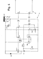
- the connections of the secondary winding w 3 of the transformer Tr are connected to a bridge rectifier B, via which the relay circuit 14 is supplied.
- the positive output terminal of the bridge rectifier B is connected to the one terminal of a first relay Rel 1, the second terminal of which is connected via normally closed contacts 2d and 2c of a second relay Rel 2 to the negative terminal of the rectifier B. With this negative connection, the second connection of the relay Rel 1 can also be connected via one of its working contacts 1f.
- the first terminal of the second relay Rel 2 is also connected to the positive output of the bridge rectifier B, while the second terminal of the second relay Rel 2 via the switching path of a T hrystors Th to the negative terminal of the bridge rectifier B is connected.
- the control electrode of the thyristor Th is connected on the one hand via a resistor R 32 to the negative terminal of the bridge rectifier B and on the other hand via the series circuit of a resistor R 31 and a normally open contact 1d of the first relay Rel 1 with the connection point of the resistor R 30 and the capacitor C.
- the two relays are now not simply connected in parallel according to the invention, since in this case no warning signal could be generated if one of the relays gets stuck, so that ultimately a similarly low level of safety would be achieved as if only one relay were used. Rather, the two relays Rel 1 and Rel 2 are switched in the relay circuit 14 according to the invention in such a way that they monitor one another, that is to say in such a way that an error message is triggered even if only one of the two relays gets stuck, in which case the Main contact path 16 of the machine control with the work contacts 1a and 2a of relays Rel 1 and Rel 2 remains interrupted.
- a test and monitoring circuit which is not only suitable for continuously monitoring the functionality of a testable proximity switch, but which is also constructed in such a way that using the dynamic output signal of the interference-free working proximity switch is also a self-monitoring of all essential circuit components of the monitoring circuit.
- extremely high security is achieved for the release and blocking of the machine control connected to the proximity switch, as is clear from the following list of possible errors in the relay circuit, in which the individual components are only identified by their reference numerals and in which Abbreviation HKS is used to designate the main contact section 16.
- the proximity switch is used as an opener or a closer and whether the Proximity switch is normally damped or damped or activated or not activated.
Applications Claiming Priority (2)
| Application Number | Priority Date | Filing Date | Title |
|---|---|---|---|
| DE3110390 | 1981-03-18 | ||
| DE19813110390 DE3110390A1 (de) | 1981-03-18 | 1981-03-18 | Pruef- und auswerteschaltung fuer naeherungsschalter in maschinensteuerungen |
Publications (3)
| Publication Number | Publication Date |
|---|---|
| EP0060992A2 true EP0060992A2 (fr) | 1982-09-29 |
| EP0060992A3 EP0060992A3 (en) | 1982-12-29 |
| EP0060992B1 EP0060992B1 (fr) | 1987-01-07 |
Family
ID=6127553
Family Applications (1)
| Application Number | Title | Priority Date | Filing Date |
|---|---|---|---|
| EP82101038A Expired EP0060992B1 (fr) | 1981-03-18 | 1982-02-12 | Maquette d'essai et circuit d'évaluation pour détecteur de proximité à commande de machines |
Country Status (4)
| Country | Link |
|---|---|
| US (1) | US4492925A (fr) |
| EP (1) | EP0060992B1 (fr) |
| JP (1) | JPS57161668A (fr) |
| DE (2) | DE3110390A1 (fr) |
Cited By (5)
| Publication number | Priority date | Publication date | Assignee | Title |
|---|---|---|---|---|
| EP0132850A1 (fr) * | 1983-07-28 | 1985-02-13 | Gebhard Balluff Fabrik feinmechanischer Erzeugnisse GmbH & Co. | Commutateur de proximité auto-contrôlé |
| GB2177216A (en) * | 1985-07-05 | 1987-01-14 | Baumer Electric Ag | Proximity switch |
| EP0308766B1 (fr) * | 1987-09-24 | 1991-11-27 | Siemens Aktiengesellschaft | Commutateur de proximité avec circuits de test et d'évaluation |
| US10685800B2 (en) | 2018-06-18 | 2020-06-16 | Edward W. Anderson | Testable sealed relay and self-diagnosing relay |
| CN115327372A (zh) * | 2022-10-18 | 2022-11-11 | 山东天大清源信息科技有限公司 | 一种接近开关动作频率检测装置 |
Families Citing this family (12)
| Publication number | Priority date | Publication date | Assignee | Title |
|---|---|---|---|---|
| DE3220111C1 (de) * | 1982-05-28 | 1983-06-09 | Honeywell Gmbh, 6050 Offenbach | Überwachungseinrichtung für Näherungsschalter |
| DE3331784A1 (de) * | 1983-09-02 | 1985-03-21 | J. Wagner Gmbh, 7990 Friedrichshafen | Einrichtung zum behandeln von hohlraeumen |
| FR2559305B1 (fr) * | 1984-02-08 | 1986-10-17 | Telemecanique Electrique | Manipulateur analogique |
| JPS6114501A (ja) * | 1984-06-30 | 1986-01-22 | Nippon Kokan Kk <Nkk> | 渦流式距離計 |
| DE3505765A1 (de) * | 1985-02-20 | 1986-08-21 | Werner Turck Gmbh & Co Kg, 5884 Halver | Induktiver naeherungsschalter mit pruefeinrichtung |
| DE3903278C2 (de) * | 1989-02-03 | 1995-09-28 | Rexroth Mannesmann Gmbh | Induktive Wegaufnehmeranordnung |
| DE3909613A1 (de) * | 1989-03-23 | 1990-09-27 | Hans Turck Gmbh & Co Kg | Schaltungsanordnung zur selbstueberwachung eines schaltgeraetes fuer einen lastkreis |
| US5029188A (en) * | 1989-11-03 | 1991-07-02 | Joyner Engineers And Trainers | Apparatus for monitoring operation cycles of an electrically actuated device |
| AT412636B (de) * | 2000-02-23 | 2005-05-25 | Vae Eisenbahnsysteme Gmbh | Einrichtung zur überwachung und prognose der ausfallwahrscheinlichkeit von induktiven näherungssensoren |
| JP3811454B2 (ja) * | 2003-01-29 | 2006-08-23 | インターナショナル・ビジネス・マシーンズ・コーポレーション | 近接検出装置、ポータブルコンピュータ、近接検出方法、及びプログラム |
| DE10329975B4 (de) * | 2003-06-26 | 2005-05-12 | Siemens Ag | Verfahren und Vorrichtung zur Funktionsprüfung eines induktiven Sensors |
| DE102009046737B4 (de) * | 2009-11-16 | 2016-08-04 | Balluff Gmbh | Sensorvorrichtung, Programmiervorrichtung, Kombination aus Sensorvorrichtung und Programmiervorrichtung |
Citations (4)
| Publication number | Priority date | Publication date | Assignee | Title |
|---|---|---|---|---|
| DE2150694B2 (de) * | 1971-10-12 | 1976-05-20 | Klaschka, Walter, Dr.-Ing., 7531 Tiefenbronn | Beruehrungsloser sicherheitsschalter |
| DE2166021B2 (de) * | 1971-08-10 | 1978-01-05 | Ausscheidung aus: 21 40 056 Hermle, Eduard, 7303 Neuhausen | Elektronischer naeherungsschalter |
| DE2745650A1 (de) * | 1977-10-11 | 1979-04-12 | Klaschka Ind Elektronik | Annaeherungsschalter |
| EP0035225A2 (fr) * | 1980-03-01 | 1981-09-09 | Gebhard Balluff Fabrik feinmechanischer Erzeugnisse GmbH & Co. | Commutateur de proximitié avec ses dispositifs de surveillance |
Family Cites Families (4)
| Publication number | Priority date | Publication date | Assignee | Title |
|---|---|---|---|---|
| GB2022893B (en) * | 1978-06-10 | 1983-01-12 | Westinghouse Brake & Signal | Fault detection |
| ZA792482B (en) * | 1978-06-10 | 1980-06-25 | Signal Co Ltd | Railway control signal dynamic output interlocking systems |
| DE2921095C2 (de) * | 1979-05-22 | 1983-03-31 | Auergesellschaft Gmbh, 1000 Berlin | Verfahren zur Überwachung des Schaltzustandes von Schaltelementen |
| DE2942134A1 (de) * | 1979-10-18 | 1981-04-30 | Robert Bosch Gmbh, 7000 Stuttgart | Auswerteschaltung fuer einen induktivgeber |
-
1981
- 1981-03-18 DE DE19813110390 patent/DE3110390A1/de not_active Withdrawn
-
1982
- 1982-02-12 EP EP82101038A patent/EP0060992B1/fr not_active Expired
- 1982-02-12 DE DE8282101038T patent/DE3275015D1/de not_active Expired
- 1982-02-26 US US06/352,804 patent/US4492925A/en not_active Expired - Fee Related
- 1982-03-17 JP JP57040981A patent/JPS57161668A/ja active Pending
Patent Citations (4)
| Publication number | Priority date | Publication date | Assignee | Title |
|---|---|---|---|---|
| DE2166021B2 (de) * | 1971-08-10 | 1978-01-05 | Ausscheidung aus: 21 40 056 Hermle, Eduard, 7303 Neuhausen | Elektronischer naeherungsschalter |
| DE2150694B2 (de) * | 1971-10-12 | 1976-05-20 | Klaschka, Walter, Dr.-Ing., 7531 Tiefenbronn | Beruehrungsloser sicherheitsschalter |
| DE2745650A1 (de) * | 1977-10-11 | 1979-04-12 | Klaschka Ind Elektronik | Annaeherungsschalter |
| EP0035225A2 (fr) * | 1980-03-01 | 1981-09-09 | Gebhard Balluff Fabrik feinmechanischer Erzeugnisse GmbH & Co. | Commutateur de proximitié avec ses dispositifs de surveillance |
Cited By (9)
| Publication number | Priority date | Publication date | Assignee | Title |
|---|---|---|---|---|
| EP0132850A1 (fr) * | 1983-07-28 | 1985-02-13 | Gebhard Balluff Fabrik feinmechanischer Erzeugnisse GmbH & Co. | Commutateur de proximité auto-contrôlé |
| WO1985000712A1 (fr) * | 1983-07-28 | 1985-02-14 | Gebhard Balluff Fabrik Feinmechanischer Erzeugniss | Commutateur capacitif a controle automatique |
| GB2177216A (en) * | 1985-07-05 | 1987-01-14 | Baumer Electric Ag | Proximity switch |
| GB2177216B (en) * | 1985-07-05 | 1989-07-19 | Baumer Electric Ag | Proximity switch |
| EP0308766B1 (fr) * | 1987-09-24 | 1991-11-27 | Siemens Aktiengesellschaft | Commutateur de proximité avec circuits de test et d'évaluation |
| US10685800B2 (en) | 2018-06-18 | 2020-06-16 | Edward W. Anderson | Testable sealed relay and self-diagnosing relay |
| US10937615B2 (en) | 2018-06-18 | 2021-03-02 | Edward W. Anderson | Testable sealed relay and self-diagnosing relay |
| CN115327372A (zh) * | 2022-10-18 | 2022-11-11 | 山东天大清源信息科技有限公司 | 一种接近开关动作频率检测装置 |
| CN115327372B (zh) * | 2022-10-18 | 2023-02-17 | 山东天大清源信息科技有限公司 | 一种接近开关动作频率检测装置 |
Also Published As
| Publication number | Publication date |
|---|---|
| US4492925A (en) | 1985-01-08 |
| JPS57161668A (en) | 1982-10-05 |
| DE3275015D1 (en) | 1987-02-12 |
| EP0060992B1 (fr) | 1987-01-07 |
| EP0060992A3 (en) | 1982-12-29 |
| DE3110390A1 (de) | 1982-10-07 |
Similar Documents
| Publication | Publication Date | Title |
|---|---|---|
| EP0060992A2 (fr) | Maquette d'essai et circuit d'évaluation pour détecteur de proximité à commande de machines | |
| DE2724278A1 (de) | Notstromversorgungseinrichtung | |
| EP0136968A2 (fr) | Dispositif de commande pour l'alimentation d'un électro-aimant par un courant d'appel suivi d'un courant de maintien | |
| DE3218583C2 (de) | Schaltervorrichtung zum öffnen und Schließen eines elektrischen Stromkreises mit einer induktiven Last | |
| EP0035225B1 (fr) | Commutateur de proximitié avec ses dispositifs de surveillance | |
| DE3326012C2 (de) | Einzelimpuls-Erzeugungsschaltung | |
| DE2263867A1 (de) | Steuerschaltung fuer thyristoren | |
| DE2050219C3 (de) | Einrichtung zur Steuerung eines Elektromagneten | |
| DE2707455C3 (de) | Elektronischer Überstrom-Schutzschalter | |
| DE2731453C3 (de) | Erdschlußdetektor | |
| DE2019184C3 (de) | Starkstromschalteinrichtung | |
| DE2803847A1 (de) | Fernschalteinrichtung | |
| DE2806294A1 (de) | Einrichtung zur kontrolle des elektrischen leitungszustandes eines elektromechanischen schaltkontakts | |
| DE3737791C2 (fr) | ||
| EP0308766B1 (fr) | Commutateur de proximité avec circuits de test et d'évaluation | |
| DE2735736C3 (de) | Wechselstromschalteinrichtung | |
| DE2809993C3 (de) | Flammenwächterschaltung zur Überwachung einer Brennerflamme | |
| DE3626209A1 (de) | Vorschaltgeraet fuer wenigstens eine entladungslampe | |
| DE3532229A1 (de) | Elektronischer sicherheitstemperaturbegrenzer | |
| DE2210747C3 (de) | Überlastungsschutzanordnung für einen impulsgespeisten Gleichstrommotor | |
| DE3710513A1 (de) | Geregelte hochspannungs-versorgungsschaltung | |
| DE1513571B2 (de) | Gerat zum Überwachen und Anzeigen von Fehlerstromen in zwei elektrischen Leitern und Fehlerstromschutzschalter mit diesem Gerat | |
| DE4116947C2 (de) | Koppelrelaisschaltung | |
| DE2323287C3 (de) | Schaltungsanordnung zum Zünden und Betrieb einer von einer Wechselstromquelle gespeisten Entladungslampe | |
| DE1298555B (de) | Elektronischer Annaeherungsschalter mit einem Oszillator |
Legal Events
| Date | Code | Title | Description |
|---|---|---|---|
| PUAI | Public reference made under article 153(3) epc to a published international application that has entered the european phase |
Free format text: ORIGINAL CODE: 0009012 |
|
| AK | Designated contracting states |
Designated state(s): CH DE FR GB IT SE |
|
| PUAL | Search report despatched |
Free format text: ORIGINAL CODE: 0009013 |
|
| AK | Designated contracting states |
Designated state(s): CH DE FR GB IT LI SE |
|
| 17P | Request for examination filed |
Effective date: 19821130 |
|
| RAP1 | Party data changed (applicant data changed or rights of an application transferred) |
Owner name: GEBHARD BALLUFF FABRIK FEINMECHANISCHER ERZEUGNISS |
|
| GRAA | (expected) grant |
Free format text: ORIGINAL CODE: 0009210 |
|
| AK | Designated contracting states |
Kind code of ref document: B1 Designated state(s): CH DE FR GB IT LI SE |
|
| REF | Corresponds to: |
Ref document number: 3275015 Country of ref document: DE Date of ref document: 19870212 |
|
| ITF | It: translation for a ep patent filed |
Owner name: JACOBACCI & PERANI S.P.A. |
|
| ET | Fr: translation filed | ||
| PLBI | Opposition filed |
Free format text: ORIGINAL CODE: 0009260 |
|
| 26 | Opposition filed |
Opponent name: SIEMENS AKTIENGESELLSCHAFT, BERLIN UND MUENCHEN Effective date: 19871005 |
|
| PGFP | Annual fee paid to national office [announced via postgrant information from national office to epo] |
Ref country code: SE Payment date: 19891219 Year of fee payment: 9 |
|
| PGFP | Annual fee paid to national office [announced via postgrant information from national office to epo] |
Ref country code: CH Payment date: 19900115 Year of fee payment: 9 |
|
| PGFP | Annual fee paid to national office [announced via postgrant information from national office to epo] |
Ref country code: FR Payment date: 19900122 Year of fee payment: 9 |
|
| ITTA | It: last paid annual fee | ||
| PGFP | Annual fee paid to national office [announced via postgrant information from national office to epo] |
Ref country code: GB Payment date: 19900228 Year of fee payment: 9 |
|
| PGFP | Annual fee paid to national office [announced via postgrant information from national office to epo] |
Ref country code: DE Payment date: 19900314 Year of fee payment: 9 |
|
| RDAG | Patent revoked |
Free format text: ORIGINAL CODE: 0009271 |
|
| STAA | Information on the status of an ep patent application or granted ep patent |
Free format text: STATUS: PATENT REVOKED |
|
| 27W | Patent revoked |
Effective date: 19900807 |
|
| GBPR | Gb: patent revoked under art. 102 of the ep convention designating the uk as contracting state | ||
| REG | Reference to a national code |
Ref country code: CH Ref legal event code: PL |
|
| EUG | Se: european patent has lapsed |
Ref document number: 82101038.6 Effective date: 19910102 |
|
| APAH | Appeal reference modified |
Free format text: ORIGINAL CODE: EPIDOSCREFNO |