EP0058901A2 - Ensemble d'électro-aimants pour une tête d'impression en mosaique et son procédé de fabrication - Google Patents
Ensemble d'électro-aimants pour une tête d'impression en mosaique et son procédé de fabrication Download PDFInfo
- Publication number
- EP0058901A2 EP0058901A2 EP82101084A EP82101084A EP0058901A2 EP 0058901 A2 EP0058901 A2 EP 0058901A2 EP 82101084 A EP82101084 A EP 82101084A EP 82101084 A EP82101084 A EP 82101084A EP 0058901 A2 EP0058901 A2 EP 0058901A2
- Authority
- EP
- European Patent Office
- Prior art keywords
- printed circuit
- circuit board
- electromagnets
- assembly
- pins
- Prior art date
- Legal status (The legal status is an assumption and is not a legal conclusion. Google has not performed a legal analysis and makes no representation as to the accuracy of the status listed.)
- Granted
Links
Images


Classifications
-
- B—PERFORMING OPERATIONS; TRANSPORTING
- B41—PRINTING; LINING MACHINES; TYPEWRITERS; STAMPS
- B41J—TYPEWRITERS; SELECTIVE PRINTING MECHANISMS, i.e. MECHANISMS PRINTING OTHERWISE THAN FROM A FORME; CORRECTION OF TYPOGRAPHICAL ERRORS
- B41J2/00—Typewriters or selective printing mechanisms characterised by the printing or marking process for which they are designed
- B41J2/22—Typewriters or selective printing mechanisms characterised by the printing or marking process for which they are designed characterised by selective application of impact or pressure on a printing material or impression-transfer material
- B41J2/23—Typewriters or selective printing mechanisms characterised by the printing or marking process for which they are designed characterised by selective application of impact or pressure on a printing material or impression-transfer material using print wires
- B41J2/27—Actuators for print wires
-
- Y—GENERAL TAGGING OF NEW TECHNOLOGICAL DEVELOPMENTS; GENERAL TAGGING OF CROSS-SECTIONAL TECHNOLOGIES SPANNING OVER SEVERAL SECTIONS OF THE IPC; TECHNICAL SUBJECTS COVERED BY FORMER USPC CROSS-REFERENCE ART COLLECTIONS [XRACs] AND DIGESTS
- Y10—TECHNICAL SUBJECTS COVERED BY FORMER USPC
- Y10T—TECHNICAL SUBJECTS COVERED BY FORMER US CLASSIFICATION
- Y10T29/00—Metal working
- Y10T29/49—Method of mechanical manufacture
- Y10T29/49002—Electrical device making
- Y10T29/4902—Electromagnet, transformer or inductor
- Y10T29/49073—Electromagnet, transformer or inductor by assembling coil and core
-
- Y—GENERAL TAGGING OF NEW TECHNOLOGICAL DEVELOPMENTS; GENERAL TAGGING OF CROSS-SECTIONAL TECHNOLOGIES SPANNING OVER SEVERAL SECTIONS OF THE IPC; TECHNICAL SUBJECTS COVERED BY FORMER USPC CROSS-REFERENCE ART COLLECTIONS [XRACs] AND DIGESTS
- Y10—TECHNICAL SUBJECTS COVERED BY FORMER USPC
- Y10T—TECHNICAL SUBJECTS COVERED BY FORMER US CLASSIFICATION
- Y10T29/00—Metal working
- Y10T29/49—Method of mechanical manufacture
- Y10T29/49002—Electrical device making
- Y10T29/49117—Conductor or circuit manufacturing
- Y10T29/49124—On flat or curved insulated base, e.g., printed circuit, etc.
- Y10T29/4913—Assembling to base an electrical component, e.g., capacitor, etc.
- Y10T29/49146—Assembling to base an electrical component, e.g., capacitor, etc. with encapsulating, e.g., potting, etc.
Definitions
- the present invention relates to an electromagnet assembly for mosaic printing head and a related manufacturing method.
- Such printers are required to have a high reliability, a low cost and high performances (speed, printing quality).
- the printing heads include a plurality of electromagnets.
- a movable armature coupled to each electromagnet controls the axial movement of a needle, so that the needle causes through an inked-ribbon an impression on a printing support.
- a constructive assembly usually comprises the needles and the related guides and support elements (needle guide assembly).
- Another constructive assembly comprises the electromagnets and their related movable armatures, with their related clamping and positioning means and their related devices for adjusting the movable armature stroke (electromagnetic actuator assembly).
- the electromagnetic actuator assembly includes a ring-shaped support element on which a plurality of magnetic cores, generally constituted by a yoke and two columns, is fixed.
- a winding is arranged round a column of each core and provides the magnetization of the magnetic circuit constituted by the core and by a movable armature closing the magnetic circuit.
- the several armatures, each one coupled to a core, are properly positioned by a suitable retaining element.
- electromagnet assembly forms a unitary set which is afterwards named electromagnet assembly.
- electromagnet assembly together with the movable armatures and the respective retaining and positioning devices, forms the electromagnetic actuator assembly.
- the printing head is mounted on a movable carriage of the printer.
- the energization of the several windings is obtained by connecting their terminals to a feeding electronic circuit placed inside the printer through a flexible cable having several conducting leads.
- Connection to the cable can be direct or through connectors.
- connection of the several windings to the flexible cable or to the connector is expensive because it requires a manual connection operation.
- the present invention overcomes such disadvantages.
- the electromagnetic assembly comprises a printed circuit board on which the winding ends of the several electromagnets and a connecting socket are soldered.
- the magnetic cores and related windings, the printed circuit board are wholly encased, with the sole exception of that printed circuit board portion where the connecting socket is mounted, in hardening plastic material so as to form a unitary assembly where the support function is carried out by the hardening plastic material itself.
- the mechanical support is replaced during a manufacturing process step by the printed circuit.
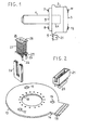
- the printing head is basically constituted by three separated elements: a mechanical assembly 1 which supports and guides the needles, an electromagnet assembly 2 and an element 3 which retains the electromagnetic armatures and adjusts their position.
- the needle support and guiding assembly 1 may be constituted in conventional form as described in the already cited US patent 4,260,270 or in the US Patent N. 4,004,673.
- Needle support and guiding assembly 1 is fixed to the molded electromagnet assembly 2 by means of a plurality of screw (in fig. 1 the heads 7, 8 of two of these screw are visible).
- Such screw clamp a circular flange, integral to assembly 1, against electromagnetic assembly 2.
- Electromagnetic assembly 2 is a unitary element approximately shaped as a circular ring with rectangular section.
- the several electromagnets corresponding to the several needles are radially and uniformly arranged along this ring.
- electromagnetic assembly 2 will be described more in detail together with the description of a process for manufacturing such assembly.
- a tongue 5 extends from electromagnet assembly 2. Such tongue is part of a printed circuit whose shape and function will be better seen afterwards.
- a connecting socket 21 is soldered on it. Each pair of pins of socket 21 is connected to the two terminals of each electromagnet winding.
- a retaining and adjusting element 3 is further coupled to electromagnet assembly 2 by means of the same screws used for coupling of the needle guide assembly 1.
- Element 3 has the function to support and to position the armatures in the plane of the related magnetic circuit; besides, it has the function to adjust the air gap of the electromagnetic structures and to perform a cushioning action when an armature moves from the attraction state to the release state.
- Fig. 2 shows in exploded perspective view the elements forming the electromagnet assembly 2.
- Assembly 2 comprises a ring-shaped printed circuit board 13 provided with an appendix 14 (corresponding to tongue 5 of fig. 1) and three openings 15, 16, 17 of suitable diameter radially arranged and intended for insertion of three screws (like 7 and 9 of fig. 1) clamping needle guide assembly 1 and retaining element 3 to electromagnet assembly 2.
- the printed circuit board 13 has a plurality of hole pairs (in fig. 2 nine pairs are shown, a pair of which is identified by reference numeral 18). These hole pairs are radially arranged near to the inner edge of the ring and intended to receive the connection pins of electric components.
- a corresponding plurality of hole pairs is made on appendix 14, the holes of each pair being arranged according to parallel lines (in fig. 2 only a pair is identified by reference numeral 19).
- the printed circuit board supports on the side not visible in fig. 2 a plurality of soldering pads, one for each of the holes such as those of pairs 18, 19.
- Each pad corresponding to a hole in tongue 14 is electrically connected to a pad corresponding to one of the holes like those of pair 18.
- connection socket 21 Pins 20 of connection socket 21 are inserted into the holes like those of pair 19 and soldered to the corresponding pads.
- Printed circuit board 13 provides connection of the windings of the electromagnet assembly to connection socket 21, and further provides the several individual electromagnets with a temporary mechanical support.
- Each electromagnet of assembly 2 is constituted by a core on which a coil is wound.
- Each core like 26 is constituted by a stack of U - shaped magnetic sheets having two magnetic columns joined by a yoke.
- Each coil like 27 is constituted by a reel 25 made of insulating material and provided with a central opening intended to receive a core column and with two winding containing flanges.
- Two conductive pins 22, 23 are fixed to the lower flange.
- Each of the two winding containing flanges is provided with a reference groove 28, 29 respectively; the function of such grooves will be seen later on.
- the enameled wire forming the coil is wound on the reel.
- wire ends from which the insulation coating has been previously removed, are wrapped around pins 22, 23 and then soldered thereto.
- electromagnet By engaging coil 27 on a column of core 26, an electromagnet is obtained.
- electromagnet can be mounted on printed circuit board 13 as any electric component by inserting pins 22, 23 into holes 18.
- This operation can be easily performed by automated machines.
- Pins 22, 23 are then welded to the conductive pads corresponding to holes 18.
- This anchorage does not obviously suffice to provide the required stiffness to the assembly, but it is suitable for allowing its handling in the manufacturing process as a unitary element.
- the so obtained element is placed into a mold of suitable shape into which a hardening plastic resin is poured or injected.
- the plastic resin is then hardened so as to encase the elements constituting the assembly in a plastic unitary block.
- Figures 3 and 4 show in perspective view the electromagnet assembly according two different orientations so that the electromagnets are seen above and below the printed circuit respectively.
- the encasing plastic body is essentially shaped as a cylinder 30 provided with a central cylindrical opening 41 and with a toroidal neck 31 (below or above, according to whether it is seen in fig. 3 or 4) having a diameter rather greater than the one of cylinder 30.
- the cores of the electromagnets are radially and uniformly arranged into body 30: the columns, on which the windings are inserted, are inward arranged and the columns without windings are arranged outward the cylindrical periphery of body 30. Particularly the outward located columns, from 32 to 40,protude- from the plastic body.
- the mold used for the plastic body molding is provided, at its outward cylindrical periphery, with grooves for housing the core portions which protrude from the plastic body.
- the mold is provided with peripheral guiding grooves which assure the correct transversal and angular positioning into the mold of the assembly constituted by the printed circuit board and by the several electromagnets mounted thereon.
- the protrusion from plastic body 30 of a portion of the external columns provides further a more effective dissipation of the heat which develops into the magnetic circuits by hysterisis and eddy currents when pulsating magnetic fields are induced in such magnetic circuits, that is when the printing head is working.
- Central cylindrical opening 41 has a plurality of axial grooves like 42, 43, 44......... radially arranged in uniform way, each one radially aligned with an electromagnet.
- the mold is provided with a massive central part on the cylindrical periphery of which there are several axial teeth corresponding to grooves 42, 43, 44........
- Such teeth are intended for engagement with grooves 28, 29 present on the reel flanges when the assembly constituted by the printed circuit board and by the electromagnets is inserted into the mold.
- the upper face of cylindrical body 30, as it may be seen in fig. 3, is a bit lowered as to the column height except for three protruding collars 45, 46, 47 arranged round three axial openings 48, 49, 50 of suitable diameter which cross cylindrical body 3 0 and neck 31.
- Axial openings 48, 49, 50 match with holes 15, 16, 17 of printed circuit 13 of fig. 2 and are intended to house the screws (like 7, 8 of fig. 1) which couple the needle guide assembly 1 to electromagnet assembly 2.
- the upper face (in fig. 4) of the electromagnetic assembly shows, besides axial openings 48, 49, 50, a plurality of tapered cavities 51, whil,59 radially arranged and penetrating into the plastic down to the depth of the printed circuit.
- Fig. 5 shows in flow diagram such process.
- the initial raw materials are:
- the magnetic iron sheet is first blanked in the desired shape.
- the magnetic sheets are then deburred, washed, annealed and stored into a stick loader all with equal orientation.
- the enameled wire and the reels feed an automatic coil winder 71 which provides for the wire winding on the reel so as to obtain the desired turn number, for the welding of the wire terminals to the reel pins (like 22, 23 of fig. 2) and for the oriented storing of the coils so obtained into stick loaders.
- the copper clad substrate for printed circuits is subjected to the known operations of blanking, photoengraving and washing and the printed circuit boards so obtained are stored into loaders (block 72 of fig. 5).
- the magnetic sheets are drawn in stacks from the stick loaders by an automatic machine provided with a drawing box.
- the automatic machine receives from another path, one by one, the already prepared coils and inserts a core column into a coil (block 73).
- the so formed electromagnets feed an automatic machine able to insert
- Such machine receives from a path 74 the printed circuit boards and inserts thereon the desired number of electromagnets (block 75).
- the same machine receives from a path 76 the connectors (like 21 of fig. 2) and, in a second station, provides for the connector insertion on printed circuit board (block 77).
- the printed circuit artworks feed a wave soldering station'where the electromagnets and the connector, held in position by a suitable fixture, are soldered to the printed circuit board (block 78). Afterwards the sets so formed cross a washing and subsequent drying station (block 79) and enter in a control station 80 where soldering operation is monitored through automatic conductivity tests for connection quality and through automatic insulation tests for detection of possible shorts.
- plastic material may be used:
- the molding machine provides for the automatic insertions of the sets into the mold and for their encasing (block 81).
- the encased sets cross a shagging station (block 82) where possible overpresses are removed and a curing station (block 83) where the polymerization or the cooling of the plastic material is completed.
- Test operation may then be performed which may be automatia' as regards the measures of insulation and conductivity and visual as regards the inspection of the encased assembly for completeness of the encasing and the absence of blisters and cracks.
- This operation is followed by washing in order to eliminate the powders resulting from the lapping operation (block 86).
- the electromagnet assembly of the present invention may be obtained through a completely automated productive process, except for a few operations of visual inspection, and therefore it is particularly unexpensive.
Landscapes
- Impact Printers (AREA)
- Printers Or Recording Devices Using Electromagnetic And Radiation Means (AREA)
- Electronic Switches (AREA)
- Particle Formation And Scattering Control In Inkjet Printers (AREA)
Priority Applications (1)
| Application Number | Priority Date | Filing Date | Title |
|---|---|---|---|
| AT82101084T ATE19755T1 (de) | 1981-02-25 | 1982-02-13 | Elektromagnetenanordnung fuer mosaik-druckwerke und verfahren zu deren herstellung. |
Applications Claiming Priority (2)
| Application Number | Priority Date | Filing Date | Title |
|---|---|---|---|
| IT19958/81A IT1135613B (it) | 1981-02-25 | 1981-02-25 | Gruppo elettromagnetico per testina stampante a mosaico e relativo metodo di produzione |
| IT1995881 | 1981-02-25 |
Publications (3)
| Publication Number | Publication Date |
|---|---|
| EP0058901A2 true EP0058901A2 (fr) | 1982-09-01 |
| EP0058901A3 EP0058901A3 (en) | 1983-07-20 |
| EP0058901B1 EP0058901B1 (fr) | 1986-05-14 |
Family
ID=11162643
Family Applications (1)
| Application Number | Title | Priority Date | Filing Date |
|---|---|---|---|
| EP82101084A Expired EP0058901B1 (fr) | 1981-02-25 | 1982-02-13 | Ensemble d'électro-aimants pour une tête d'impression en mosaique et son procédé de fabrication |
Country Status (8)
| Country | Link |
|---|---|
| US (1) | US4433927A (fr) |
| EP (1) | EP0058901B1 (fr) |
| JP (1) | JPS57163579A (fr) |
| AT (1) | ATE19755T1 (fr) |
| AU (1) | AU548826B2 (fr) |
| CA (1) | CA1173173A (fr) |
| DE (1) | DE3271097D1 (fr) |
| IT (1) | IT1135613B (fr) |
Cited By (2)
| Publication number | Priority date | Publication date | Assignee | Title |
|---|---|---|---|---|
| WO1984003253A1 (fr) * | 1983-02-25 | 1984-08-30 | Ncr Co | Assemblage de bobine de fil pour une tete imprimante matricielle et son procede de fabrication |
| EP0373427A2 (fr) * | 1988-12-16 | 1990-06-20 | International Business Machines Corporation | Mécanisme de commande avec électro-aimant pour imprimante par percussion et méthode de fabrication |
Families Citing this family (36)
| Publication number | Priority date | Publication date | Assignee | Title |
|---|---|---|---|---|
| US4513496A (en) * | 1983-01-17 | 1985-04-30 | Centronics Data Computer Corp. | Method of making a print pin actuator |
| US4527469A (en) * | 1983-04-15 | 1985-07-09 | Dataproducts Corporation | Dot matrix print actuator |
| JPS6079965A (ja) * | 1983-10-11 | 1985-05-07 | Hitachi Ltd | 印字ヘツド |
| JPS6112353A (ja) * | 1984-06-29 | 1986-01-20 | Nec Home Electronics Ltd | プリンタヘツドバンク |
| JPS621551A (ja) * | 1985-06-28 | 1987-01-07 | Toshiba Corp | 印字ヘツド装置 |
| JPS62148271A (ja) * | 1985-12-24 | 1987-07-02 | Toshiba Corp | ワイヤドツトプリンタヘツドおよびその製作方法 |
| US4886381A (en) * | 1988-05-06 | 1989-12-12 | D. H. Technology, Inc. | Dot matrix print head assembly |
| JPH02196673A (ja) * | 1988-10-28 | 1990-08-03 | Oki Electric Ind Co Ltd | ワイヤドット印字ヘッドの駆動装置 |
| JPH0273334U (fr) * | 1988-11-28 | 1990-06-05 | ||
| US5102245A (en) * | 1989-08-26 | 1992-04-07 | Citizen Watch Co., Ltd. | Print head |
| JPH04135866A (ja) * | 1990-09-28 | 1992-05-11 | Tokyo Electric Co Ltd | ドットプリンタヘッド |
| JPH04175171A (ja) * | 1990-11-09 | 1992-06-23 | Tokyo Electric Co Ltd | ドットプリンタヘッド |
| US7426780B2 (en) * | 2004-11-10 | 2008-09-23 | Enpirion, Inc. | Method of manufacturing a power module |
| US7462317B2 (en) * | 2004-11-10 | 2008-12-09 | Enpirion, Inc. | Method of manufacturing an encapsulated package for a magnetic device |
| US7688172B2 (en) * | 2005-10-05 | 2010-03-30 | Enpirion, Inc. | Magnetic device having a conductive clip |
| US8701272B2 (en) | 2005-10-05 | 2014-04-22 | Enpirion, Inc. | Method of forming a power module with a magnetic device having a conductive clip |
| US8139362B2 (en) * | 2005-10-05 | 2012-03-20 | Enpirion, Inc. | Power module with a magnetic device having a conductive clip |
| US8631560B2 (en) * | 2005-10-05 | 2014-01-21 | Enpirion, Inc. | Method of forming a magnetic device having a conductive clip |
| US7952459B2 (en) | 2007-09-10 | 2011-05-31 | Enpirion, Inc. | Micromagnetic device and method of forming the same |
| US8018315B2 (en) * | 2007-09-10 | 2011-09-13 | Enpirion, Inc. | Power converter employing a micromagnetic device |
| US7920042B2 (en) * | 2007-09-10 | 2011-04-05 | Enpirion, Inc. | Micromagnetic device and method of forming the same |
| US8133529B2 (en) * | 2007-09-10 | 2012-03-13 | Enpirion, Inc. | Method of forming a micromagnetic device |
| US7955868B2 (en) * | 2007-09-10 | 2011-06-07 | Enpirion, Inc. | Method of forming a micromagnetic device |
| US8692532B2 (en) | 2008-04-16 | 2014-04-08 | Enpirion, Inc. | Power converter with controller operable in selected modes of operation |
| US8541991B2 (en) | 2008-04-16 | 2013-09-24 | Enpirion, Inc. | Power converter with controller operable in selected modes of operation |
| US9246390B2 (en) * | 2008-04-16 | 2016-01-26 | Enpirion, Inc. | Power converter with controller operable in selected modes of operation |
| US8686698B2 (en) * | 2008-04-16 | 2014-04-01 | Enpirion, Inc. | Power converter with controller operable in selected modes of operation |
| US8153473B2 (en) * | 2008-10-02 | 2012-04-10 | Empirion, Inc. | Module having a stacked passive element and method of forming the same |
| US8266793B2 (en) * | 2008-10-02 | 2012-09-18 | Enpirion, Inc. | Module having a stacked magnetic device and semiconductor device and method of forming the same |
| US8339802B2 (en) * | 2008-10-02 | 2012-12-25 | Enpirion, Inc. | Module having a stacked magnetic device and semiconductor device and method of forming the same |
| US9054086B2 (en) * | 2008-10-02 | 2015-06-09 | Enpirion, Inc. | Module having a stacked passive element and method of forming the same |
| US8698463B2 (en) * | 2008-12-29 | 2014-04-15 | Enpirion, Inc. | Power converter with a dynamically configurable controller based on a power conversion mode |
| US9548714B2 (en) | 2008-12-29 | 2017-01-17 | Altera Corporation | Power converter with a dynamically configurable controller and output filter |
| US8867295B2 (en) | 2010-12-17 | 2014-10-21 | Enpirion, Inc. | Power converter for a memory module |
| CN102744974A (zh) * | 2011-04-19 | 2012-10-24 | 多美科信息科技(深圳)有限公司 | 针式打印头 |
| US9509217B2 (en) | 2015-04-20 | 2016-11-29 | Altera Corporation | Asymmetric power flow controller for a power converter and method of operating the same |
Citations (6)
| Publication number | Priority date | Publication date | Assignee | Title |
|---|---|---|---|---|
| FR2136517A5 (fr) * | 1971-04-22 | 1972-12-22 | Anker Werke Ag | |
| US3737995A (en) * | 1970-11-19 | 1973-06-12 | Siemens Ag | Method for the production of plastic |
| US3929214A (en) * | 1974-09-18 | 1975-12-30 | D & D Ass | Wire matrix ballistic impact print head |
| US4049107A (en) * | 1974-10-08 | 1977-09-20 | Societe D'applications Generales D'electricite Et De Mecanique Sagem | Printing devices or heads for printers or the like and a process for making such a printing head |
| WO1981000008A1 (fr) * | 1979-06-25 | 1981-01-08 | Gen Electric | Machine a imprimer et son procede de fabrication |
| US4244658A (en) * | 1978-02-01 | 1981-01-13 | Kabushiki Kaisha Suwa Seikosha | Dot printer head |
Family Cites Families (4)
| Publication number | Priority date | Publication date | Assignee | Title |
|---|---|---|---|---|
| JPS5488412A (en) * | 1977-12-24 | 1979-07-13 | Nippon Telegraph & Telephone | Impact dot printing head |
| JPS5488413A (en) * | 1977-12-24 | 1979-07-13 | Nippon Telegraph & Telephone | High speed impact dot printing head |
| JPS54104920A (en) * | 1978-02-01 | 1979-08-17 | Suwa Seikosha Kk | Dot printer head |
| JPS55148177A (en) * | 1979-05-08 | 1980-11-18 | Nec Corp | Printing head for matrix printer |
-
1981
- 1981-02-25 IT IT19958/81A patent/IT1135613B/it active
-
1982
- 1982-02-13 EP EP82101084A patent/EP0058901B1/fr not_active Expired
- 1982-02-13 DE DE8282101084T patent/DE3271097D1/de not_active Expired
- 1982-02-13 AT AT82101084T patent/ATE19755T1/de not_active IP Right Cessation
- 1982-02-19 US US06/350,539 patent/US4433927A/en not_active Expired - Lifetime
- 1982-02-19 AU AU80618/82A patent/AU548826B2/en not_active Ceased
- 1982-02-24 CA CA000397005A patent/CA1173173A/fr not_active Expired
- 1982-02-25 JP JP57029752A patent/JPS57163579A/ja active Granted
Patent Citations (6)
| Publication number | Priority date | Publication date | Assignee | Title |
|---|---|---|---|---|
| US3737995A (en) * | 1970-11-19 | 1973-06-12 | Siemens Ag | Method for the production of plastic |
| FR2136517A5 (fr) * | 1971-04-22 | 1972-12-22 | Anker Werke Ag | |
| US3929214A (en) * | 1974-09-18 | 1975-12-30 | D & D Ass | Wire matrix ballistic impact print head |
| US4049107A (en) * | 1974-10-08 | 1977-09-20 | Societe D'applications Generales D'electricite Et De Mecanique Sagem | Printing devices or heads for printers or the like and a process for making such a printing head |
| US4244658A (en) * | 1978-02-01 | 1981-01-13 | Kabushiki Kaisha Suwa Seikosha | Dot printer head |
| WO1981000008A1 (fr) * | 1979-06-25 | 1981-01-08 | Gen Electric | Machine a imprimer et son procede de fabrication |
Cited By (3)
| Publication number | Priority date | Publication date | Assignee | Title |
|---|---|---|---|---|
| WO1984003253A1 (fr) * | 1983-02-25 | 1984-08-30 | Ncr Co | Assemblage de bobine de fil pour une tete imprimante matricielle et son procede de fabrication |
| EP0373427A2 (fr) * | 1988-12-16 | 1990-06-20 | International Business Machines Corporation | Mécanisme de commande avec électro-aimant pour imprimante par percussion et méthode de fabrication |
| EP0373427A3 (fr) * | 1988-12-16 | 1990-09-12 | International Business Machines Corporation | Mécanisme de commande avec électro-aimant pour imprimante par percussion et méthode de fabrication |
Also Published As
| Publication number | Publication date |
|---|---|
| CA1173173A (fr) | 1984-08-21 |
| JPH0367028B2 (fr) | 1991-10-21 |
| ATE19755T1 (de) | 1986-05-15 |
| IT1135613B (it) | 1986-08-27 |
| EP0058901A3 (en) | 1983-07-20 |
| AU548826B2 (en) | 1986-01-02 |
| AU8061882A (en) | 1982-09-09 |
| IT8119958A0 (it) | 1981-02-25 |
| DE3271097D1 (en) | 1986-06-19 |
| JPS57163579A (en) | 1982-10-07 |
| US4433927A (en) | 1984-02-28 |
| EP0058901B1 (fr) | 1986-05-14 |
Similar Documents
| Publication | Publication Date | Title |
|---|---|---|
| EP0058901B1 (fr) | Ensemble d'électro-aimants pour une tête d'impression en mosaique et son procédé de fabrication | |
| EP0693757B1 (fr) | Inductance et procédé pour sa fabrication | |
| US6311387B1 (en) | Method of manufacturing inductor | |
| US5409558A (en) | Method of manufacturing a gradient magnetic field coil assembly of an MRI apparatus | |
| US6859994B2 (en) | Method for manufacturing an inductor | |
| US5588202A (en) | Method for manufacturing an overmolded sensor | |
| US6815851B2 (en) | Motor, terminal assembly for the motor, and electrical apparatus having the motor | |
| US3838372A (en) | Magnetic pickup assembly | |
| US5023734A (en) | Cylindrical rotary transducer | |
| US4638202A (en) | Commutator and method of making same | |
| US20020008508A1 (en) | High torque electromagnetic devices | |
| US20020057029A1 (en) | Coil holder | |
| JPS6152620B2 (fr) | ||
| WO2000010021A1 (fr) | Procede et accessoire pour evaluer la qualite d'une carcasse de stator lors de sa production | |
| JPS6052565B2 (ja) | コイルモ−ルド体の製造方法 | |
| JPS5886851A (ja) | 平面対向型モ−タの電機子コイル | |
| JPH04282087A (ja) | ソレノイドバルブ | |
| JPH04185252A (ja) | 樹脂モールドモータの固定子 | |
| US4117427A (en) | Standardized component for cross-point matrices | |
| JP2501489Y2 (ja) | アンテナコイル装置の取付け構造 | |
| JPS6026504Y2 (ja) | 扁平形ブラシレスモ−タ | |
| JPH0864452A (ja) | コイル部品の製造方法 | |
| GB2144585A (en) | A transformer bobbin | |
| JPH06251943A (ja) | 電磁機器 | |
| JPH0266903A (ja) | 小形コイル及びその製造方法 |
Legal Events
| Date | Code | Title | Description |
|---|---|---|---|
| PUAI | Public reference made under article 153(3) epc to a published international application that has entered the european phase |
Free format text: ORIGINAL CODE: 0009012 |
|
| AK | Designated contracting states |
Designated state(s): AT BE CH DE FR GB LI NL SE |
|
| PUAL | Search report despatched |
Free format text: ORIGINAL CODE: 0009013 |
|
| AK | Designated contracting states |
Designated state(s): AT BE CH DE FR GB LI NL SE |
|
| 17P | Request for examination filed |
Effective date: 19830718 |
|
| GRAA | (expected) grant |
Free format text: ORIGINAL CODE: 0009210 |
|
| AK | Designated contracting states |
Kind code of ref document: B1 Designated state(s): AT BE CH DE FR GB LI NL SE |
|
| PG25 | Lapsed in a contracting state [announced via postgrant information from national office to epo] |
Ref country code: BE Effective date: 19860514 Ref country code: AT Effective date: 19860514 |
|
| REF | Corresponds to: |
Ref document number: 19755 Country of ref document: AT Date of ref document: 19860515 Kind code of ref document: T |
|
| REF | Corresponds to: |
Ref document number: 3271097 Country of ref document: DE Date of ref document: 19860619 |
|
| ET | Fr: translation filed | ||
| PLBE | No opposition filed within time limit |
Free format text: ORIGINAL CODE: 0009261 |
|
| STAA | Information on the status of an ep patent application or granted ep patent |
Free format text: STATUS: NO OPPOSITION FILED WITHIN TIME LIMIT |
|
| 26N | No opposition filed | ||
| PGFP | Annual fee paid to national office [announced via postgrant information from national office to epo] |
Ref country code: FR Payment date: 19920226 Year of fee payment: 11 |
|
| PGFP | Annual fee paid to national office [announced via postgrant information from national office to epo] |
Ref country code: CH Payment date: 19920530 Year of fee payment: 11 |
|
| PGFP | Annual fee paid to national office [announced via postgrant information from national office to epo] |
Ref country code: DE Payment date: 19930219 Year of fee payment: 12 |
|
| PG25 | Lapsed in a contracting state [announced via postgrant information from national office to epo] |
Ref country code: LI Effective date: 19930228 Ref country code: CH Effective date: 19930228 |
|
| PGFP | Annual fee paid to national office [announced via postgrant information from national office to epo] |
Ref country code: NL Payment date: 19930228 Year of fee payment: 12 |
|
| PGFP | Annual fee paid to national office [announced via postgrant information from national office to epo] |
Ref country code: SE Payment date: 19930803 Year of fee payment: 12 |
|
| PG25 | Lapsed in a contracting state [announced via postgrant information from national office to epo] |
Ref country code: FR Effective date: 19931029 |
|
| REG | Reference to a national code |
Ref country code: CH Ref legal event code: PL |
|
| REG | Reference to a national code |
Ref country code: FR Ref legal event code: ST |
|
| PG25 | Lapsed in a contracting state [announced via postgrant information from national office to epo] |
Ref country code: SE Effective date: 19940214 |
|
| PG25 | Lapsed in a contracting state [announced via postgrant information from national office to epo] |
Ref country code: NL Effective date: 19940901 |
|
| NLV4 | Nl: lapsed or anulled due to non-payment of the annual fee | ||
| PG25 | Lapsed in a contracting state [announced via postgrant information from national office to epo] |
Ref country code: DE Effective date: 19941101 |
|
| EUG | Se: european patent has lapsed |
Ref document number: 82101084.0 Effective date: 19940910 |
|
| PGFP | Annual fee paid to national office [announced via postgrant information from national office to epo] |
Ref country code: GB Payment date: 19960205 Year of fee payment: 15 |
|
| PG25 | Lapsed in a contracting state [announced via postgrant information from national office to epo] |
Ref country code: GB Effective date: 19970213 |
|
| GBPC | Gb: european patent ceased through non-payment of renewal fee |
Effective date: 19970213 |