EP0053712B1 - Procédé pour l'amélioration de la conductivité d'un film microélectroniquement conducteur en siliciure de tungstène et dispositif semi-conducteur contenant ce film - Google Patents
Procédé pour l'amélioration de la conductivité d'un film microélectroniquement conducteur en siliciure de tungstène et dispositif semi-conducteur contenant ce film Download PDFInfo
- Publication number
- EP0053712B1 EP0053712B1 EP81109159A EP81109159A EP0053712B1 EP 0053712 B1 EP0053712 B1 EP 0053712B1 EP 81109159 A EP81109159 A EP 81109159A EP 81109159 A EP81109159 A EP 81109159A EP 0053712 B1 EP0053712 B1 EP 0053712B1
- Authority
- EP
- European Patent Office
- Prior art keywords
- layer
- tungsten silicide
- platinum
- deposited
- film
- Prior art date
- Legal status (The legal status is an assumption and is not a legal conclusion. Google has not performed a legal analysis and makes no representation as to the accuracy of the status listed.)
- Expired
Links
- WQJQOUPTWCFRMM-UHFFFAOYSA-N tungsten disilicide Chemical compound [Si]#[W]#[Si] WQJQOUPTWCFRMM-UHFFFAOYSA-N 0.000 title claims description 78
- 229910021342 tungsten silicide Inorganic materials 0.000 title claims description 74
- 238000000034 method Methods 0.000 title claims description 44
- 238000004377 microelectronic Methods 0.000 title claims description 11
- 239000004065 semiconductor Substances 0.000 title claims description 9
- BASFCYQUMIYNBI-UHFFFAOYSA-N platinum Chemical compound [Pt] BASFCYQUMIYNBI-UHFFFAOYSA-N 0.000 claims description 136
- 229910052697 platinum Inorganic materials 0.000 claims description 45
- 238000004544 sputter deposition Methods 0.000 claims description 41
- 239000000758 substrate Substances 0.000 claims description 32
- VYPSYNLAJGMNEJ-UHFFFAOYSA-N Silicium dioxide Chemical compound O=[Si]=O VYPSYNLAJGMNEJ-UHFFFAOYSA-N 0.000 claims description 29
- 238000000137 annealing Methods 0.000 claims description 29
- 229910021420 polycrystalline silicon Inorganic materials 0.000 claims description 25
- 238000000151 deposition Methods 0.000 claims description 23
- 238000010549 co-Evaporation Methods 0.000 claims description 18
- 230000008021 deposition Effects 0.000 claims description 18
- 238000001704 evaporation Methods 0.000 claims description 15
- 230000008020 evaporation Effects 0.000 claims description 15
- 239000000377 silicon dioxide Substances 0.000 claims description 14
- 235000012239 silicon dioxide Nutrition 0.000 claims description 14
- 229910052721 tungsten Inorganic materials 0.000 claims description 13
- 239000012298 atmosphere Substances 0.000 claims description 10
- 239000000203 mixture Substances 0.000 claims description 9
- 229910052710 silicon Inorganic materials 0.000 claims description 9
- WFKWXMTUELFFGS-UHFFFAOYSA-N tungsten Chemical group [W] WFKWXMTUELFFGS-UHFFFAOYSA-N 0.000 claims description 9
- 239000010937 tungsten Substances 0.000 claims description 8
- 230000001590 oxidative effect Effects 0.000 claims description 7
- 239000000843 powder Substances 0.000 claims description 7
- XUIMIQQOPSSXEZ-UHFFFAOYSA-N Silicon Chemical compound [Si] XUIMIQQOPSSXEZ-UHFFFAOYSA-N 0.000 claims description 6
- 238000007731 hot pressing Methods 0.000 claims description 6
- 229910021339 platinum silicide Inorganic materials 0.000 claims description 6
- 239000010703 silicon Substances 0.000 claims description 5
- 238000005477 sputtering target Methods 0.000 claims description 4
- 239000011863 silicon-based powder Substances 0.000 claims description 2
- ZXEYZECDXFPJRJ-UHFFFAOYSA-N $l^{3}-silane;platinum Chemical compound [SiH3].[Pt] ZXEYZECDXFPJRJ-UHFFFAOYSA-N 0.000 claims 1
- 229910008814 WSi2 Inorganic materials 0.000 description 63
- 239000010408 film Substances 0.000 description 47
- 239000010409 thin film Substances 0.000 description 21
- XKRFYHLGVUSROY-UHFFFAOYSA-N Argon Chemical compound [Ar] XKRFYHLGVUSROY-UHFFFAOYSA-N 0.000 description 8
- 230000008901 benefit Effects 0.000 description 8
- 230000008569 process Effects 0.000 description 8
- 238000009792 diffusion process Methods 0.000 description 7
- 239000000463 material Substances 0.000 description 7
- 230000003647 oxidation Effects 0.000 description 6
- 238000007254 oxidation reaction Methods 0.000 description 6
- 230000015572 biosynthetic process Effects 0.000 description 5
- 229910021419 crystalline silicon Inorganic materials 0.000 description 5
- 238000012545 processing Methods 0.000 description 5
- IJGRMHOSHXDMSA-UHFFFAOYSA-N Atomic nitrogen Chemical compound N#N IJGRMHOSHXDMSA-UHFFFAOYSA-N 0.000 description 4
- 229910052786 argon Inorganic materials 0.000 description 4
- 239000004020 conductor Substances 0.000 description 4
- 238000002474 experimental method Methods 0.000 description 4
- 238000004519 manufacturing process Methods 0.000 description 4
- 229910021421 monocrystalline silicon Inorganic materials 0.000 description 4
- 229910021332 silicide Inorganic materials 0.000 description 4
- FVBUAEGBCNSCDD-UHFFFAOYSA-N silicide(4-) Chemical compound [Si-4] FVBUAEGBCNSCDD-UHFFFAOYSA-N 0.000 description 4
- VLJQDHDVZJXNQL-UHFFFAOYSA-N 4-methyl-n-(oxomethylidene)benzenesulfonamide Chemical compound CC1=CC=C(S(=O)(=O)N=C=O)C=C1 VLJQDHDVZJXNQL-UHFFFAOYSA-N 0.000 description 3
- 230000007797 corrosion Effects 0.000 description 3
- 238000005260 corrosion Methods 0.000 description 3
- 239000007789 gas Substances 0.000 description 3
- 239000000126 substance Substances 0.000 description 3
- 239000012300 argon atmosphere Substances 0.000 description 2
- 150000001875 compounds Chemical class 0.000 description 2
- 230000003247 decreasing effect Effects 0.000 description 2
- 230000005669 field effect Effects 0.000 description 2
- 230000006872 improvement Effects 0.000 description 2
- 239000011261 inert gas Substances 0.000 description 2
- 150000002500 ions Chemical class 0.000 description 2
- 229910052757 nitrogen Inorganic materials 0.000 description 2
- 238000002161 passivation Methods 0.000 description 2
- 229910021340 platinum monosilicide Inorganic materials 0.000 description 2
- 230000001737 promoting effect Effects 0.000 description 2
- 238000001552 radio frequency sputter deposition Methods 0.000 description 2
- 239000003870 refractory metal Substances 0.000 description 2
- 238000012360 testing method Methods 0.000 description 2
- -1 tungsten silicide compound Chemical class 0.000 description 2
- UFHFLCQGNIYNRP-UHFFFAOYSA-N Hydrogen Chemical compound [H][H] UFHFLCQGNIYNRP-UHFFFAOYSA-N 0.000 description 1
- 229910006774 Si—W Inorganic materials 0.000 description 1
- 238000004458 analytical method Methods 0.000 description 1
- 244000309464 bull Species 0.000 description 1
- 230000015556 catabolic process Effects 0.000 description 1
- 230000008859 change Effects 0.000 description 1
- 239000013043 chemical agent Substances 0.000 description 1
- 238000006243 chemical reaction Methods 0.000 description 1
- 238000000576 coating method Methods 0.000 description 1
- 239000002131 composite material Substances 0.000 description 1
- 238000002425 crystallisation Methods 0.000 description 1
- 230000008025 crystallization Effects 0.000 description 1
- 230000007423 decrease Effects 0.000 description 1
- 230000007812 deficiency Effects 0.000 description 1
- 238000006731 degradation reaction Methods 0.000 description 1
- 230000001419 dependent effect Effects 0.000 description 1
- 238000011161 development Methods 0.000 description 1
- 239000002019 doping agent Substances 0.000 description 1
- 230000000694 effects Effects 0.000 description 1
- 238000010292 electrical insulation Methods 0.000 description 1
- 238000005516 engineering process Methods 0.000 description 1
- 229910000078 germane Inorganic materials 0.000 description 1
- 239000001257 hydrogen Substances 0.000 description 1
- 229910052739 hydrogen Inorganic materials 0.000 description 1
- 230000007246 mechanism Effects 0.000 description 1
- 238000001465 metallisation Methods 0.000 description 1
- 230000001681 protective effect Effects 0.000 description 1
- 230000009467 reduction Effects 0.000 description 1
- 238000011160 research Methods 0.000 description 1
- 238000012552 review Methods 0.000 description 1
- 238000007788 roughening Methods 0.000 description 1
- 238000011282 treatment Methods 0.000 description 1
- 235000012431 wafers Nutrition 0.000 description 1
Images
Classifications
-
- H—ELECTRICITY
- H01—ELECTRIC ELEMENTS
- H01L—SEMICONDUCTOR DEVICES NOT COVERED BY CLASS H10
- H01L21/00—Processes or apparatus adapted for the manufacture or treatment of semiconductor or solid state devices or of parts thereof
- H01L21/02—Manufacture or treatment of semiconductor devices or of parts thereof
- H01L21/04—Manufacture or treatment of semiconductor devices or of parts thereof the devices having potential barriers, e.g. a PN junction, depletion layer or carrier concentration layer
- H01L21/18—Manufacture or treatment of semiconductor devices or of parts thereof the devices having potential barriers, e.g. a PN junction, depletion layer or carrier concentration layer the devices having semiconductor bodies comprising elements of Group IV of the Periodic Table or AIIIBV compounds with or without impurities, e.g. doping materials
- H01L21/28—Manufacture of electrodes on semiconductor bodies using processes or apparatus not provided for in groups H01L21/20 - H01L21/268
- H01L21/283—Deposition of conductive or insulating materials for electrodes conducting electric current
- H01L21/285—Deposition of conductive or insulating materials for electrodes conducting electric current from a gas or vapour, e.g. condensation
- H01L21/28506—Deposition of conductive or insulating materials for electrodes conducting electric current from a gas or vapour, e.g. condensation of conductive layers
- H01L21/28512—Deposition of conductive or insulating materials for electrodes conducting electric current from a gas or vapour, e.g. condensation of conductive layers on semiconductor bodies comprising elements of Group IV of the Periodic Table
- H01L21/28518—Deposition of conductive or insulating materials for electrodes conducting electric current from a gas or vapour, e.g. condensation of conductive layers on semiconductor bodies comprising elements of Group IV of the Periodic Table the conductive layers comprising silicides
-
- H—ELECTRICITY
- H01—ELECTRIC ELEMENTS
- H01L—SEMICONDUCTOR DEVICES NOT COVERED BY CLASS H10
- H01L29/00—Semiconductor devices specially adapted for rectifying, amplifying, oscillating or switching and having potential barriers; Capacitors or resistors having potential barriers, e.g. a PN-junction depletion layer or carrier concentration layer; Details of semiconductor bodies or of electrodes thereof ; Multistep manufacturing processes therefor
- H01L29/40—Electrodes ; Multistep manufacturing processes therefor
- H01L29/43—Electrodes ; Multistep manufacturing processes therefor characterised by the materials of which they are formed
- H01L29/45—Ohmic electrodes
- H01L29/456—Ohmic electrodes on silicon
-
- H—ELECTRICITY
- H01—ELECTRIC ELEMENTS
- H01L—SEMICONDUCTOR DEVICES NOT COVERED BY CLASS H10
- H01L29/00—Semiconductor devices specially adapted for rectifying, amplifying, oscillating or switching and having potential barriers; Capacitors or resistors having potential barriers, e.g. a PN-junction depletion layer or carrier concentration layer; Details of semiconductor bodies or of electrodes thereof ; Multistep manufacturing processes therefor
- H01L29/40—Electrodes ; Multistep manufacturing processes therefor
- H01L29/43—Electrodes ; Multistep manufacturing processes therefor characterised by the materials of which they are formed
- H01L29/49—Metal-insulator-semiconductor electrodes, e.g. gates of MOSFET
- H01L29/4966—Metal-insulator-semiconductor electrodes, e.g. gates of MOSFET the conductor material next to the insulator being a composite material, e.g. organic material, TiN, MoSi2
- H01L29/4975—Metal-insulator-semiconductor electrodes, e.g. gates of MOSFET the conductor material next to the insulator being a composite material, e.g. organic material, TiN, MoSi2 being a silicide layer, e.g. TiSi2
-
- Y—GENERAL TAGGING OF NEW TECHNOLOGICAL DEVELOPMENTS; GENERAL TAGGING OF CROSS-SECTIONAL TECHNOLOGIES SPANNING OVER SEVERAL SECTIONS OF THE IPC; TECHNICAL SUBJECTS COVERED BY FORMER USPC CROSS-REFERENCE ART COLLECTIONS [XRACs] AND DIGESTS
- Y10—TECHNICAL SUBJECTS COVERED BY FORMER USPC
- Y10S—TECHNICAL SUBJECTS COVERED BY FORMER USPC CROSS-REFERENCE ART COLLECTIONS [XRACs] AND DIGESTS
- Y10S438/00—Semiconductor device manufacturing: process
- Y10S438/934—Sheet resistance, i.e. dopant parameters
Definitions
- the invention relates to a method of improving the conductivity of a microelectronic conductive tungsten silicide film and to semiconductor devices containing said highly conductive WSi 2 layers for contacts and conductors and for FET (field-effect transistor) gates.
- Tungsten silicide (WSi 2 ) has been known to have metallic conductivity and relatively low electrical resistivity. Typical ranges are approximately 33 ,uQ-cm in bulk form, as described in the CRC Handbook of Chemistry and Physics, (1980). However, only recently has it been recognized that low resistivity is achieved in thin films of tungsten silicide. With this development, reported by Crowder and Zirinsky, IEEE J. Solid-State Circuits, SC-14-291 (1979); Mohammadi and Saraswat J-Electrochem. Soc., 127, 450 (1980), it has become apparent that tungsten silicide thin films potentially have microelectronic applications.
- the method employed in the prior art Crowder and Zirinsky proposal for depositing thin films used the technique of co-evaporation followed by annealing in an oxygen-free atmosphere temperatures ranging 800°C ⁇ 1000°C.
- co-evaporation the thin film is deposited onto a substrate while placed in a high-vacuum chamber.
- Two evaporation sources, one containing tungsten and the other silicon, are heated to temperatures such that evaporation of atoms from each source occurs.
- the atoms travel through the high vacuum of the evaporation chamber until they reach and adhere to a relatively colder surface. Some of the evaporated atoms therefore, impinge and condense onto substrates placed within the chamber.
- a WSi 2 layer may be employed as a highly conductive layer for FET gates.
- the substrate is likely to possess chemical vapor deposited polycrystalline silicon as its top-most layer onto which the WSi 2 is co-evaporated.
- the resulting structure is a two-layer element comprising co-evaporated WSi 2 on top of polycrystalline silicon.
- the structure so formed is capable of withstanding high temperature processing, is self-passivating, and generally can be 10 times lower in sheet resistance than the heavily doped polycrystalline silicon layer of the same total thickness.
- the process conditions are difficult to maintain because it is necessary to independently monitor and control in tandem the deposition rates from two evaporation sources operating simultaneously.
- the control of rates of deposition is crucial to prevent either source from pulling the film composition away from the stoichiometry.
- deviation from stoichiometry occurs, the properties of the film suffer. Electrical conductivity is decreased and the ability of the film to passivate itself under oxidizing annealing conditions can be inhibited.
- the process of sputtering is distinct from co-evaporation in that, since the atoms are ejected from the target by the impact of inert gas ions rather than by evaporation, deposition rate control is achieved by controlling the voltage and electrical power applied to the target, rather than by controlling its temperature. Furthermore, it is possible to sputter deposit a thin film of tungsten silicide from a source made up of tungsten silicide compound so that the control of only one source rather than two is required. This reduction in process complication is a material advantage in semiconductor manufacture. The deposition of tungsten silicide thin film by sputtering is thereby generally simpler than deposition by co-evaporation.
- sputter deposited WSi 2 has distinct advantages over co-evaporated WSi 2 .
- WSi 2 has several desirable properties such as metallic conductivity and oxidation resistance in air at 900°C, however, it refers specifically to avoiding its formation at contact areas.
- the formation in contact areas was reported as having effects ranging from no change in contact resistivity to an electrical "open condition".
- Patents such as U.S. Patent 4 141 022 also disclose a refractory metal contact system used for an IGFET wherein PtSi forms an underlayer and a sputter deposited film of TiW forms the upper layer of the contact system.
- Other patent literature that has been considered but deemed to be not specifically germane include U.S. Patents: 3 777 364; 3 806 361 3 906 540; and 3 950 233.
- tungsten silicide Since the resistivity of the heavily doped polycrystalline silicon is about 600 ,uQcm, a sizable conductivity advantage is achieved by using tungsten silicide.
- a protective thin film layer of silicon dioxide can be produced by thermal oxidation of tungsten silicide films deposited onto polycrystalline silicon or single crystalline silicon substrates (see: Zirinsky, et al., Appl. Phys. Lett. 33, 76 (1978)).
- Such a thermally grown overlayer of silicon dioxide provides both good corrosion resistance and electrical insulation.
- the mechanism by which the silicon dioxide layer can be thermally grown without harming the tungsten silicide layer is believed to be by the diffusion of silicon atoms from the substrate through the thin film layer to the upper surface of the WSi 2 layer. Oxidation of the silicon atoms to form silicon dioxide then occurs at the upper surface.
- Another object of this invention is to define a conductive layer for microelectronic applications which possesses the above properties and which accepts thermal oxidation when deposited onto polycrystalline or single crystal silicon.
- Another object of this invention is to define the process utilizing the known advantage of sputtering WSi 2 and obtaining electrical conductivity values comparable to those evident in annealed co-evaporated WSi 2 while lowering the annealing temperature to a level similar to those employed in co-evaporation techniques.
- Yet another object of this invention is to define a thin platinum interface layer used between polycrystalline or single crystal silicon and sputtered or co-evaporated WSi2 to achieve high conductivity in the sputtered WSi 2 layer.
- Still another object of this invention is to define a thin platinum layer used on top of sputtered or co-evaporated WSi 2 to achieve high conductivity in the WSi 2 layer.
- a still further object of this invention is to define an improved FET gate utilizing a highly conductive layer of Pt incorporated with sputtered or co-evaporated WSi 2 to improve the conductivity of the gate.
- the objects of the invention are achieved by a method for improving the conductivity of a tungsten silicide film which is characterized in that adjacent to the tungsten silicide layer a layer of platinum is arranged, and that the structure is annealed to diffuse platinum atoms throughout the tungsten silcide film.
- the present invention employs a layer of Pt in conjunction with sputter deposited or co-evaporated WSi 2 to enhance the conductivity increase of the WSi 2 layer occurring during annealing.
- the Pt is deposited as a thin layer directly atop or beneath the WSi 2 layer, or may be incorporated within the WSi 2 layer.
- the platinum interface layer can be used with either sputtered or co-evaporated WSi 2 films, the preferred technique is to use sputtering techniques. By using the platinum interface layer, the resistivity of the sputtered or co-evaporated tungsten silicide is lowered beyond those values which typically have been achieved.
- the method in accordance with the present invention involves the deposition of a thin-film layer of platinum either directly below or directly above the tungsten silicide layer followed by diffusion of platinum into the tungsten silicide.
- the diffusion of platinum into the tungsten silicide occurs during subsequent high temperature annealing included in the fabrication of the microelectronic circuit.
- the platinum layer thickness is chosen to be approximately 10% of the thickness of the tungsten silicide layer.
- the resulting annealed tungsten silicide film having platinum atoms diffused into it has demonstrated lower resistivity values than in comparably deposited annealed films in which the platinum layer has been omitted.
- the film can still be oxidized to produce a silicon dioxide passivation layer.
- This technique is known and has been described for use with tungsten silicide layers per se. Utilizing this method, either co-evaporated or sputtered tungsten silicide films can be used. However, the most significant decreases in resisitivity have been achieved with sputtered films. This is contrasted with the appreciably high resistivities that has been reported with sputtered films alone when compared to co-evaporated films.
- a novel structure for contacts and for conductors of semiconductor devices and for gates of FET semiconductor devices having a conductivity promoting layer of platinum and a tungsten silicide layer deposited onto a suitable substrate.
- the substrate will contain a top-most layer of polycrystalline silicon, however, single crystal silicon or other suitable materials comprising or deposited onto the substrate may be present in place of the polycrystalline silicon layer.
- the layering can be reversed with the platinum serving either as an underlayer or an overlayer to the WSi 2 . Also, alternate multiple layers of platinum and tungsten silicide can be utilized.
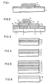
- a first typical structure utilizing tungsten silicide layers for microelectronic applications is shown.
- a polycrystalline silicon layer 3 and a tungsten silicide layer 4 are deposited and patterned on a substrate 1.
- a cover layer 5 is typically deposited or thermally grown silicon dioxide and covers the layers 3 and 4.
- Fig. 2 shows an application wherein the polycrystalline silicon and tungsten silicide layers act as a gate electrode of a field-effect transistor (FET).
- the substrate 1 includes a thin silicon dioxide layer 2 onto which the polycrystalline silicon layer 3 and the tungsten silicide layer 4 are then deposited.
- an insulating layer of silicon dioxide 5 covers the layers 3 and 4.
- the gate structure also includes a layer 6 of polycrystalline silicon and a second layer 7 of tungsten silicide. These two layers are electrically insulated from the lower layers 3 and 4 by the dielectric silicon dioxide layer 5. The layers are passivated by a second dielectric layer 8.
- a first preferred embodiment of the present invention is shown as a cutaway schematic cross-section.
- a platinum layer 9 having a thickness in the range of 10-40 nm is deposited onto a substrate 1 composed of or overlaid with a single crystalline or polycrystalline silicon layer 3.
- the platinum layer may be deposited by conventional means of evaporation or sputtering.
- the tungsten siiicide layer 4 is deposited by co-evaporation or by sputtering to a thickness of typically 100-500 nm.
- the resulting structure is then ready for annealing.
- the platinum layer 9 is approximately 10% of the thickness of the tungsten silicide layer 4..
- Fig. 3 describes an embodiment wherein platinum is the underlayer.
- Fig. 4 shows the converse situation wherein the tungsten silicide and platinum depositions have been reversed.
- the same substrate layers 1 and 3 comprise a single crystalline or polycrystalline silicon layer 3 comprising or deposited onto a suitable substrate 1 the same as in Fig. 3 embodiment.
- the tungsten silicide layer 4 is deposited directly on the substrate layer 3 followed by an overlayer of platinum 9.
- the relationship of thickness, namely the platinum layer being approximately 10% the thickness of the tungsten silicide layer, is true in the Fig. 4 embodiment.
- a third preferred embodiment of this invention is shown where thicker layers of tungsten silicide are desired.
- the identical substrate as in Figs. 3 and 4 embodiments are utilized with a substrate layer 3 comprising single crystalline or polycrystalline silicon.
- alternate layers of tungsten silicide 4 and platinum 9 are deposited.
- the Fig. 5 shows three such composite layers. The use of multiple layers permits more rapid diffusion of platinum atoms throughout the tungsten silicide than would occur with a single platinum underlayer or overlayer. This more rapid diffusion of platinum permits shorter annealing times than would otherwise be required.
- Alternating layer depositions are easily achieved in several commercially available sputtering systems having the capacity for more than one sputtering target or in evaporation systems with multiple sources. While Fig. 5 shows three alternate layers that is, a total of 6 layers of platinum and tungsten silicide, it is apparent that the number is only illustrative. More or fewer layers can be utilized. Also, while Fig. 5 shows a platinum underlayer system, it is apparent that consistent with the embodiment of Fig. 4 the layering may be reversed with the tungsten silicide deposited directly on top of the substrate layer 3 followed by platinum layer 9, second layer of tungsten silicide, a second layer of platinum and so on. That is, the layered structure may begin with either a platinum layer or a tungsten silicide layer, and may end with either layer.
- annealing occurs for a sufficient length of time at a temperature of 800°C or higher.
- the resulting film structure is that depicted in Fig. 6 wherein a layer 10 over the substrate layer 1 exists having tunsten silicide containing platinum. As shown in Fig. 6, a discrete platinum layer no longer exists following the step of annealing.
- the Fig. 6 structure can be verified by Auger sputter profiling analysis of properly annealed films prepared utilizing the embodiments of Figs. 3, 4 or 5.
- the resulting layer 10 shown in Fig. 6 can then be patterned and oxidized as desired, for example that shown in Figs.
- the passivation layer such as layer 5 of Figs. 1 and 2 is to be deposited, rather than being thermally grown silicon dioxide, the constraint that the uppermost layer of the substrate prior to platinum and tungsten silicide deposition be single crystalline or polycrystalline silicon is no longer mandatory.
- the substrates for this series of experiments were lightly doped-n-type (100)-oriented single crystal silicon wafers onto which 600 nm of polycrystalline silicon had been deposited by low pressure chemical vapor depositon. Onto these substrates, a 20 nm layer of Pt and a 400-500 nm layer of WSi 2 were deposited by sputtering. On control samples, the Pt layer was omitted.
- the sputter deposition system used was a Materials Research Corporation Model 822 "sputtersphere" operated in a rf diode configuration.
- the sputtering system accomodates multiple targets (up to a maximum of four) which can be sequentially rotated into position for sputtering.
- Round planar targets of 8-inch (20.32 cm) diameter were used, one target composed of Pt and the other made of hot-pressed WSi2 powder.
- Target powers of 400-500 watts were used with a sputtering pressure of 1.3 Pa of argon gas.
- the sputtering chamber was evacuated to a pressure less than 1.3x10- 4 Pa prior to admitting the argon sputtering atmosphere.
- Typical deposition rates under these operating conditions were 20 nm/min for Pt and 12 nm/min for WSi 2 . Comparisons were then made of the sheet resistance values of co-evaporated WSi 2 sputtered WSi 2 and sputtered Pt/WSi 2 structures after annealing for one hour in a non-oxidizing atmosphere at various temperatures.
- the sputtered Pt/WSi 2 structure has a higher conductivity value (lower sheet resistance) than sputtered WSi 2 alone.
- the values which are obtained using Pt/WSi 2 are comparable to those which have been achieved utilizing co-evaporated WSi 2 .
- a degree of surface roughening was noted upon annealing of the Pt/WSi 2 structure at temperatures in the range of 1000 0- 11 100°C. This surface texturing may be decreased by utilizing a thinner layer of Pt.
- a power splitting feature on this system allowed a tungsten target and a silicon target to be simultaneously powered at selectable levels to achieve the desired stoichiometry in the co-sputtered WSi 2 film.
- Annealing was done for 1 hour in a non-oxidizing atmosphere of argon or nitrogen or a "forming gas" (nitrogen/hydrogen mixture).
- the results were normalized and compared with the data obtained in Experiment in Table I which utilize a Pt underlayer.
- Table III summarizes the data.
- the WSi 2 films used in this experiment were in most cases thinner than the 400-500 nm film thickness employed in the testing done pursuant to Example I.
- Table III presents sheet resistance values obtained pursuant to this example that have been normalized to values that would be applicable to films having a comparable thickness, that is 400 nm.
- co-evaporation refers to simultaneous evaporation of W and Si from separate sources at evaporation rates adjusted to yield a deposited film of the desired stoichiometry.
- Co-sputtering means simultaneous sputter deposition of W and Si from separate W and Si sputtering targets. Each target is powered to an appropriate level such that the sputter-deposition rates produces a deposited film having the desired stoichiometry.
- Co-sputtering is compared with the sputtering techniques utilized in Example II where previous films were produced by sputter deposition from a single target comprising a hot-pressed powder of WSi 2 compound.
- the present invention offers material improvements in processing or allowing the utilization of less complicated sputtering techniques, yet, utilizing annealing temperatures which are comparable to those used in conjunction with co-evaporation of WSi 2 .
- a sputtering target containing Pt and WSi 2 could be employed.
- a target could be prepared by one of the following methods: (a) hot-pressing a mixture of Pt and WSi 2 powders; (b) hot-pressing a mixture of PtSi and WSi 2 powders; or (c) reactively hot-pressing a mixture of Pt, W and Si powders.
- strips, segments or a wire mesh of Pt could be mounted across the face of a WSi 2 target and the samples rotated to obtain better uniformity. This techniques is disclosed in IBM Tech. Disclo. Bull. 20, 1597 (1977) and IEEE Trans. Magnet. MAG-14, 941 (1978). Adjustment of the segment proposition or wire size allows tailoring of the Pt to WSi 2 proportion to the desired composition.
- Sputtering from such a target would produce results similar to those presented in the examples, i.e., a deposited film having Pt atoms incorporated throughout the WSi 2 layer.
- Annealing would still be required to attain high conductivity. This is because annealing induces crystallization and grain growth in the WSi 2 which is typically deposited as an amorphous material, whether by sputtering or co-evaporation. Since the Pt atoms would be incorporated in the WSi2 layer in the same manner as observed using Auger techniques, an enhancement of the post-annealing conductivity of the sputtered WSi 2 will occur, commensurate with that presented herein for layered Pt/WSi 2 structure subjected to annealing.
Landscapes
- Engineering & Computer Science (AREA)
- Microelectronics & Electronic Packaging (AREA)
- Power Engineering (AREA)
- General Physics & Mathematics (AREA)
- Computer Hardware Design (AREA)
- Physics & Mathematics (AREA)
- Condensed Matter Physics & Semiconductors (AREA)
- Ceramic Engineering (AREA)
- Chemical & Material Sciences (AREA)
- Composite Materials (AREA)
- Materials Engineering (AREA)
- Manufacturing & Machinery (AREA)
- Electrodes Of Semiconductors (AREA)
- Physical Vapour Deposition (AREA)
- Internal Circuitry In Semiconductor Integrated Circuit Devices (AREA)
Claims (13)
Applications Claiming Priority (2)
| Application Number | Priority Date | Filing Date | Title |
|---|---|---|---|
| US06/214,170 US4322453A (en) | 1980-12-08 | 1980-12-08 | Conductivity WSi2 (tungsten silicide) films by Pt preanneal layering |
| US214170 | 1980-12-08 |
Publications (2)
| Publication Number | Publication Date |
|---|---|
| EP0053712A1 EP0053712A1 (fr) | 1982-06-16 |
| EP0053712B1 true EP0053712B1 (fr) | 1984-09-12 |
Family
ID=22798043
Family Applications (1)
| Application Number | Title | Priority Date | Filing Date |
|---|---|---|---|
| EP81109159A Expired EP0053712B1 (fr) | 1980-12-08 | 1981-10-29 | Procédé pour l'amélioration de la conductivité d'un film microélectroniquement conducteur en siliciure de tungstène et dispositif semi-conducteur contenant ce film |
Country Status (4)
| Country | Link |
|---|---|
| US (1) | US4322453A (fr) |
| EP (1) | EP0053712B1 (fr) |
| JP (1) | JPS5797651A (fr) |
| DE (1) | DE3166074D1 (fr) |
Families Citing this family (28)
| Publication number | Priority date | Publication date | Assignee | Title |
|---|---|---|---|---|
| US4424101A (en) | 1980-11-06 | 1984-01-03 | The Perkin-Elmer Corp. | Method of depositing doped refractory metal silicides using DC magnetron/RF diode mode co-sputtering techniques |
| US4349408A (en) * | 1981-03-26 | 1982-09-14 | Rca Corporation | Method of depositing a refractory metal on a semiconductor substrate |
| US4700215A (en) * | 1981-11-19 | 1987-10-13 | Texas Instruments Incorporated | Polycide electrodes for integrated circuits |
| US4816425A (en) * | 1981-11-19 | 1989-03-28 | Texas Instruments Incorporated | Polycide process for integrated circuits |
| GB2114809B (en) * | 1982-02-04 | 1986-02-05 | Standard Telephones Cables Ltd | Metallic silicide production |
| JPS59110179A (ja) * | 1982-12-16 | 1984-06-26 | Hitachi Ltd | 半導体装置およびその製造法 |
| JPS59154040A (ja) * | 1983-02-22 | 1984-09-03 | Toshiba Corp | 半導体装置の製造方法 |
| US4529619A (en) * | 1984-07-16 | 1985-07-16 | Xerox Corporation | Ohmic contacts for hydrogenated amorphous silicon |
| US4526665A (en) * | 1984-08-20 | 1985-07-02 | Gould Inc. | Method of depositing fully reacted titanium disilicide thin films |
| US4751198A (en) * | 1985-09-11 | 1988-06-14 | Texas Instruments Incorporated | Process for making contacts and interconnections using direct-reacted silicide |
| US4737474A (en) * | 1986-11-17 | 1988-04-12 | Spectrum Cvd, Inc. | Silicide to silicon bonding process |
| GB8629409D0 (en) * | 1986-12-09 | 1987-01-21 | Evans B L | Multilayered structures |
| JPS6489470A (en) * | 1987-09-30 | 1989-04-03 | Mitsubishi Electric Corp | Manufacture of semiconductor device |
| EP0388565B1 (fr) * | 1988-02-11 | 1996-06-05 | STMicroelectronics, Inc. | Chapeau de siliciure de métal réfractaire, pour protéger les structures multicouches de polycide |
| US5130172A (en) * | 1988-10-21 | 1992-07-14 | The Regents Of The University Of California | Low temperature organometallic deposition of metals |
| US4992152A (en) * | 1989-04-20 | 1991-02-12 | Eastman Kodak Company | Reducing hillocking in aluminum layers formed on substrates |
| AT399419B (de) * | 1989-09-21 | 1995-05-26 | Int Rectifier Corp | Verfahren zur einführung von platinatomen in eine siliziumscheibe zur verringerung der minoritätsträger-lebensdauer |
| US4925812A (en) * | 1989-09-21 | 1990-05-15 | International Rectifier Corporation | Platinum diffusion process |
| US5093274A (en) * | 1990-02-02 | 1992-03-03 | Mitsubishi Denki Kabushiki Kaisha | Semiconductor device and method for manufacture thereof |
| JPH05206394A (ja) * | 1992-01-24 | 1993-08-13 | Mitsubishi Electric Corp | 電界効果トランジスタおよびその製造方法 |
| JP2677168B2 (ja) * | 1993-09-17 | 1997-11-17 | 日本電気株式会社 | 半導体装置の製造方法 |
| US5624869A (en) * | 1994-04-13 | 1997-04-29 | International Business Machines Corporation | Method of forming a film for a multilayer Semiconductor device for improving thermal stability of cobalt silicide using platinum or nitrogen |
| US5849629A (en) * | 1995-10-31 | 1998-12-15 | International Business Machines Corporation | Method of forming a low stress polycide conductors on a semiconductor chip |
| US6187617B1 (en) | 1999-07-29 | 2001-02-13 | International Business Machines Corporation | Semiconductor structure having heterogeneous silicide regions and method for forming same |
| US6351578B1 (en) * | 1999-08-06 | 2002-02-26 | Gemfire Corporation | Thermo-optic switch having fast rise-time |
| US6294435B1 (en) | 1999-10-08 | 2001-09-25 | Vanguard International Semiconductor Corporation | Method of reducing word line resistance and contact resistance |
| DE102004039967B4 (de) * | 2004-08-18 | 2006-10-12 | Gkn Driveline International Gmbh | Verfahren zum Rückwärtsfließpressen von Innenprofilen |
| US7749877B2 (en) * | 2006-03-07 | 2010-07-06 | Siliconix Technology C. V. | Process for forming Schottky rectifier with PtNi silicide Schottky barrier |
Citations (1)
| Publication number | Priority date | Publication date | Assignee | Title |
|---|---|---|---|---|
| SU737498A1 (ru) * | 1978-11-10 | 1980-06-02 | Белорусский Ордена Трудового Красного Знамени Политехнический Институт | Состав дл вольфрамосилицировани стальных изделий |
Family Cites Families (8)
| Publication number | Priority date | Publication date | Assignee | Title |
|---|---|---|---|---|
| GB989469A (en) * | 1962-02-15 | 1965-04-22 | Gen Electric | Formation of corrosion resistant silicide coatings on metal compositions |
| DE1521529C3 (de) * | 1965-06-15 | 1974-11-28 | Telefunken Patentverwertungsgesellschaft Mbh, 7900 Ulm | Verfahren zur Herstellung von feinen Strukturen auf einem Substrat |
| US3614547A (en) * | 1970-03-16 | 1971-10-19 | Gen Electric | Tungsten barrier electrical connection |
| CA1004964A (en) * | 1972-05-30 | 1977-02-08 | Union Carbide Corporation | Corrosion resistant coatings and process for making the same |
| GB1583835A (en) * | 1977-03-28 | 1981-02-04 | Avco Everett Res Lab Inc | Metal surface modification |
| US4180596A (en) * | 1977-06-30 | 1979-12-25 | International Business Machines Corporation | Method for providing a metal silicide layer on a substrate |
| US4218291A (en) * | 1978-02-28 | 1980-08-19 | Vlsi Technology Research Association | Process for forming metal and metal silicide films |
| US4191565A (en) * | 1978-06-15 | 1980-03-04 | Eutectic Corporation | Flame spray powder mix |
-
1980
- 1980-12-08 US US06/214,170 patent/US4322453A/en not_active Expired - Lifetime
-
1981
- 1981-09-03 JP JP56137913A patent/JPS5797651A/ja active Granted
- 1981-10-29 DE DE8181109159T patent/DE3166074D1/de not_active Expired
- 1981-10-29 EP EP81109159A patent/EP0053712B1/fr not_active Expired
Patent Citations (1)
| Publication number | Priority date | Publication date | Assignee | Title |
|---|---|---|---|---|
| SU737498A1 (ru) * | 1978-11-10 | 1980-06-02 | Белорусский Ордена Трудового Красного Знамени Политехнический Институт | Состав дл вольфрамосилицировани стальных изделий |
Non-Patent Citations (1)
| Title |
|---|
| SOVIET INVENTIONS ILLUSTRATED, section Ch, week D05, March 11, 1981 DERWENT PUBLICATIONS LTD, London, M 13 * |
Also Published As
| Publication number | Publication date |
|---|---|
| JPS5797651A (en) | 1982-06-17 |
| EP0053712A1 (fr) | 1982-06-16 |
| DE3166074D1 (en) | 1984-10-18 |
| JPS634703B2 (fr) | 1988-01-30 |
| US4322453A (en) | 1982-03-30 |
Similar Documents
| Publication | Publication Date | Title |
|---|---|---|
| EP0053712B1 (fr) | Procédé pour l'amélioration de la conductivité d'un film microélectroniquement conducteur en siliciure de tungstène et dispositif semi-conducteur contenant ce film | |
| US5576579A (en) | Tasin oxygen diffusion barrier in multilayer structures | |
| US5231306A (en) | Titanium/aluminum/nitrogen material for semiconductor devices | |
| US5959358A (en) | Oxidation resistant high conductivity copper layers for microelectronic applications and process of making same | |
| US5281485A (en) | Structure and method of making Alpha-Ta in thin films | |
| Suni et al. | Performance of titanium nitride diffusion barriers in aluminum–titanium metallization schemes for integrated circuits | |
| Park et al. | Fabrication and electrical characterization of Pt/(Ba, Sr) TiO3/Pt capacitors for ultralarge-scale integrated dynamic random access memory applications | |
| US4445134A (en) | Conductivity WSi2 films by Pt preanneal layering | |
| Wang et al. | Formation of aluminum oxynitride diffusion barriers for Ag metallization | |
| Shappirio et al. | Synthesis and properties of some refractory transition metal diboride thin films | |
| US5789318A (en) | Use of titanium hydride in integrated circuit fabrication | |
| JP2754176B2 (ja) | 緻密なチタン窒化膜及び緻密なチタン窒化膜/薄膜のチタンシリサイドの形成方法及びこれを用いた半導体素子の製造方法 | |
| US4526665A (en) | Method of depositing fully reacted titanium disilicide thin films | |
| US4954852A (en) | Sputtered metallic silicide gate for GaAs integrated circuits | |
| KR20040015670A (ko) | 탄탈륨 필름 침착방법 | |
| So et al. | Properties of reactively sputtered Mo 1− x O x films | |
| Nomura et al. | Electrical Properties of Al2 O 3‐Ta2 O 5 Composite Dielectric Thin Films Prepared by RF Reactive Sputtering | |
| Rude et al. | Characterization of NbSi2 thin films | |
| Kolawa et al. | Microstructure of reactively sputtered oxide diffusion barriers | |
| EP0100454B1 (fr) | Dispositif semi-conducteur avec une couche conductrice composé d'un siliciure de métal à point de fusion élevé et procédé de fabrication d'un tel dispositif à semi-conducteur | |
| US4529619A (en) | Ohmic contacts for hydrogenated amorphous silicon | |
| Powell et al. | Formation of titanium silicide films by rapid thermal processing | |
| Kaufmann et al. | Electrical characterization of reactively sputtered TiN diffusion barrier layers for copper metallization | |
| JPH0414874A (ja) | 半導体集積回路装置の金属配線構造の形成方法 | |
| Milosavljević et al. | Treatment of WTi Contacts on silicon with low energy argon ions |
Legal Events
| Date | Code | Title | Description |
|---|---|---|---|
| PUAI | Public reference made under article 153(3) epc to a published international application that has entered the european phase |
Free format text: ORIGINAL CODE: 0009012 |
|
| 17P | Request for examination filed |
Effective date: 19811029 |
|
| AK | Designated contracting states |
Designated state(s): DE FR GB |
|
| GRAA | (expected) grant |
Free format text: ORIGINAL CODE: 0009210 |
|
| AK | Designated contracting states |
Designated state(s): DE FR GB |
|
| REF | Corresponds to: |
Ref document number: 3166074 Country of ref document: DE Date of ref document: 19841018 |
|
| ET | Fr: translation filed | ||
| PLBE | No opposition filed within time limit |
Free format text: ORIGINAL CODE: 0009261 |
|
| STAA | Information on the status of an ep patent application or granted ep patent |
Free format text: STATUS: NO OPPOSITION FILED WITHIN TIME LIMIT |
|
| 26N | No opposition filed | ||
| PGFP | Annual fee paid to national office [announced via postgrant information from national office to epo] |
Ref country code: GB Payment date: 19910923 Year of fee payment: 11 |
|
| PGFP | Annual fee paid to national office [announced via postgrant information from national office to epo] |
Ref country code: FR Payment date: 19911001 Year of fee payment: 11 |
|
| PGFP | Annual fee paid to national office [announced via postgrant information from national office to epo] |
Ref country code: DE Payment date: 19911102 Year of fee payment: 11 |
|
| PG25 | Lapsed in a contracting state [announced via postgrant information from national office to epo] |
Ref country code: GB Effective date: 19921029 |
|
| GBPC | Gb: european patent ceased through non-payment of renewal fee |
Effective date: 19921029 |
|
| PG25 | Lapsed in a contracting state [announced via postgrant information from national office to epo] |
Ref country code: FR Effective date: 19930630 |
|
| PG25 | Lapsed in a contracting state [announced via postgrant information from national office to epo] |
Ref country code: DE Effective date: 19930701 |
|
| REG | Reference to a national code |
Ref country code: FR Ref legal event code: ST |