EP0051402A1 - Photomaske für die - und Verfahren zur - Herstellung von Halbleitervorrichtungen - Google Patents
Photomaske für die - und Verfahren zur - Herstellung von Halbleitervorrichtungen Download PDFInfo
- Publication number
- EP0051402A1 EP0051402A1 EP81304970A EP81304970A EP0051402A1 EP 0051402 A1 EP0051402 A1 EP 0051402A1 EP 81304970 A EP81304970 A EP 81304970A EP 81304970 A EP81304970 A EP 81304970A EP 0051402 A1 EP0051402 A1 EP 0051402A1
- Authority
- EP
- European Patent Office
- Prior art keywords
- photomask
- substrate
- roughened
- photoresist
- semiconductor devices
- Prior art date
- Legal status (The legal status is an assumption and is not a legal conclusion. Google has not performed a legal analysis and makes no representation as to the accuracy of the status listed.)
- Granted
Links
Images
Classifications
-
- G—PHYSICS
- G03—PHOTOGRAPHY; CINEMATOGRAPHY; ANALOGOUS TECHNIQUES USING WAVES OTHER THAN OPTICAL WAVES; ELECTROGRAPHY; HOLOGRAPHY
- G03F—PHOTOMECHANICAL PRODUCTION OF TEXTURED OR PATTERNED SURFACES, e.g. FOR PRINTING, FOR PROCESSING OF SEMICONDUCTOR DEVICES; MATERIALS THEREFOR; ORIGINALS THEREFOR; APPARATUS SPECIALLY ADAPTED THEREFOR
- G03F1/00—Originals for photomechanical production of textured or patterned surfaces, e.g., masks, photo-masks, reticles; Mask blanks or pellicles therefor; Containers specially adapted therefor; Preparation thereof
- G03F1/60—Substrates
-
- G—PHYSICS
- G03—PHOTOGRAPHY; CINEMATOGRAPHY; ANALOGOUS TECHNIQUES USING WAVES OTHER THAN OPTICAL WAVES; ELECTROGRAPHY; HOLOGRAPHY
- G03F—PHOTOMECHANICAL PRODUCTION OF TEXTURED OR PATTERNED SURFACES, e.g. FOR PRINTING, FOR PROCESSING OF SEMICONDUCTOR DEVICES; MATERIALS THEREFOR; ORIGINALS THEREFOR; APPARATUS SPECIALLY ADAPTED THEREFOR
- G03F1/00—Originals for photomechanical production of textured or patterned surfaces, e.g., masks, photo-masks, reticles; Mask blanks or pellicles therefor; Containers specially adapted therefor; Preparation thereof
- G03F1/50—Mask blanks not covered by G03F1/20 - G03F1/34; Preparation thereof
Definitions
- This invention relates to a photomask for producing semiconductor devices.
- a series of photoprocesses is used for producing semiconductor devices. Firstly, a mastermask is produced by making reduced copies of reticle patterns by reducing each pattern to one tenth of their original size. Secondly a copymask is produced by the inverse projection of the pattern of the mastermask. Then, the pattern on the mask is transferred onto a photoresist layer which is applied to, for example, a uniform metal layer on the surface of a semiconductor substrate.
- a mastermask and a copymask comprise a transparent substrate of, for example, glass or silica, on which a mask pattern is formed by a metallic film, for example, chromium, or a metal oxide film such as chromium oxide.
- a contact exposure technique is commonly used for transferring the pattern from a mask onto the photoresist layer.
- light is irradiated from the back surface of the mask through thenask and onto the photoresist layer to be patterned.
- the surface of the photoresist layer and the patterning of the mask make close contact with each other and the patterning casts shadows over the photoresist layer so that only parts of the photo resist layer are exposed to light.
- minute particles of dust unavoidably adhere to the surfaces of the transparent substrate of the mask and these can also cast shadows.
- a photomask comprising a transparent substrate on one surface of which a mask pattern is formed by a photoshielding film is characterised in that the opposite surface of the substrate is roughened so that rays of light incident upon the roughened surface are randomly refracted by it.
- a method for producing a semiconductor device includes the step of forming an image in a layer of photoresist on a semiconductor substrate by contact printing using a photomask having a mask pattern formed by a photoshielding film on one surface and a roughened opposite surface so that rays of light incident upon the other surface are randomly refracted to prevent dust particles present on the surfaces of the photomask casting shadows and contributing to the image in the photoresist.
- the photomask may be a mastermask or a copymask.
- the roughness of the opposite surface of the transparent surface has a maximum extent normal to the substrate in a range from 1 ⁇ m to 50 pm and the width of the substrate is substantially 2.5 mm.
- the maximum extent of the roughness of the surface is larger than 50 ⁇ m, it becomes difficult to obtain a sharp image of the transferred pattern.
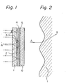
- a photomask comprises a glass substrate 1 having a thickness of 2.:5 mm.
- One surface of the substrate 1 is roughened by sandblasting and the maximum extent of unevenness ranges from 1 to 50 ⁇ m.
- On the other surface of the substrate 1 a line pattern of chromium 2 is formed 0.1 pm in thickness with lines 11.6 pm in width. Minute particles of dust 3 are present on both surfaces of the substrate 1.
- the dust typically has a size or maximum dimension a factor of 10 smaller than the width of the pattern lines.
- the light energy required for the exposure of the photoresist layer 4 has to be increased by about 10% in comparison with a conventional photomask.
- the exposure time required is usually only increased by 1 or 2 seconds. Therefore, the present invention is no more trouble than the conventional method and apparatus used in the photoprocess technique for producing semiconductor devices and, yet is capable of transferring the exact mask pattern without the transfer of images of minute particles of dust. This improves the yield and the reliability of the semiconductor devices so produced.
Landscapes
- Physics & Mathematics (AREA)
- General Physics & Mathematics (AREA)
- Exposure And Positioning Against Photoresist Photosensitive Materials (AREA)
- Preparing Plates And Mask In Photomechanical Process (AREA)
Applications Claiming Priority (2)
| Application Number | Priority Date | Filing Date | Title |
|---|---|---|---|
| JP156206/80 | 1980-10-31 | ||
| JP1980156206U JPS5779848U (de) | 1980-10-31 | 1980-10-31 |
Publications (2)
| Publication Number | Publication Date |
|---|---|
| EP0051402A1 true EP0051402A1 (de) | 1982-05-12 |
| EP0051402B1 EP0051402B1 (de) | 1984-04-25 |
Family
ID=15622681
Family Applications (1)
| Application Number | Title | Priority Date | Filing Date |
|---|---|---|---|
| EP81304970A Expired EP0051402B1 (de) | 1980-10-31 | 1981-10-22 | Photomaske für die - und Verfahren zur - Herstellung von Halbleitervorrichtungen |
Country Status (4)
| Country | Link |
|---|---|
| US (1) | US4402600A (de) |
| EP (1) | EP0051402B1 (de) |
| JP (1) | JPS5779848U (de) |
| DE (1) | DE3163315D1 (de) |
Families Citing this family (5)
| Publication number | Priority date | Publication date | Assignee | Title |
|---|---|---|---|---|
| JPS6197924A (ja) * | 1984-10-19 | 1986-05-16 | Nippon Sheet Glass Co Ltd | 保護カバ− |
| WO1994017449A1 (en) * | 1993-01-21 | 1994-08-04 | Sematech, Inc. | Phase shifting mask structure with multilayer optical coating for improved transmission |
| US5418095A (en) * | 1993-01-21 | 1995-05-23 | Sematech, Inc. | Method of fabricating phase shifters with absorbing/attenuating sidewalls using an additive process |
| US5411824A (en) * | 1993-01-21 | 1995-05-02 | Sematech, Inc. | Phase shifting mask structure with absorbing/attenuating sidewalls for improved imaging |
| TWI254841B (en) * | 2002-12-23 | 2006-05-11 | Asml Netherlands Bv | Lithographic apparatus |
Citations (1)
| Publication number | Priority date | Publication date | Assignee | Title |
|---|---|---|---|---|
| DE2416186A1 (de) * | 1974-04-03 | 1975-10-16 | Siemens Ag | Verfahren zur strukturierung duenner schichten |
Family Cites Families (3)
| Publication number | Priority date | Publication date | Assignee | Title |
|---|---|---|---|---|
| US3507593A (en) * | 1967-05-08 | 1970-04-21 | Tektronix Inc | Contact negative with method and apparatus employing the same |
| NL7200295A (de) * | 1972-01-08 | 1973-07-10 | ||
| JPS6016703Y2 (ja) * | 1981-08-12 | 1985-05-23 | 敏雄 中嶋 | 排水トラップ装置 |
-
1980
- 1980-10-31 JP JP1980156206U patent/JPS5779848U/ja active Pending
-
1981
- 1981-10-22 DE DE8181304970T patent/DE3163315D1/de not_active Expired
- 1981-10-22 EP EP81304970A patent/EP0051402B1/de not_active Expired
- 1981-10-23 US US06/314,429 patent/US4402600A/en not_active Expired - Fee Related
Patent Citations (1)
| Publication number | Priority date | Publication date | Assignee | Title |
|---|---|---|---|---|
| DE2416186A1 (de) * | 1974-04-03 | 1975-10-16 | Siemens Ag | Verfahren zur strukturierung duenner schichten |
Also Published As
| Publication number | Publication date |
|---|---|
| DE3163315D1 (en) | 1984-05-30 |
| JPS5779848U (de) | 1982-05-17 |
| US4402600A (en) | 1983-09-06 |
| EP0051402B1 (de) | 1984-04-25 |
Similar Documents
| Publication | Publication Date | Title |
|---|---|---|
| EP0907105A3 (de) | Verfahren zur Herstellung einer Fotomaske mit einer Phasenschieberschicht | |
| JP3912949B2 (ja) | フォトマスクの形成方法及び半導体装置の製造方法 | |
| JPH0690507B2 (ja) | ホトマスク,及びそれを用いた投影露光方法、並びにホトマスクの製造方法 | |
| EP0051402B1 (de) | Photomaske für die - und Verfahren zur - Herstellung von Halbleitervorrichtungen | |
| JP3177948B2 (ja) | 露光用フォトマスク | |
| US6682858B2 (en) | Method of forming small contact holes using alternative phase shift masks and negative photoresist | |
| JPH1115132A (ja) | ハーフトーン型位相シフトマスク及びハーフトーン型位相シフトマスク用ブランク | |
| US6635394B2 (en) | Three dimensional mask | |
| US5798192A (en) | Structure of a mask for use in a lithography process of a semiconductor fabrication | |
| KR920009369B1 (ko) | 마스크의 제작방법 | |
| JP2878274B2 (ja) | ホトマスクの製造方法 | |
| JP3110801B2 (ja) | フォトマスクの製造方法及びフォトマスク | |
| JPH0664337B2 (ja) | 半導体集積回路用ホトマスク | |
| JPH06105678B2 (ja) | 半導体装置の製造方法 | |
| JP3031728B2 (ja) | レチクルおよび露光装置 | |
| JPS6127548A (ja) | 非接触式露光装置 | |
| JP2892014B2 (ja) | 光露光用マスク及び露光方法 | |
| US20040013948A1 (en) | Chromeless PSM with chrome assistant feature | |
| JP2624335B2 (ja) | レジスト露光方法 | |
| KR0151228B1 (ko) | 고립된 다수의 패턴을 형성하기 위한 포토마스크 | |
| JPS5984245A (ja) | フオトマスク | |
| JPH05275303A (ja) | 露光方法およびそれに用いるフォトマスク | |
| JPH0683036A (ja) | 投影露光用レチクル | |
| JPH05232675A (ja) | ホトマスク及びそれを用いたレジストパターン形成方法 | |
| JPS5720738A (en) | Mask for pattern transfer |
Legal Events
| Date | Code | Title | Description |
|---|---|---|---|
| PUAI | Public reference made under article 153(3) epc to a published international application that has entered the european phase |
Free format text: ORIGINAL CODE: 0009012 |
|
| AK | Designated contracting states |
Designated state(s): DE FR GB NL |
|
| 17P | Request for examination filed |
Effective date: 19820820 |
|
| GRAA | (expected) grant |
Free format text: ORIGINAL CODE: 0009210 |
|
| AK | Designated contracting states |
Designated state(s): DE FR GB NL |
|
| REF | Corresponds to: |
Ref document number: 3163315 Country of ref document: DE Date of ref document: 19840530 |
|
| ET | Fr: translation filed | ||
| PLBE | No opposition filed within time limit |
Free format text: ORIGINAL CODE: 0009261 |
|
| STAA | Information on the status of an ep patent application or granted ep patent |
Free format text: STATUS: NO OPPOSITION FILED WITHIN TIME LIMIT |
|
| 26N | No opposition filed | ||
| PGFP | Annual fee paid to national office [announced via postgrant information from national office to epo] |
Ref country code: GB Payment date: 19921012 Year of fee payment: 12 |
|
| PGFP | Annual fee paid to national office [announced via postgrant information from national office to epo] |
Ref country code: FR Payment date: 19921028 Year of fee payment: 12 |
|
| PGFP | Annual fee paid to national office [announced via postgrant information from national office to epo] |
Ref country code: NL Payment date: 19921031 Year of fee payment: 12 |
|
| PGFP | Annual fee paid to national office [announced via postgrant information from national office to epo] |
Ref country code: DE Payment date: 19921226 Year of fee payment: 12 |
|
| PG25 | Lapsed in a contracting state [announced via postgrant information from national office to epo] |
Ref country code: GB Effective date: 19931022 |
|
| PG25 | Lapsed in a contracting state [announced via postgrant information from national office to epo] |
Ref country code: NL Effective date: 19940501 |
|
| NLV4 | Nl: lapsed or anulled due to non-payment of the annual fee | ||
| GBPC | Gb: european patent ceased through non-payment of renewal fee |
Effective date: 19931022 |
|
| PG25 | Lapsed in a contracting state [announced via postgrant information from national office to epo] |
Ref country code: FR Effective date: 19940630 |
|
| PG25 | Lapsed in a contracting state [announced via postgrant information from national office to epo] |
Ref country code: DE Effective date: 19940701 |
|
| REG | Reference to a national code |
Ref country code: FR Ref legal event code: ST |