EP0048057B1 - Schaltungsanordnung zur Modulation des Ausgangssignals eines Wandlers, z.B. eines elektrooptischen Wandlers - Google Patents
Schaltungsanordnung zur Modulation des Ausgangssignals eines Wandlers, z.B. eines elektrooptischen Wandlers Download PDFInfo
- Publication number
- EP0048057B1 EP0048057B1 EP81200992A EP81200992A EP0048057B1 EP 0048057 B1 EP0048057 B1 EP 0048057B1 EP 81200992 A EP81200992 A EP 81200992A EP 81200992 A EP81200992 A EP 81200992A EP 0048057 B1 EP0048057 B1 EP 0048057B1
- Authority
- EP
- European Patent Office
- Prior art keywords
- signal
- converter
- output signal
- arrangement
- limiter
- Prior art date
- Legal status (The legal status is an assumption and is not a legal conclusion. Google has not performed a legal analysis and makes no representation as to the accuracy of the status listed.)
- Expired
Links
- 230000010355 oscillation Effects 0.000 claims description 10
- 239000004065 semiconductor Substances 0.000 claims description 7
- 230000000903 blocking effect Effects 0.000 claims description 6
- 230000001419 dependent effect Effects 0.000 claims description 5
- 238000001514 detection method Methods 0.000 claims 1
- 230000003287 optical effect Effects 0.000 description 12
- 239000003990 capacitor Substances 0.000 description 4
- 238000001228 spectrum Methods 0.000 description 4
- 230000005540 biological transmission Effects 0.000 description 3
- 239000000835 fiber Substances 0.000 description 3
- 238000010586 diagram Methods 0.000 description 2
- 238000005259 measurement Methods 0.000 description 2
- 230000006978 adaptation Effects 0.000 description 1
- 238000006243 chemical reaction Methods 0.000 description 1
- 230000001934 delay Effects 0.000 description 1
- 230000008034 disappearance Effects 0.000 description 1
- 230000000694 effects Effects 0.000 description 1
- 239000013307 optical fiber Substances 0.000 description 1
- 230000010363 phase shift Effects 0.000 description 1
- 230000008054 signal transmission Effects 0.000 description 1
- 230000001629 suppression Effects 0.000 description 1
Images

Classifications
-
- H—ELECTRICITY
- H04—ELECTRIC COMMUNICATION TECHNIQUE
- H04B—TRANSMISSION
- H04B14/00—Transmission systems not characterised by the medium used for transmission
- H04B14/02—Transmission systems not characterised by the medium used for transmission characterised by the use of pulse modulation
- H04B14/026—Transmission systems not characterised by the medium used for transmission characterised by the use of pulse modulation using pulse time characteristics modulation, e.g. width, position, interval
-
- H—ELECTRICITY
- H01—ELECTRIC ELEMENTS
- H01S—DEVICES USING THE PROCESS OF LIGHT AMPLIFICATION BY STIMULATED EMISSION OF RADIATION [LASER] TO AMPLIFY OR GENERATE LIGHT; DEVICES USING STIMULATED EMISSION OF ELECTROMAGNETIC RADIATION IN WAVE RANGES OTHER THAN OPTICAL
- H01S5/00—Semiconductor lasers
- H01S5/06—Arrangements for controlling the laser output parameters, e.g. by operating on the active medium
- H01S5/068—Stabilisation of laser output parameters
- H01S5/0683—Stabilisation of laser output parameters by monitoring the optical output parameters
- H01S5/06835—Stabilising during pulse modulation or generation
-
- H—ELECTRICITY
- H03—ELECTRONIC CIRCUITRY
- H03C—MODULATION
- H03C3/00—Angle modulation
- H03C3/36—Angle modulation by means of light-sensitive element
-
- H—ELECTRICITY
- H04—ELECTRIC COMMUNICATION TECHNIQUE
- H04B—TRANSMISSION
- H04B10/00—Transmission systems employing electromagnetic waves other than radio-waves, e.g. infrared, visible or ultraviolet light, or employing corpuscular radiation, e.g. quantum communication
- H04B10/50—Transmitters
- H04B10/501—Structural aspects
- H04B10/503—Laser transmitters
- H04B10/504—Laser transmitters using direct modulation
-
- H—ELECTRICITY
- H04—ELECTRIC COMMUNICATION TECHNIQUE
- H04B—TRANSMISSION
- H04B10/00—Transmission systems employing electromagnetic waves other than radio-waves, e.g. infrared, visible or ultraviolet light, or employing corpuscular radiation, e.g. quantum communication
- H04B10/50—Transmitters
- H04B10/564—Power control
Definitions
- the invention relates to an arrangement for modulating the output signal of a converter converting electric signals into other signals, for example of an electro-optical converter such as a semiconductor laser diode with an analog input signal, the arrangement comprising a negative feedback loop in which the converter is included, comprising means for demodulating a portion of the converter output signal for supplying a feedback signal and means for applying the feedback signal and the analog input signal to a difference producer in which the feedback signal is subtracted from the analog input signal.
- an electro-optical converter such as a semiconductor laser diode with an analog input signal
- the arrangement comprising a negative feedback loop in which the converter is included, comprising means for demodulating a portion of the converter output signal for supplying a feedback signal and means for applying the feedback signal and the analog input signal to a difference producer in which the feedback signal is subtracted from the analog input signal.
- optical feedback proposed therein is of necessity limited to a small frequency bandwidth and/or a low loop gain in view of the risk of instability of the feedback loop due to the delays and phase shifts occurring therein.
- the invention has for its object to realize a linear modulation of the converter output signal as well as a high signal-to-noise ratio of the modulated output signal.
- this object is accomplished in that the output signal of the difference producer controls a limiter, the limiter producing a binary output signal for controlling the said converter, all this in such manner that a self-excited oscillation is obtained with an analog-signal dependent modulation in the negative feedback loop of the pulse width and/or pulse density of the pulse-shaped output signal of the limiter.
- the non-linear distortion products of the modulating analog signal which are present in the modulated output signal and are the result of a non-linear conversion characteristic of the converter and/or the non-linearity in the switching delay of the converter, and the noise and the signal-dependent pulse amplitude variation produced at the output of the converter are compensated for a considerable portion by an instantaneous adaptation of the pulse width/pulse period ratio of the limiter output signal.
- a modulation system which is designated rectangular wave modulation, in, inter alia, Electronics Letters, January 1966, Volume 2, Nn. 1, pages 7-9, the information signal being applied to a difference producer the output signal of which controls a limiter, means being present for applying a portion of the limiter output signal to the difference producer, all this in such manner that a self-excited oscillation is obtained with an information signal-dependent modulation of the pulse density and the pulse width of the pulse-shaped output signal of the limiter.
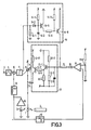
- the modulation arrangement of Figure 1 comprises a semiconductor diode laser 1, which is coupled to an optical fibre 2 and a photo-sensitive detector 3.
- An analog signal which is in this case, for example, a television video signal is applied to a signal input 4.
- This signal is clamped in a clamping circuit 5 onto a fixed synchronizing pulse level.
- the clamping circuit may comprise in known manner a capacitor in series, with the parallel circuit of a resistor and a diode connected between a pair of input terminals, the output being derived from across the parallel circuit.
- the output signal of the clamping circuit 5 is applied to a difference producer 6, in which a negative feedback signal is subtracted from the video signal.
- the output signal of the difference producer 6 controls a symmetrical limiter 7, which produces a binary output signal the value of which depends on the polarity of the input signal with respect to a discrimination level.
- the binary output signal of the limiter 7 controls an adjustable current source 8 for the signal current Is, which is applied to the semiconductor laser diode 1.
- the photo-sensitive diode 3 is connected to the input of a broadband amplifier 9 the output of which is connected to a peak value detector 10, the output signal of which is a measure of the optical peak power of the laser diode 1.
- This output signal is applied to the inverting input of a difference voltage amplifier 11.
- a reference voltage Vref which is a measure of the desired optical peak power is applied to the noninverting input of this difference voltage amplifier.
- the output signal of amplifier 11 controls an adjustable current source 12 for the basis current Ib, which is applied to the laser diode 1. This control adjusts the optical peak power to a desired value by adjusting the bias current lb.
- the output of amplifier 9 is connected to the difference producer 6 through an integrator 13. This closes a negative feedback loop which comprises the circuit elements 6-7-8-1-3-9-13-6.
- This negative feedback loop has a large bandwidth and a high gain in order to realize a large negative feedback factor over a wide frequency range.
- a copy of the analog input signal will be produced at the output of the integrator 13 and any difference from the analog input signal will effect a change in the pulse width/pulse period ratio of the pulse-shaped output signal of the limiter 7, thereby reducing the difference.
- the negative feedback loop has such a bandwidth and such a high gain that self-excited oscillation is produced at a high frequency.
- the negative feedback loop oscillated without input signal at a frequency of 25 MHz.
- the input signal modulates both the pulse density and the pulse width of the output signal of limiter 7.
- the pulse repetition rate varied between 15 MHz and 25 MHz. This combined modulation results in a frequency spectrum in which the basic frequency band of the analog signal has a relatively high power, so that this system is very suitable for transmission over a fibre having a relatively small bandwidth, such as a "step-index" fibre.
- the negative feedback of the baseband signal furnishes considerable advantages as regards the linearity of the modulation and the suppression of noise, particularly the noise produced in the optical output signal of the laser diode 1 by the optical retroaction of fibre 2 on the laser diode 1.
- the waveform of the optical signal will influence the signal transmission to a lesser extent, as signal variations due to the waveform will be fed back and reduced by the negative feedback factor.
- Fig. 2 shows some curves which are based on measurements made with a spectrum analyser when a system having direct intensity modulation (curve B) and a system having a modulation arrangement of Fig. 1 (curve C) are compared.
- the measurements were made on the demodulated optical signal in the case of transmission of a 2 MHz sinusoidal signal the spectrum of which is illustrated by curve A.
- the bias current of the laser diode has been adjusted for minimum signal distortion and the signal current was adjusted for obtaining the same signal strength of the demodulated signal as in the system of the invention.
- the noise level is reduced by approximately 12 dB and the second and third harmonics of the signal are each reduced by approximately 10 dB.
- limiter 7 remains in the position in which the value of the signal current Is is low (zero).
- the control loop which comprises peak detector 10 and amplifier 11 will try to keep the optical peak power constant. If thereafter the self-excited oscillation of the feedback loop starts then the bias current Ib is adjusted to a value which is much too high and the laser diode 1 must handle too high a current.
- a blocking device 14 is provided in the modulation arrangement of Fig. 3 to detect the disappearance of the self-excited oscillation of the negative feedback loop and to provide a blocking signal in the absence of the self-excited oscillation to block the bias current.
- the blocking device 14 comprises a peak detector, including a resistor 14-1, a diode 14-2 and a capacitor 14-3, which is connected to the inverse output of the limiter 7.
- a peak detector including a resistor 14-1, a diode 14-2 and a capacitor 14-3, which is connected to the inverse output of the limiter 7.
- transistor 14-5 causes a current to flow through the resistor 14-6 and the resistor 14-7, as a result of which the transistor 14-8 starts carrying current.
- This current is derived from the input of the controllable current source 12, which input is connected to the output of amplifier 11 through a resistor 15 and a diode 16 which are arranged in series.
- the controllable current source 12 comprises an input stage which includes a transistor 12-1 and the bias resistors 12-2 and 12-3 and an emitter load resistor 12-4.
- a capacitor 12-5 which can be discharged by the collector current of transistor 14-8 in such manner that transistor 12-1 is cut-off is arranged between the base of the transistor 12-1 and the negative supply voltage.
- blocked transistor 12-1 cannot pass a control current through the resistor 12-6 to the final stage which comprises the transistor 12-7 and the emitter load resistor 12-8. Then the collector of transistor 12-7 cannot apply a bias current Ib to the laser diode 1.
- the diode 16 is blocked when transistor 14-8 starts carrying current, as a result of which the normal control of the bias current Ib by the output signal of amplifier 11 is interrupted.
- transistors 14-5 and 14-8 are cut-off and the normal control of the bias current Ib can become operative.
- the adjustable current source 8 can be implemented in the same manner as the adjustable current source 12, the details of which are shown in Fig. 3.
- the invention is not limited to use in electro-optical converters. It can also be used in connection with, for example, electro-acoustic converters such as loudspeakers, it being then possible to reduce the influence of non-linearities on the acoustic output signal.
Landscapes
- Physics & Mathematics (AREA)
- Electromagnetism (AREA)
- Engineering & Computer Science (AREA)
- Computer Networks & Wireless Communication (AREA)
- Signal Processing (AREA)
- Optics & Photonics (AREA)
- Condensed Matter Physics & Semiconductors (AREA)
- General Physics & Mathematics (AREA)
- Semiconductor Lasers (AREA)
- Optical Communication System (AREA)
Claims (3)
Applications Claiming Priority (2)
| Application Number | Priority Date | Filing Date | Title |
|---|---|---|---|
| NL8005153A NL8005153A (nl) | 1980-09-15 | 1980-09-15 | Inrichting voor het moduleren van het uitgangssignaal van een omzetter, bijvoorbeeld een electro-optische omzetter. |
| NL8005153 | 1980-09-15 |
Publications (2)
| Publication Number | Publication Date |
|---|---|
| EP0048057A1 EP0048057A1 (de) | 1982-03-24 |
| EP0048057B1 true EP0048057B1 (de) | 1984-04-25 |
Family
ID=19835881
Family Applications (1)
| Application Number | Title | Priority Date | Filing Date |
|---|---|---|---|
| EP81200992A Expired EP0048057B1 (de) | 1980-09-15 | 1981-09-08 | Schaltungsanordnung zur Modulation des Ausgangssignals eines Wandlers, z.B. eines elektrooptischen Wandlers |
Country Status (7)
| Country | Link |
|---|---|
| US (1) | US4450564A (de) |
| EP (1) | EP0048057B1 (de) |
| JP (1) | JPS5781739A (de) |
| AU (1) | AU543244B2 (de) |
| CA (1) | CA1186379A (de) |
| DE (1) | DE3163309D1 (de) |
| NL (1) | NL8005153A (de) |
Families Citing this family (14)
| Publication number | Priority date | Publication date | Assignee | Title |
|---|---|---|---|---|
| JPS57162481A (en) * | 1981-03-23 | 1982-10-06 | Ibm | Control circuit for light emtting semiconductor device |
| JPS59146457A (ja) * | 1983-02-10 | 1984-08-22 | Olympus Optical Co Ltd | 光出力自動制御装置 |
| JPS59182637A (ja) * | 1983-03-31 | 1984-10-17 | Matsushita Electric Ind Co Ltd | ビデオ信号光伝送装置 |
| US4621376A (en) * | 1983-04-28 | 1986-11-04 | Kabushiki Kaisha Toshiba | Driving apparatus for stabilizing burst light output |
| CA1251845A (en) * | 1984-08-06 | 1989-03-28 | Ian D. Henning | Optical amplification |
| US4625315A (en) * | 1984-08-27 | 1986-11-25 | Minnesota Mining And Manufacturing Company | Apparatus and circuitry for stabilizing laser diode output for analog modulation |
| DE3431996A1 (de) * | 1984-08-31 | 1986-03-13 | Fa. Carl Zeiss, 7920 Heidenheim | Stromversorgung fuer strahlungsquellen von frequenz-analogen optischen sensoren |
| US4733398A (en) * | 1985-09-30 | 1988-03-22 | Kabushiki Kaisha Tohsiba | Apparatus for stabilizing the optical output power of a semiconductor laser |
| DE3750030T2 (de) * | 1986-12-29 | 1994-09-29 | Fuji Photo Film Co Ltd | Laserstrahlaufzeichnungsverfahren und -vorrichtung. |
| US4774710A (en) * | 1988-01-07 | 1988-09-27 | Eastman Kodak Company | Apparatus and method for controlling a laser diode to generate a linear illuminative output |
| US5128950A (en) * | 1989-08-02 | 1992-07-07 | Hamamatsu Photonics K.K. | Low noise pulsed light source using laser diode |
| US5179565A (en) * | 1990-06-07 | 1993-01-12 | Hamamatsu Photonics, K.K. | Low noise pulsed light source utilizing laser diode and voltage detector device utilizing same low noise pulsed light source |
| AU682982B2 (en) * | 1994-09-14 | 1997-10-23 | Wood Nang Cheung | A low noise photon coupled circuit |
| CN101431850B (zh) * | 2008-12-10 | 2012-11-07 | 上海亚明灯泡厂有限公司 | 一种用于陶瓷金卤灯电子镇流器的简易Buck电路 |
Family Cites Families (5)
| Publication number | Priority date | Publication date | Assignee | Title |
|---|---|---|---|---|
| US3258596A (en) * | 1966-06-28 | Pulse-frequency modulated injection laser | ||
| IT1160592B (it) * | 1978-08-16 | 1987-03-11 | Cselt Centro Studi Lab Telecom | Procedimento e sistema di controllo dell'efficienza di un dispositivo elettronico |
| DE2911858C2 (de) * | 1979-03-26 | 1983-01-13 | Robert Bosch Gmbh, 7000 Stuttgart | Schaltung zur Begrenzung der von einem Halbleiterlaser abgegebenen Lichtleistung |
| US4305047A (en) * | 1979-10-09 | 1981-12-08 | Digital Communications Corp. | Feedback circuit for controlling the peak optical output power of an injection laser |
| NL7907683A (nl) * | 1979-10-18 | 1981-04-22 | Philips Nv | Regelketen voor de bekrachtigingsstroom van een laser. |
-
1980
- 1980-09-15 NL NL8005153A patent/NL8005153A/nl not_active Application Discontinuation
-
1981
- 1981-09-04 US US06/299,436 patent/US4450564A/en not_active Expired - Fee Related
- 1981-09-08 EP EP81200992A patent/EP0048057B1/de not_active Expired
- 1981-09-08 CA CA000385336A patent/CA1186379A/en not_active Expired
- 1981-09-08 DE DE8181200992T patent/DE3163309D1/de not_active Expired
- 1981-09-12 JP JP56143191A patent/JPS5781739A/ja active Pending
- 1981-09-14 AU AU75215/81A patent/AU543244B2/en not_active Ceased
Also Published As
| Publication number | Publication date |
|---|---|
| AU7521581A (en) | 1982-03-25 |
| JPS5781739A (en) | 1982-05-21 |
| US4450564A (en) | 1984-05-22 |
| DE3163309D1 (en) | 1984-05-30 |
| EP0048057A1 (de) | 1982-03-24 |
| AU543244B2 (en) | 1985-04-04 |
| CA1186379A (en) | 1985-04-30 |
| NL8005153A (nl) | 1982-04-01 |
Similar Documents
| Publication | Publication Date | Title |
|---|---|---|
| US4347610A (en) | Control circuit for the drive current of a laser | |
| EP0048057B1 (de) | Schaltungsanordnung zur Modulation des Ausgangssignals eines Wandlers, z.B. eines elektrooptischen Wandlers | |
| US5054116A (en) | Feed-forward automatic level control circuit for a high-frequency source | |
| CA2106439A1 (en) | Burst mode digital data receiver | |
| GB2258561A (en) | Apparatus and method for controlling a laser diode. | |
| JPH0210615B2 (de) | ||
| US5187713A (en) | Nonlinear device control methods and apparatus | |
| JPH02113640A (ja) | 自動利得制御装置 | |
| US20070230967A1 (en) | Optical transmission system | |
| US6163212A (en) | Power amplifier system | |
| US5293263A (en) | Electro-optical modulator which provides optical bias stabilization during operation | |
| JPH0254695B2 (de) | ||
| JPS6047782B2 (ja) | 発光素子出力安定化回路 | |
| JP2953799B2 (ja) | 光受信回路 | |
| JPH03175709A (ja) | 高周波増幅器の電力制御回路 | |
| JPH0329211B2 (de) | ||
| JPH0563647A (ja) | 光送信装置 | |
| JPS60264130A (ja) | レ−ザダイオ−ド駆動回路 | |
| JPH05206559A (ja) | 光半導体変調装置 | |
| JPH03149925A (ja) | リニア変調無線送信装置 | |
| JPS6136604B2 (de) | ||
| JPS62145905A (ja) | 変調器 | |
| JPS5841675B2 (ja) | 光アナログ信号変調方式 | |
| JPS601937A (ja) | パルス化fm信号の光変換回路 | |
| JPS63316579A (ja) | ビデオ信号発生装置 |
Legal Events
| Date | Code | Title | Description |
|---|---|---|---|
| PUAI | Public reference made under article 153(3) epc to a published international application that has entered the european phase |
Free format text: ORIGINAL CODE: 0009012 |
|
| AK | Designated contracting states |
Designated state(s): BE DE FR GB IT NL SE |
|
| 17P | Request for examination filed |
Effective date: 19820705 |
|
| RAP1 | Party data changed (applicant data changed or rights of an application transferred) |
Owner name: N.V. PHILIPS' GLOEILAMPENFABRIEKEN |
|
| ITF | It: translation for a ep patent filed | ||
| GRAA | (expected) grant |
Free format text: ORIGINAL CODE: 0009210 |
|
| AK | Designated contracting states |
Designated state(s): BE DE FR GB IT NL SE |
|
| REF | Corresponds to: |
Ref document number: 3163309 Country of ref document: DE Date of ref document: 19840530 |
|
| ET | Fr: translation filed | ||
| PLBE | No opposition filed within time limit |
Free format text: ORIGINAL CODE: 0009261 |
|
| STAA | Information on the status of an ep patent application or granted ep patent |
Free format text: STATUS: NO OPPOSITION FILED WITHIN TIME LIMIT |
|
| 26N | No opposition filed | ||
| PGFP | Annual fee paid to national office [announced via postgrant information from national office to epo] |
Ref country code: GB Payment date: 19930827 Year of fee payment: 13 |
|
| PGFP | Annual fee paid to national office [announced via postgrant information from national office to epo] |
Ref country code: BE Payment date: 19930909 Year of fee payment: 13 |
|
| PGFP | Annual fee paid to national office [announced via postgrant information from national office to epo] |
Ref country code: FR Payment date: 19930922 Year of fee payment: 13 |
|
| PGFP | Annual fee paid to national office [announced via postgrant information from national office to epo] |
Ref country code: SE Payment date: 19930927 Year of fee payment: 13 |
|
| ITTA | It: last paid annual fee | ||
| PGFP | Annual fee paid to national office [announced via postgrant information from national office to epo] |
Ref country code: NL Payment date: 19930930 Year of fee payment: 13 |
|
| PGFP | Annual fee paid to national office [announced via postgrant information from national office to epo] |
Ref country code: DE Payment date: 19931129 Year of fee payment: 13 |
|
| PG25 | Lapsed in a contracting state [announced via postgrant information from national office to epo] |
Ref country code: GB Effective date: 19940908 |
|
| PG25 | Lapsed in a contracting state [announced via postgrant information from national office to epo] |
Ref country code: SE Effective date: 19940909 |
|
| PG25 | Lapsed in a contracting state [announced via postgrant information from national office to epo] |
Ref country code: BE Effective date: 19940930 |
|
| EAL | Se: european patent in force in sweden |
Ref document number: 81200992.6 |
|
| BERE | Be: lapsed |
Owner name: N.V. PHILIPS' GLOEILAMPENFABRIEKEN Effective date: 19940930 |
|
| PG25 | Lapsed in a contracting state [announced via postgrant information from national office to epo] |
Ref country code: NL Effective date: 19950401 |
|
| GBPC | Gb: european patent ceased through non-payment of renewal fee |
Effective date: 19940908 |
|
| NLV4 | Nl: lapsed or anulled due to non-payment of the annual fee | ||
| PG25 | Lapsed in a contracting state [announced via postgrant information from national office to epo] |
Ref country code: FR Effective date: 19950531 |
|
| PG25 | Lapsed in a contracting state [announced via postgrant information from national office to epo] |
Ref country code: DE Effective date: 19950601 |
|
| EUG | Se: european patent has lapsed |
Ref document number: 81200992.6 |
|
| REG | Reference to a national code |
Ref country code: FR Ref legal event code: ST |