EP0045467A1 - Appareil de visualisation d'images - Google Patents
Appareil de visualisation d'images Download PDFInfo
- Publication number
- EP0045467A1 EP0045467A1 EP81105920A EP81105920A EP0045467A1 EP 0045467 A1 EP0045467 A1 EP 0045467A1 EP 81105920 A EP81105920 A EP 81105920A EP 81105920 A EP81105920 A EP 81105920A EP 0045467 A1 EP0045467 A1 EP 0045467A1
- Authority
- EP
- European Patent Office
- Prior art keywords
- electrodes
- image display
- picture image
- disposed
- deflection
- Prior art date
- Legal status (The legal status is an assumption and is not a legal conclusion. Google has not performed a legal analysis and makes no representation as to the accuracy of the status listed.)
- Granted
Links
Images


Classifications
-
- H—ELECTRICITY
- H01—ELECTRIC ELEMENTS
- H01J—ELECTRIC DISCHARGE TUBES OR DISCHARGE LAMPS
- H01J31/00—Cathode ray tubes; Electron beam tubes
- H01J31/08—Cathode ray tubes; Electron beam tubes having a screen on or from which an image or pattern is formed, picked up, converted, or stored
- H01J31/10—Image or pattern display tubes, i.e. having electrical input and optical output; Flying-spot tubes for scanning purposes
- H01J31/12—Image or pattern display tubes, i.e. having electrical input and optical output; Flying-spot tubes for scanning purposes with luminescent screen
- H01J31/123—Flat display tubes
- H01J31/125—Flat display tubes provided with control means permitting the electron beam to reach selected parts of the screen, e.g. digital selection
- H01J31/126—Flat display tubes provided with control means permitting the electron beam to reach selected parts of the screen, e.g. digital selection using line sources
-
- H—ELECTRICITY
- H01—ELECTRIC ELEMENTS
- H01J—ELECTRIC DISCHARGE TUBES OR DISCHARGE LAMPS
- H01J2329/00—Electron emission display panels, e.g. field emission display panels
- H01J2329/86—Vessels
- H01J2329/8625—Spacing members
Definitions
- the present invention relates to an improvement of a multiple electron beam type flat picture image display apparatus and especially concerns the picture image display apparatus having a novel structure capable of reducing distorsion of image and reducing the sizes of electron beam spots thereby assuring high quality image display.
- FIG. 1 is an exploded view of the principal part of the apparatus.
- M predetermined number
- linear thermionic cathodes 1 i.e., line cathodes, each of which comprises a linear filament line to be heated by a low voltage, e.g., D.C.
- the number N of the vertical sections is 107
- the number n of picture element in each section is 3.
- 107 beam spots are produced from each linear thermionic cathode and 107 control electrodes are provided in order to control the 107 electron beam intensities.
- the horizontal scanning is made by using, for instance, saw-tooth wave having a horizontal scanning period H applied to the horizontal deflection electrode and in a manner that all the N beam spots are deflected simultaneously to scan in the same direction taking one horizontal scanning period H.
- the horizontal scanning period H is equal to the horizontal scanning period of the ordinary time sequential television signal.
- the ordinary time sequential image signal is preliminarily converted into the N parallel signals of the line-at-a-time type.
- the vertical scanning of the described apparatus is made by dividing the raster into a plural number M of horizontally oblong sections, and at first in the first section, for example in the uppermost section, the plural number of beam spots, which simultaneously scan, also scan vertically (downwards).
- the vertical scanning in the first section is over and all the beam spots reach the bottoms of the first horizontally oblong sections, then the forming of electron beams from the electron from the first linear thermionic cathods ends and the forming of electron beams from the electrons from the second linear thermionic cathode starts, and the vertical scannings of the beam spots start in the second horizontally oblong section and scan downwards in the same way as in the first section.
- the vertical scanning is made thus downwards to the bottom or M-th section by, for instance, applying a saw-tooth wave having a period , where V is the vertical scanning period of the ordinary television signal.
- V is the vertical scanning period of the ordinary television signal.
- the electron beams taken out from the apertures 3a of the extractor electrode 3 are first controlled of their density and then are deflected vertically and horizontally.
- the image formed on the phosphor screen is subject to distortions of barrel form or pin-cushion type and, etc. Therefore, not only the reproduced image is distorted, but also the scanning spot is not sufficiently focussed, thus the size of the spot cannot be made smaller than 0.3mm. Furthermore, a considerably large energy was necessary for the vertical scanning in each of the vertically divided regions.
- the present invention purports to provide an improved picture image apparatus capable of attaining small distortions in scanning and smallness of scanning spots on the image, and higher efficiency of vertical scanning power.
- a picture image display apparatus in accordance with the present invention comprises.a flat type vacuum enclosure having a transparent face panel containing therein the followings disposed in the following order:
- FIG. 2 shows an example of structural configuration of a picture image apparatus in accordance with the present invention.
- FIG. 2 is an exploded view which shows a very small part of the apparatus and
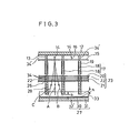
- FIG. 3 is a plan view of a small part of the apparatus shown in FIG. 2.
- the whole apparatus comprises many repetitions of the segments shown in FIGs. 2 and 3 in vertical and horizontal directions of the face panel 12'.
- a flat type vacuum enclosure 12 contains various components therein.
- the vacuum enclosure 12 is a flat box-shaped enclosure made of glass.
- a back face electrode 13 is formed on the inner face of a back face of the vacuum enclosure by known vacuum deposition of aluminum.
- a plural of linear cathode electrodes 14 are made by coating electron-emissive oxide on 10 to 20 ⁇ m diameter tungsten wires and the linear cathode electrodes14 are disposed parallelly to each other and with a predetermined pitch substantially on a plane parallel to said back face electrode 13.
- An electron extracting electrode 15 or a first grid having electron passing through-openings 16 is made with a metal sheet disposed substantially parallel to the plane of disposition of the linear cathodes 14.
- the through-openings 16 are, for instance, linear slits disposed in parallel row in a manner that the electron beams from respective linear cathodes 14 passes through the openings 16 perpendicularly to the face of the electron extracting electrode 15.
- the linear slits 16 can be made in segments of slits, i.e. with reinforcing interruption therein like a interrupted slits in chain line rule.
- a first deflection electrodes 17 is disposed next to the- electron extracting- electrode.
- the first deflection electrode is for vertical deflection with respect to display image and comprises a parallel row of strip shaped conductors 19 formed on both faces of substrates 18 which are disposed each other parallel and parallel to said linear cathodes 14, face of the substractes 18 being substantially perpendicular to the electron-extracting electrode 15.
- Each pair of conductors 19 opposing each other with electron beam passing space inbetween forms a vertical deflection electrode pair, wherein a vertical deflection voltage, for instance, a saw-tooth voltage is impressed across the conductors 19 of the pair so that the electron beam extracted through the slit 16 receives deflection power of the direction perpendicular to the face of the conductors 19.
- the control means 23 comprises a second grid 20, a row of control electrodes 25, and a third.grid.21 in this order.
- the second . grid 20 has a number of slits 24 perdendicular to the plane of the conductors. 19 and also has several engaging means for engaging with the substrates 18.
- the strip shaped control electrodes 22 are disposed paralleley to each other on a plane parallel to the second grid 20, and parallelly to and facing the slits 24, and each has slits 25.
- the third grid 21 is disposed parallelly to the second grid 20 and has slits at positions corresponding to those of the slits 24.
- a second deflection means 26 comprising a number of electrodes 26a for horizontal deflection with respect to display image are disposed.
- the second deflection electrodes 26a are disposed in a manner that deflection spaces defined between a pair of neighboring deflection electrodes 26a are disposed under the slits 24 and 25.
- Horizontal deflection voltage for instance, a saw-tooth voltage is impressed across the pair of neighboring electrodes 26a.
- a phosphor screen 30 is formed on a front face panel of the vacuum enclosure 12, and an anode 31 of thin metal film formed by vapor deposition of aluminum is formed on the phosphor screen 30.
- a space between the second deflection means 26 and the anode 31 may be left empty for a relatively small sized display apparatus.
- the acceleration means comprises a row of insulator boards 29 of glass or ceramic and serves as substrate for accelerator electrode as well as reinforcing frames for holding the inner face of the face panel 12.
- the insulator boards 29 are disposed parallelly to each other and perpendicularly to the face panel 12'.
- spacers 34 are disposed between the electordes 20, 22 and 21, and another spacer 34' are disposed between the first grid 15 and the back face of the enclosure 12, so that the electrode assembly cooperatingly supports the back face 12 and the face panel 12' against large air pressure.
- These reinforcing spacers 34 and 34' are omitted in FIG.2 for simplicity of illustration.
- a wider stripe electorde 38 is provided on each substrate at the part nearer to the face panel 12', and narrower stripe electrodes 39a, 39b, 39c and 39d are provided on each substrate at the part nearer to the second deflection means 26.
- the wider stripe electrodes 38 impressed with substantially the same potential to that of the anode 31.
- the narrower stripe electrodes 39a to 39d can be left unconnected to a particular potential.
- the wider stripe electrodes 38 form a row of accelerating electrodes, and in each segment formed by a pair of opposing wider stripe electrodes 38, the pair forms, together with the anode 31,an electric field having equipotential faces with sections like catenary curves between the upper edges of the wider stripe electrodes 38.
- the row of insulator boards 29 with the acceleration electrodes 38 is held by frames 33 made of metal sheet disposed on the anode, so that a rigid structure is formed to hold the face panel 12' against atmospheric pressure.
- a hypothetical plane connecting the linear.cathode 14 and the slit shaped through-opening 16 on the first grid 15 is disposed at the center position between each-other facing pair _of the vertical deflection electrodes 19, 19 and between each-other facing pair of the acceleration electrodes 38, 38, so that the electron beam can be deflected either way of paths C and B (corresponding to upwards and downwards) from the non-deflected central position A.
- the beam A is for the case where voltages of both of electrodes 19, 19 are the same
- C is the case where voltage of the left side one of the vertical deflection electrode is higher than that of the right side one
- B is the case where the voltage of the right side one of the vertical deflection electrode is higher than that of the left side one.
- the positionings of the substrates 29 are made accurate, and furthermore, by suitably selecting height "h" of the frame 33, a defect of forming undesirable shadows of electron beam due to the thickness of the substrate 29 and the acceleration electrodes 38 thereon can be eliminated.
- a beautiful image display substantially without any shadow of the frames or insulation boards 29 is obtainable.
- the preferable mode of the acceleration electrode is that as shown in FIG. 4(a), a wider stripe shape electrode 38 is disposed at the part nearer to the anode and a predetermined number of parallel narrower stripe shape electrodes 39a to 39d are disposed at the part nearer to the second deflection mean.
- the parallel narrower stripe shaped electrodes 39a to 39d on the insulation boards serve to prevent undesirable local concentration of electric charges on the surface of the insulation boards.
- the wider stripe shape electrode 38 serves to form an electric field having catenary shaped :equipotential faces, and the narrower stripe shape electrodes serves to prevent undersirable non-uniformity of electric field due to irregular local deposition of electron charges.
- the potentials of the narrower stripe shape electrodes 39a to 39d are supposed to orderly distributes from the high potential of the anode to which the wider stripe shaped electrode 38 is usualy connected and to a very low potential of the second deflection means. It is experimentally confirmed that 30% or more of the area of the insulator board 29 should be covered by such electrodes, so that undesirable effect of electron charge accumulation on the insulator boards 29.
- high resistance resistors 40 such as 1000 M ⁇ or more may be connected as shown by dotted lines in FIG. 4(a).
- FIG. 4 (b) shows another example where a wire resistor 39e of very high resistance is connected in a zigzag way between the upper end narrower electrode 39d and the lower end wider electrode 38.
- the resistance of the extended wire resistor 39e should be very high, for instance 100M ⁇ or more, in order to save waste of current therethrough.
- the effect of the post stage acceleration means 28 is boosting of the first (vertical) deflection. This is elucidated by that the electric field of catenary shaped or downward concave equipotential face give the effect of boosting the vertical deflection. Therefore, an effective vertical deflection with a small deflection power becomes possible.
- potential of -20V (pulse) on the linear cathode 14 potential of +10V on the first grid 15, potential of 0V as the basic potential on the first (vertical) deflection means and potential of +130V on the second grid 20
- the width of the electron beam spot on the phosphor screan 30 (which is in the direction with wise of FIG. 3) can be focussed to 0.1mm or smaller, and the width does not substantially change, thereby assuring a high resolution.
- the smallness of the spot is not spoiled even when defelected to the limit of the deflections B and C of FIG. 3.
- the second (horizontal) deflection means 26 is exposed directly to the underlying high electric field of the electron beam acceleration, and the electron beam is focussed in the direction perpendicular to the paper of FIG. 3, by an electric field lens whose characteristic is defined by pitch of the electrodes 26a and intensity of the acceleration electric field thereunder on the phosphor screen 30.
- the focussing condition By suitably selecting the focussing condition, the foccus- sed depth of the electron beam in the above-mentioned direction can be made 0.1mm or smaller. That is, by disposing the control means 23 between the first (vertical) deflection means 17 and the second (horizontal) deflection means 28, the deflections means satifactorily work independently from the others. Accordingly, by suitably selecting the focussing conditions of the first and the second deflection means, the electron beam spot can be focussed within 0.1mm for vertical and horizontal directions, and none of barrel form distortion and Pin-cushion type distortion is observed.
- the post-stage acceleration means 28 that is the electrodes 38 and preferably 39a to 39d formed on the reinforcing frames 29
- the first (vertical) deflection becomes easier and hence power for the vertical deflection can be decreased, and furthermore the rigidity and stability of the apparatus is greatly improved.
- the reliability of the apparatus can be greatly improved without fear of undesirable distortion due to undesirable accumulation of electric charges on the reinforcing frame.
Applications Claiming Priority (4)
| Application Number | Priority Date | Filing Date | Title |
|---|---|---|---|
| JP107468/80 | 1980-08-04 | ||
| JP10746880A JPS5732554A (en) | 1980-08-04 | 1980-08-04 | Picture image indicator |
| JP180693/80 | 1980-12-19 | ||
| JP18069380A JPS57103248A (en) | 1980-12-19 | 1980-12-19 | Display unit |
Publications (2)
| Publication Number | Publication Date |
|---|---|
| EP0045467A1 true EP0045467A1 (fr) | 1982-02-10 |
| EP0045467B1 EP0045467B1 (fr) | 1986-03-05 |
Family
ID=26447497
Family Applications (1)
| Application Number | Title | Priority Date | Filing Date |
|---|---|---|---|
| EP81105920A Expired EP0045467B1 (fr) | 1980-08-04 | 1981-07-27 | Appareil de visualisation d'images |
Country Status (3)
| Country | Link |
|---|---|
| US (1) | US4451758A (fr) |
| EP (1) | EP0045467B1 (fr) |
| DE (1) | DE3173973D1 (fr) |
Cited By (1)
| Publication number | Priority date | Publication date | Assignee | Title |
|---|---|---|---|---|
| EP0205906A1 (fr) * | 1985-05-20 | 1986-12-30 | Matsushita Electric Industrial Co., Ltd. | Tube image |
Families Citing this family (4)
| Publication number | Priority date | Publication date | Assignee | Title |
|---|---|---|---|---|
| JPH0630229B2 (ja) * | 1983-07-15 | 1994-04-20 | 松下電器産業株式会社 | 電子源 |
| JPH0821336B2 (ja) * | 1986-12-19 | 1996-03-04 | 松下電器産業株式会社 | 平板形陰極線管 |
| JPH01100854A (ja) * | 1987-10-12 | 1989-04-19 | Mitsubishi Electric Corp | 螢光表示装置 |
| US5525861A (en) * | 1993-04-30 | 1996-06-11 | Canon Kabushiki Kaisha | Display apparatus having first and second internal spaces |
Citations (6)
| Publication number | Priority date | Publication date | Assignee | Title |
|---|---|---|---|---|
| US3935500A (en) * | 1974-12-09 | 1976-01-27 | Texas Instruments Incorporated | Flat CRT system |
| JPS5181078A (ja) * | 1975-01-10 | 1976-07-15 | Toyo Boseki | Nenseikongobutsunobunrihoho |
| JPS5180878A (fr) * | 1974-12-19 | 1976-07-15 | Basf Wyandotte Corp | |
| JPS53106788A (en) * | 1977-02-28 | 1978-09-18 | Matsushita Electric Works Ltd | Preparation of water soluble resol resin |
| US4142123A (en) * | 1977-02-10 | 1979-02-27 | Rca Corporation | Image display device with optical feedback to cathode |
| US4227117A (en) * | 1978-04-28 | 1980-10-07 | Matsuhita Electric Industrial Co., Ltd. | Picture display device |
Family Cites Families (4)
| Publication number | Priority date | Publication date | Assignee | Title |
|---|---|---|---|---|
| JPS5832897B2 (ja) * | 1978-08-30 | 1983-07-15 | 松下電器産業株式会社 | 画像表示装置 |
| JPS5564353A (en) * | 1978-11-07 | 1980-05-15 | Sony Corp | Cathode ray tube |
| JPS5595261A (en) * | 1979-01-16 | 1980-07-19 | Matsushita Electric Ind Co Ltd | Display system |
| US4417184A (en) * | 1980-08-04 | 1983-11-22 | Matsushita Electric Industrial Co., Ltd. | Picture image display apparatus |
-
1981
- 1981-07-27 DE DE8181105920T patent/DE3173973D1/de not_active Expired
- 1981-07-27 EP EP81105920A patent/EP0045467B1/fr not_active Expired
- 1981-07-29 US US06/288,208 patent/US4451758A/en not_active Expired - Fee Related
Patent Citations (6)
| Publication number | Priority date | Publication date | Assignee | Title |
|---|---|---|---|---|
| US3935500A (en) * | 1974-12-09 | 1976-01-27 | Texas Instruments Incorporated | Flat CRT system |
| JPS5180878A (fr) * | 1974-12-19 | 1976-07-15 | Basf Wyandotte Corp | |
| JPS5181078A (ja) * | 1975-01-10 | 1976-07-15 | Toyo Boseki | Nenseikongobutsunobunrihoho |
| US4142123A (en) * | 1977-02-10 | 1979-02-27 | Rca Corporation | Image display device with optical feedback to cathode |
| JPS53106788A (en) * | 1977-02-28 | 1978-09-18 | Matsushita Electric Works Ltd | Preparation of water soluble resol resin |
| US4227117A (en) * | 1978-04-28 | 1980-10-07 | Matsuhita Electric Industrial Co., Ltd. | Picture display device |
Cited By (1)
| Publication number | Priority date | Publication date | Assignee | Title |
|---|---|---|---|---|
| EP0205906A1 (fr) * | 1985-05-20 | 1986-12-30 | Matsushita Electric Industrial Co., Ltd. | Tube image |
Also Published As
| Publication number | Publication date |
|---|---|
| EP0045467B1 (fr) | 1986-03-05 |
| US4451758A (en) | 1984-05-29 |
| DE3173973D1 (en) | 1986-04-10 |
Similar Documents
| Publication | Publication Date | Title |
|---|---|---|
| US5083058A (en) | Flat panel display device | |
| EP0404022B1 (fr) | Dispositif d'affichage plan et procédé de fabrication de ce dispositif | |
| CA1072620A (fr) | Dispositif d'affichage uniforme a faisceau guide | |
| US4560898A (en) | Color picture display tube | |
| EP0045350B1 (fr) | Appareil de visualisation d'images | |
| US4804887A (en) | Display device with vibration-preventing plate for line cathodes | |
| US4451758A (en) | Picture image display device including a row of parallel control electrodes | |
| JP2584045B2 (ja) | 平板型画像表示装置 | |
| US4736133A (en) | Inline electron gun for high resolution display tube having improved screen grid plate portion | |
| US4939413A (en) | Flat type cathode ray tube | |
| EP0336270B1 (fr) | Tube image utilisé comme source de lumière | |
| EP0434054B1 (fr) | Dispositif d'affichage plat | |
| US4270068A (en) | Fluorescent display device | |
| JPH0799679B2 (ja) | 平板型表示装置 | |
| US4973889A (en) | Flat configuration cathode ray tube | |
| US7132784B2 (en) | Fluorescent display tube having provision for preventing short-circuit therein, and method of manufacturing the same | |
| JP2563282B2 (ja) | 平板形陰極線管 | |
| US4667130A (en) | Flat gas discharge display | |
| US4598227A (en) | Electron beam convergence and scanning structures for flat panel display device | |
| JPS62143347A (ja) | 画像表示装置 | |
| JPH0459740B2 (fr) | ||
| JPS6372036A (ja) | 平板型画像表示管 | |
| JPH0315142A (ja) | 平板形画像表示装置 | |
| JPS61110948A (ja) | 平板形陰極線管 | |
| JPH0322328A (ja) | 平板型画像表示装置 |
Legal Events
| Date | Code | Title | Description |
|---|---|---|---|
| PUAI | Public reference made under article 153(3) epc to a published international application that has entered the european phase |
Free format text: ORIGINAL CODE: 0009012 |
|
| 17P | Request for examination filed |
Effective date: 19811029 |
|
| AK | Designated contracting states |
Designated state(s): DE FR GB |
|
| GRAA | (expected) grant |
Free format text: ORIGINAL CODE: 0009210 |
|
| AK | Designated contracting states |
Kind code of ref document: B1 Designated state(s): DE FR GB |
|
| REF | Corresponds to: |
Ref document number: 3173973 Country of ref document: DE Date of ref document: 19860410 |
|
| ET | Fr: translation filed | ||
| PLBE | No opposition filed within time limit |
Free format text: ORIGINAL CODE: 0009261 |
|
| STAA | Information on the status of an ep patent application or granted ep patent |
Free format text: STATUS: NO OPPOSITION FILED WITHIN TIME LIMIT |
|
| 26N | No opposition filed | ||
| PGFP | Annual fee paid to national office [announced via postgrant information from national office to epo] |
Ref country code: FR Payment date: 19930705 Year of fee payment: 13 |
|
| PGFP | Annual fee paid to national office [announced via postgrant information from national office to epo] |
Ref country code: GB Payment date: 19930726 Year of fee payment: 13 |
|
| PGFP | Annual fee paid to national office [announced via postgrant information from national office to epo] |
Ref country code: DE Payment date: 19930930 Year of fee payment: 13 |
|
| PG25 | Lapsed in a contracting state [announced via postgrant information from national office to epo] |
Ref country code: GB Effective date: 19940727 |
|
| GBPC | Gb: european patent ceased through non-payment of renewal fee |
Effective date: 19940727 |
|
| PG25 | Lapsed in a contracting state [announced via postgrant information from national office to epo] |
Ref country code: FR Effective date: 19950331 |
|
| PG25 | Lapsed in a contracting state [announced via postgrant information from national office to epo] |
Ref country code: DE Effective date: 19950401 |
|
| REG | Reference to a national code |
Ref country code: FR Ref legal event code: ST |