EP0032847A2 - Elément de conversion photoélectrique et dispositif de prise de vue - Google Patents
Elément de conversion photoélectrique et dispositif de prise de vue Download PDFInfo
- Publication number
- EP0032847A2 EP0032847A2 EP81300269A EP81300269A EP0032847A2 EP 0032847 A2 EP0032847 A2 EP 0032847A2 EP 81300269 A EP81300269 A EP 81300269A EP 81300269 A EP81300269 A EP 81300269A EP 0032847 A2 EP0032847 A2 EP 0032847A2
- Authority
- EP
- European Patent Office
- Prior art keywords
- layer
- film
- electrode
- amorphous material
- photoelectric conversion
- Prior art date
- Legal status (The legal status is an assumption and is not a legal conclusion. Google has not performed a legal analysis and makes no representation as to the accuracy of the status listed.)
- Granted
Links
- 238000006243 chemical reaction Methods 0.000 title claims abstract description 13
- 229910052710 silicon Inorganic materials 0.000 claims abstract description 19
- 239000000758 substrate Substances 0.000 claims abstract description 19
- 239000000463 material Substances 0.000 claims abstract description 17
- 239000010703 silicon Substances 0.000 claims abstract description 15
- 229910052739 hydrogen Inorganic materials 0.000 claims abstract description 11
- 239000001257 hydrogen Substances 0.000 claims abstract description 10
- UFHFLCQGNIYNRP-UHFFFAOYSA-N Hydrogen Chemical compound [H][H] UFHFLCQGNIYNRP-UHFFFAOYSA-N 0.000 claims abstract description 8
- 229910052750 molybdenum Inorganic materials 0.000 claims abstract description 5
- 229910052719 titanium Inorganic materials 0.000 claims abstract description 5
- 229910052721 tungsten Inorganic materials 0.000 claims abstract description 5
- 229910052715 tantalum Inorganic materials 0.000 claims abstract description 4
- 229910052779 Neodymium Inorganic materials 0.000 claims abstract description 3
- 229910052804 chromium Inorganic materials 0.000 claims abstract description 3
- 229910052720 vanadium Inorganic materials 0.000 claims abstract description 3
- 150000004767 nitrides Chemical class 0.000 claims description 8
- 150000004820 halides Chemical class 0.000 claims description 7
- 229910052749 magnesium Inorganic materials 0.000 claims description 4
- 229910052776 Thorium Inorganic materials 0.000 claims description 2
- 229910052790 beryllium Inorganic materials 0.000 claims description 2
- 229910052796 boron Inorganic materials 0.000 claims description 2
- 229910052791 calcium Inorganic materials 0.000 claims description 2
- 229910052733 gallium Inorganic materials 0.000 claims description 2
- 229910052735 hafnium Inorganic materials 0.000 claims description 2
- 229910052742 iron Inorganic materials 0.000 claims description 2
- 229910052746 lanthanum Inorganic materials 0.000 claims description 2
- 229910052758 niobium Inorganic materials 0.000 claims description 2
- 229910052700 potassium Inorganic materials 0.000 claims description 2
- 229910052706 scandium Inorganic materials 0.000 claims description 2
- 229910052708 sodium Inorganic materials 0.000 claims description 2
- 229910052726 zirconium Inorganic materials 0.000 claims description 2
- 229910052788 barium Inorganic materials 0.000 claims 1
- 229910052751 metal Inorganic materials 0.000 abstract description 5
- 239000002184 metal Substances 0.000 abstract description 5
- 239000000470 constituent Substances 0.000 abstract description 4
- 239000000853 adhesive Substances 0.000 abstract description 2
- 230000001070 adhesive effect Effects 0.000 abstract description 2
- 239000010408 film Substances 0.000 description 66
- 239000010410 layer Substances 0.000 description 36
- VYPSYNLAJGMNEJ-UHFFFAOYSA-N Silicium dioxide Chemical compound O=[Si]=O VYPSYNLAJGMNEJ-UHFFFAOYSA-N 0.000 description 17
- 239000007787 solid Substances 0.000 description 17
- XUIMIQQOPSSXEZ-UHFFFAOYSA-N Silicon Chemical compound [Si] XUIMIQQOPSSXEZ-UHFFFAOYSA-N 0.000 description 14
- 238000000034 method Methods 0.000 description 14
- 229910052681 coesite Inorganic materials 0.000 description 13
- 229910052906 cristobalite Inorganic materials 0.000 description 13
- 229910052682 stishovite Inorganic materials 0.000 description 13
- 229910052905 tridymite Inorganic materials 0.000 description 13
- 238000010276 construction Methods 0.000 description 12
- 229910021417 amorphous silicon Inorganic materials 0.000 description 8
- 239000007789 gas Substances 0.000 description 8
- 238000004544 sputter deposition Methods 0.000 description 7
- 229910052581 Si3N4 Inorganic materials 0.000 description 5
- 125000004429 atom Chemical group 0.000 description 5
- 238000009792 diffusion process Methods 0.000 description 5
- 238000009413 insulation Methods 0.000 description 5
- 238000001771 vacuum deposition Methods 0.000 description 5
- GNTDGMZSJNCJKK-UHFFFAOYSA-N divanadium pentaoxide Chemical compound O=[V](=O)O[V](=O)=O GNTDGMZSJNCJKK-UHFFFAOYSA-N 0.000 description 4
- 238000010894 electron beam technology Methods 0.000 description 4
- JKQOBWVOAYFWKG-UHFFFAOYSA-N molybdenum trioxide Chemical compound O=[Mo](=O)=O JKQOBWVOAYFWKG-UHFFFAOYSA-N 0.000 description 4
- UPWOEMHINGJHOB-UHFFFAOYSA-N oxo(oxocobaltiooxy)cobalt Chemical compound O=[Co]O[Co]=O UPWOEMHINGJHOB-UHFFFAOYSA-N 0.000 description 4
- 238000005546 reactive sputtering Methods 0.000 description 4
- 239000004065 semiconductor Substances 0.000 description 4
- 239000000377 silicon dioxide Substances 0.000 description 4
- LTPBRCUWZOMYOC-UHFFFAOYSA-N Beryllium oxide Chemical compound O=[Be] LTPBRCUWZOMYOC-UHFFFAOYSA-N 0.000 description 3
- -1 MgO Inorganic materials 0.000 description 3
- 239000012790 adhesive layer Substances 0.000 description 3
- 239000000374 eutectic mixture Substances 0.000 description 3
- 238000004519 manufacturing process Methods 0.000 description 3
- 238000003860 storage Methods 0.000 description 3
- XKRFYHLGVUSROY-UHFFFAOYSA-N Argon Chemical compound [Ar] XKRFYHLGVUSROY-UHFFFAOYSA-N 0.000 description 2
- 229910007261 Si2N3 Inorganic materials 0.000 description 2
- XOLBLPGZBRYERU-UHFFFAOYSA-N SnO2 Inorganic materials O=[Sn]=O XOLBLPGZBRYERU-UHFFFAOYSA-N 0.000 description 2
- 229910052782 aluminium Inorganic materials 0.000 description 2
- PNEYBMLMFCGWSK-UHFFFAOYSA-N aluminium oxide Inorganic materials [O-2].[O-2].[O-2].[Al+3].[Al+3] PNEYBMLMFCGWSK-UHFFFAOYSA-N 0.000 description 2
- 229910001632 barium fluoride Inorganic materials 0.000 description 2
- QVQLCTNNEUAWMS-UHFFFAOYSA-N barium oxide Inorganic materials [Ba]=O QVQLCTNNEUAWMS-UHFFFAOYSA-N 0.000 description 2
- 230000015572 biosynthetic process Effects 0.000 description 2
- WMWLMWRWZQELOS-UHFFFAOYSA-N bismuth(III) oxide Inorganic materials O=[Bi]O[Bi]=O WMWLMWRWZQELOS-UHFFFAOYSA-N 0.000 description 2
- 229910052593 corundum Inorganic materials 0.000 description 2
- 230000005684 electric field Effects 0.000 description 2
- 239000011521 glass Substances 0.000 description 2
- 239000010931 gold Substances 0.000 description 2
- 150000002431 hydrogen Chemical class 0.000 description 2
- PJXISJQVUVHSOJ-UHFFFAOYSA-N indium(III) oxide Inorganic materials [O-2].[O-2].[O-2].[In+3].[In+3] PJXISJQVUVHSOJ-UHFFFAOYSA-N 0.000 description 2
- JEIPFZHSYJVQDO-UHFFFAOYSA-N iron(III) oxide Inorganic materials O=[Fe]O[Fe]=O JEIPFZHSYJVQDO-UHFFFAOYSA-N 0.000 description 2
- MRELNEQAGSRDBK-UHFFFAOYSA-N lanthanum oxide Inorganic materials [O-2].[O-2].[O-2].[La+3].[La+3] MRELNEQAGSRDBK-UHFFFAOYSA-N 0.000 description 2
- 229910001635 magnesium fluoride Inorganic materials 0.000 description 2
- GNRSAWUEBMWBQH-UHFFFAOYSA-N nickel(II) oxide Inorganic materials [Ni]=O GNRSAWUEBMWBQH-UHFFFAOYSA-N 0.000 description 2
- KTUFCUMIWABKDW-UHFFFAOYSA-N oxo(oxolanthaniooxy)lanthanum Chemical compound O=[La]O[La]=O KTUFCUMIWABKDW-UHFFFAOYSA-N 0.000 description 2
- 239000002356 single layer Substances 0.000 description 2
- 229910052959 stibnite Inorganic materials 0.000 description 2
- 239000000126 substance Substances 0.000 description 2
- PBCFLUZVCVVTBY-UHFFFAOYSA-N tantalum pentoxide Inorganic materials O=[Ta](=O)O[Ta](=O)=O PBCFLUZVCVVTBY-UHFFFAOYSA-N 0.000 description 2
- GWEVSGVZZGPLCZ-UHFFFAOYSA-N titanium dioxide Inorganic materials O=[Ti]=O GWEVSGVZZGPLCZ-UHFFFAOYSA-N 0.000 description 2
- ZNOKGRXACCSDPY-UHFFFAOYSA-N tungsten(VI) oxide Inorganic materials O=[W](=O)=O ZNOKGRXACCSDPY-UHFFFAOYSA-N 0.000 description 2
- 229910001845 yogo sapphire Inorganic materials 0.000 description 2
- 229910002601 GaN Inorganic materials 0.000 description 1
- 241000519995 Stachys sylvatica Species 0.000 description 1
- 239000000956 alloy Substances 0.000 description 1
- 229910045601 alloy Inorganic materials 0.000 description 1
- 229910052786 argon Inorganic materials 0.000 description 1
- QVGXLLKOCUKJST-UHFFFAOYSA-N atomic oxygen Chemical compound [O] QVGXLLKOCUKJST-UHFFFAOYSA-N 0.000 description 1
- WUKWITHWXAAZEY-UHFFFAOYSA-L calcium difluoride Chemical compound [F-].[F-].[Ca+2] WUKWITHWXAAZEY-UHFFFAOYSA-L 0.000 description 1
- 229910001634 calcium fluoride Inorganic materials 0.000 description 1
- 239000005387 chalcogenide glass Substances 0.000 description 1
- 239000002131 composite material Substances 0.000 description 1
- 239000004020 conductor Substances 0.000 description 1
- 238000000354 decomposition reaction Methods 0.000 description 1
- 238000010586 diagram Methods 0.000 description 1
- 230000000694 effects Effects 0.000 description 1
- 239000012789 electroconductive film Substances 0.000 description 1
- 238000005530 etching Methods 0.000 description 1
- 238000001704 evaporation Methods 0.000 description 1
- 230000008020 evaporation Effects 0.000 description 1
- 230000005669 field effect Effects 0.000 description 1
- GNPVGFCGXDBREM-UHFFFAOYSA-N germanium atom Chemical group [Ge] GNPVGFCGXDBREM-UHFFFAOYSA-N 0.000 description 1
- PVADDRMAFCOOPC-UHFFFAOYSA-N germanium monoxide Inorganic materials [Ge]=O PVADDRMAFCOOPC-UHFFFAOYSA-N 0.000 description 1
- PCHJSUWPFVWCPO-UHFFFAOYSA-N gold Chemical compound [Au] PCHJSUWPFVWCPO-UHFFFAOYSA-N 0.000 description 1
- 229910052737 gold Inorganic materials 0.000 description 1
- 238000005286 illumination Methods 0.000 description 1
- 239000012535 impurity Substances 0.000 description 1
- 229910003437 indium oxide Inorganic materials 0.000 description 1
- 238000002347 injection Methods 0.000 description 1
- 239000007924 injection Substances 0.000 description 1
- 238000005468 ion implantation Methods 0.000 description 1
- PQXKHYXIUOZZFA-UHFFFAOYSA-M lithium fluoride Inorganic materials [Li+].[F-] PQXKHYXIUOZZFA-UHFFFAOYSA-M 0.000 description 1
- 239000011159 matrix material Substances 0.000 description 1
- 150000002739 metals Chemical class 0.000 description 1
- 239000000203 mixture Substances 0.000 description 1
- 230000003287 optical effect Effects 0.000 description 1
- 230000003647 oxidation Effects 0.000 description 1
- 238000007254 oxidation reaction Methods 0.000 description 1
- 239000001301 oxygen Substances 0.000 description 1
- 229910052760 oxygen Inorganic materials 0.000 description 1
- 229910021420 polycrystalline silicon Inorganic materials 0.000 description 1
- 238000001552 radio frequency sputter deposition Methods 0.000 description 1
- HYXGAEYDKFCVMU-UHFFFAOYSA-N scandium(III) oxide Inorganic materials O=[Sc]O[Sc]=O HYXGAEYDKFCVMU-UHFFFAOYSA-N 0.000 description 1
- 230000035945 sensitivity Effects 0.000 description 1
- 238000000926 separation method Methods 0.000 description 1
- PUZPDOWCWNUUKD-UHFFFAOYSA-M sodium fluoride Inorganic materials [F-].[Na+] PUZPDOWCWNUUKD-UHFFFAOYSA-M 0.000 description 1
- 239000000243 solution Substances 0.000 description 1
- 239000010409 thin film Substances 0.000 description 1
- 229910001887 tin oxide Inorganic materials 0.000 description 1
- 238000007738 vacuum evaporation Methods 0.000 description 1
Images


Classifications
-
- H—ELECTRICITY
- H01—ELECTRIC ELEMENTS
- H01L—SEMICONDUCTOR DEVICES NOT COVERED BY CLASS H10
- H01L27/00—Devices consisting of a plurality of semiconductor or other solid-state components formed in or on a common substrate
- H01L27/14—Devices consisting of a plurality of semiconductor or other solid-state components formed in or on a common substrate including semiconductor components sensitive to infrared radiation, light, electromagnetic radiation of shorter wavelength or corpuscular radiation and specially adapted either for the conversion of the energy of such radiation into electrical energy or for the control of electrical energy by such radiation
- H01L27/144—Devices controlled by radiation
- H01L27/146—Imager structures
- H01L27/14665—Imagers using a photoconductor layer
-
- H—ELECTRICITY
- H01—ELECTRIC ELEMENTS
- H01J—ELECTRIC DISCHARGE TUBES OR DISCHARGE LAMPS
- H01J29/00—Details of cathode-ray tubes or of electron-beam tubes of the types covered by group H01J31/00
- H01J29/02—Electrodes; Screens; Mounting, supporting, spacing or insulating thereof
- H01J29/10—Screens on or from which an image or pattern is formed, picked up, converted or stored
- H01J29/36—Photoelectric screens; Charge-storage screens
- H01J29/39—Charge-storage screens
- H01J29/45—Charge-storage screens exhibiting internal electric effects caused by electromagnetic radiation, e.g. photoconductive screen, photodielectric screen, photovoltaic screen
- H01J29/451—Charge-storage screens exhibiting internal electric effects caused by electromagnetic radiation, e.g. photoconductive screen, photodielectric screen, photovoltaic screen with photosensitive junctions
- H01J29/456—Charge-storage screens exhibiting internal electric effects caused by electromagnetic radiation, e.g. photoconductive screen, photodielectric screen, photovoltaic screen with photosensitive junctions exhibiting no discontinuities, e.g. consisting of uniform layers
-
- H—ELECTRICITY
- H01—ELECTRIC ELEMENTS
- H01L—SEMICONDUCTOR DEVICES NOT COVERED BY CLASS H10
- H01L31/00—Semiconductor devices sensitive to infrared radiation, light, electromagnetic radiation of shorter wavelength or corpuscular radiation and specially adapted either for the conversion of the energy of such radiation into electrical energy or for the control of electrical energy by such radiation; Processes or apparatus specially adapted for the manufacture or treatment thereof or of parts thereof; Details thereof
- H01L31/02—Details
- H01L31/0224—Electrodes
- H01L31/022408—Electrodes for devices characterised by at least one potential jump barrier or surface barrier
Definitions
- This invention relates to a photoelectric conversion element and more particularly to the construction of a light-receiving surface that can be used for example in a photoconductive type image pick-up tube target or a solid state imager.
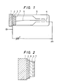
- a typical example of a photoelectric conversion element that can be used in a storage mode occurs in a photoconductive type image pick-up tube, such as that shown in Figure 1 of the accompanying drawings.
- This tube consists of a light-transmitting substrate 1, generally called a "face plate", a transparent conductive film 2, a photoconductive layer 3, an electron gun 4 and a jacket 5.
- An optical image formed on the surface of the photoconductive layer 3 through the face plate 1 is subjected to photoelectric conversion, is stored in the form of charge patterns on the surface of the photoconductive layer and is read sequentially by a scanning electron beam 6.
- a beam impingement layer 7 is formed on the surface of the photoconductive layer 3, in order to prevent the inversion and the injection of electrons from the scanning electron beam.
- One of the significant characteristics required of the photoconductive layer 3 is that the charge patterns do not decay by diffusion during the time interval in which specific picture elements are scanned by the scanning electron beam 6 (i.e. during the storage time).
- a prior art reference that proposes the use of an amorphous material consisting principally of silicon and containing hydrogen for the photoconductive layer is "Appln. Phys. Lett.”, 35(4), 15 Aug., 1979, p349-351.
- a solid state imager using a photoconductor is disclosed, for example in "INTERNATIONAL ELECTRON DEVICES MEETING", December 1979, pl34-136.
- the photoconductor used in this disclosure is a Se-Ge-As chalcogenide glass.
- the present invention is directed to the solution of the above mentioned problem.
- the photoconductive layer is formed of a photoconductive amorphous material consisting principally of silicon but which also contains hydrogen on a first electrode having a metallic surface film containing at least one of Ta, Cr, W, Nd, Mo, V and Ti. This arrangement provides sufficient bonding strength between the amorphous material and the substrate.
- the metallic film may be either a film of a single substance or a composite film. It may alternatively be a multi-layered film. An alloy of two or more of the above mentioned elements may be used.
- this metallic film may itself form the ordinary electrode.
- the film thickness is generally in the range from 2000 ⁇ to 1 ⁇ m. If this film is simultaneously used as a transparent electrode in a multi-layered construction, it is of course necessary that the film used for adhesive purposes is also substantially transparent or semi-transparent. Generally, a thickness of from 5 ⁇ to 100A is preferred. If there is an Al electrode or the like below the film, the film for adhesion may be disposed on the Al electrode. If the metallic film is disposed where electrical conduction is not required, the film thickness is preferably as thin as 20 ⁇ to 200 ⁇ and more preferably is from 50A to 100 ⁇ . It is also advisable to employ a method which suitably divides the conductor so as to interrupt its conductivity.
- the metallic film may be formed by an ordinary sputtering method, for which the conditions are generally as follows. It may be either RF sputtering or DC sputtering.
- the atmosphere used comprises a dilute gas, such as argon at from 5 x 10⁻⁴ to 1 x 10 -2 Torr while an input power of about 200 to about 800W may be used.
- the metallic film may alternatively be formed by the ordinary vacuum evaporation method.
- the photoconductive film in accordance with the present invention consists of a single layer or a laminate layer.
- an amorphous material containing silicon and hydrogen in such amounts that the single layer or at least one layer of the laminate layer, of photoconductive substance contains at least 50 atom% silicon and 5 to 50 atom% hydrogen, and at the same time has a resistivity of at least 10 10 Ohm.cm.
- a-material in which from 0.1% to 50% of the silicon atoms are substituted by germanium atoms.
- the thickness of the photoconductive film is in the range of from 100 nm to 20 ⁇ m.
- the amorphous material can be produced for example by an ordinary reactive sputtering method or with- an ordinary decomposition method by means of a glow discharge.
- a transparent electrode 2 consisting of Sn0 2 was formed on a glass substrate 1 and was fitted to a substrate holder electrode inside a high frequency sputtering device.
- a Ta target was mounted onto a target electrode.
- Ar gas was introduced into -2 the chamber so as to attain a gas pressure of 1.0 x 10 Torr.
- a 99.999% silicon sintered body was mounted on the target electrode and reactive sputtering of the amorphous silicon film 3 was effected onto the Ta film 8 in an atmosphere consisting of 3 x 10⁻³ Torr of Ar and 2 x 10- 3 Torr of H2.
- the substrate was held at 200°C.
- the amorphous silicon film thus produced had about 10 atom% hydrogen and a resistivity of 10 14 Oh m.cm.
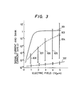
- Figure 3 shows the current-voltage characteristics of an amorphous silicon vidicon target.
- the photocurrent was measured using 10-lux illumination (blue light) on the face plate.
- Curves 101 and 102 represent the signal current and dark current respectively as measured for the target embodying the present invention (the units are arbitrary).
- the curve 103 represents the signal current when the present invention was not used and lines 104 to 108 represent the dark current in each electric field when the present invention was not used. The signal levels in these cases are inferior to those obtained with the present invention, and the difference is further observed very clearly with respect to the dark current characteristics. If film peeling occurs, the target exhibits an extremely large dark current as shown in Figure 3 so that it can not be used in practice.
- a plurality of transparent electrodes consisting of Sn02-In203 were formed on glass substrates and the metallic films shown in Table 1 were formed thereon by sputter evaporation as in Example 1. Then, a silicon layer containing 15 atom% of hydrogen was formed to a thickness of 2 ⁇ m by the reactive sputtering method. Finally, an Sb 2 S 3 film was vacuum evaporated under Ar gas, thereby providing a target for an image pick-up tube. Each target exhibited excellent characteristics in the same way as in the target of Example 1.
- This embodiment relates to a solid state imager using a photoconductive layer.
- This solid state imager has a construction in which a plurality of solid elements each having a photoelectric conversion function and a signal storage function are so arranged that each solid element corresponds to one picture element so as to form an image surface, and the resulting image surfaces are sequentially scanned so as to convert external picture information into electric signals.
- An example of a solid state imager in which the photoconductive layer forming the image surface covers a semiconductor substrate having formed thereon a switch, a scanning circuit and the like, is disclosed in Japanese Laid Open Patent No. 10715/1976.
- FIG. 4 shows the principle of the solid state imager.
- the picture elements 14 are arranged in a matrix and are read out one by one by an XY address system. Selection of the picture elements is made by means of a horizontal scanning signal generator 11 and a vertical scanning signal generator 12. Switch portions 13 are connected to the picture elements and to output terminals 5.
- FIGS 5 to 7 are sectional views of the picture element portions showing a method of production of a solid state imager embodying the present invention.
- the switching circuit formed on the semiconductor substrate, the scanning circuit portions and the like were produced in accordance with the ordinary fabrication methods used for semiconductor devices.
- An SiO 2 film as thin as about 800A was formed on a P-type silicon substrate 20 and an approximately 1400 ⁇ -thick Si 3 N 4 film was then formed at a predetermined position on this Si0 2 film.
- the Si0 2 film was formed by the ordinary CVD process while the Si 2 N 3 film was formed by the CVD process in the presence of Si3N4, NH 4 and N 2 .
- a p- type diffusion region 21 was formed from the upper portion of the silicon substrate by ion implantation. This diffusion region was formed in order to improve separation of the picture elements.
- This process is a local oxidation process for silicon that is generally referred to as an "LOCOS".
- the above mentioned Si 3 N 4 and SiO 2 film were then removed and a gate insulation film of an MOS transistor was formed by the Si0 2 film.
- a gate portion 25 of poly-silicon and diffusion regions 26,27 were formed and an Si0 2 film 28 was formed on them.
- electrode extension portions of source 26 and drain 27 by etching As a drain electrode 29, Al was vacuum evaporated to a thickness of 8000 ⁇ .
- a Si0 2 film 30 was then formed to a thickness of 7500 ⁇ , followed by vacuum deposition of l ⁇ m thick Al as the source electrode 31.
- a Ta layer 32 was then sputter evaporated to a thickness of 100 ⁇ .
- Figure 6 is a sectional view showing this state. Incidentally, the electrode 31 was formed so as to cover the regions 26,27 and the gate portion. This arrangement was employed because if the light enters the signal processing region between the diffusion layers 21 separating the elements, it causes undesirable blooming.
- FIG. 8 is a plan view of the Si substrate portion, showing an electrode contact hole 37.
- the same reference numerals as used in the sectional view represent the same constituents.
- an amorphous silicon layer 33 containing 15 atom% of hydrogen was formed to a thickness of 2 ⁇ m by the reactive sputtering process.
- a transparent electrode 35 was formed on this layer 33, thereby completing the solid state imager.
- the transparent electrode it is possible to use a ultrathin film of gold or the like or a transparent electroconductive film containing indium oxide or tin oxide, or a ribbon like metallic film.
- a conductive film 36 forming an ohmic contact was disposed on the other surface of the semiconductor substrate 20. Generally, this conductive film 36 is grounded through a terminal.
- Cr-Au was vacuum evaporated onto a part of the transparent electrode using a mask, and wire-bonding was effected at this portion so as to form a biasing electrode.
- the solid state imager using the amorphous silicon as the photoconductive film was completed.
- the Ta layer 32 was disposed at the upper portion of the substrate on which the amorphous silicon film 33 was to be formed, peeling of the amorphous silicon film could be completely eliminated.
- FIG. 5 to 7 is one in which the metal layer serving as the adhesive layer is laminated on the metal layer forming the electrode.
- the electrode 31 per se may consist of a metal which is to serve as the adhesive layer.
- the construction of the electrode portion is of course not specifically restricted to that used in this embodiment.
- Figure 9 shows an example in which the present invention was applied to an electrode having a two-layered construction. Its fundamental construction is the same as in the foregoing examples. It.has an impurity layer 45 in the silicon substrate 20 and an insulation film 22 for separating the picture elements consisting of Si0 2 or the like. An insulation film 28 consisting of Si0 2 or P-containing Si0 2 ..
- a lower electrode 29 consisting of Al was disposed on the insulation film 28 and an upper electrode 40 was further formed thereon via the insulation film 30.
- the metallic film 41 of the present invention was formed of Ta on the upper electrode 40.
- the photoconductive film 32 and the transparent electrode 35 were sequentially formed, thereby providing the solid state image pick up element.
- the scanning circuit in this example consisted of MOS field effect transistors
- the present invention is not restricted to this construction. It is of course possible to use a CCD (Charge Coupled Device) transfer region as the scanning circuit, for example. It is further possible to use MOS transistors or other circuit systems.
- CCD Charge Coupled Device
- the present invention can be adapted to photoelectric conversion devices of various modified constructions using the above mentioned amorphous material consisting of silicon as the principal component and containing hydrogen, and also using a rectification contact type construction.
- the present invention provides an improved construction of light-receiving surface which can sufficiently restrict the dark current even when a strong electric field is applied to the interface of junction.
- a film layer consisting principally of at least one of the oxides, nitrides and halides selected from the group listed below may be interposed between the photoconductive layer consisting of H-containing amorphous material and a signal electrode.
- Particular examples includes SiO 2 , Ti0 2 , Al 2 O 3 , M g O, BaO, Ta205, W03, Bi 2 0 3 , V 2 O 5 , GeO, NiO, Th 0 2 , Fe 2 O 3 , La 2 O 3 , MoO 3 , BeO, Sc 2 0 3 , Co 2 O 3 and their eutectic mixtures.
- Particular examples include GaN, Si 3 N 4 , Si 2 N 3 , MgN 2 , TaN, HfN, ZrN, NbN, BN and their eutectic mixtures.
- Particular examples include MgF 2 , LiF, NaF, BaF 2 , CaF 2 , KF and their eutectic mixtures.
- SiO 2 , BaO, Ti0 2 , Ta 2 O 5 or Al203 as the oxide, Si 3 N 4 or TaN as the nitride and LiF or MgF 2 as the halide can exhibit extremely good characteristics, followed by M g O, WO 3 , V 2 O 5 , NiO, Fe 2 O 3 , MoO 3 or Co 2 O 3 as the oxide, G aN, Si 2 N 3 or MgN 2 as the nitride and BaF 2 , NaF and KF as the halide. Good characteristics can also be obtained from Bi 2 0 3 , GeO, Th0 2 , La 2 O 3 , Be0 or Sc0 3 as the oxide and HfN, ZnN, NbN or BN as the nitride.
- the film thickness ranges from about 50 ⁇ to about 5000A. Especially when the film thickness is below 1000A, there are no problems such as a decrease in the transmissivity of the incident light or reduction of the sensitivity of the photoelectric conversion device.
- the above mentioned oxide layer be formed by the sputtering vacuum deposition process using the same oxide as the material for vacuum deposition.
- the sputtering vacuum deposition generally uses a high frequency discharge in Ar gas at 1 x 10 -1 Torr to 1 x 10 -3 Torr. If the oxide is likely to be reduced and to become blackened in this instance, it is advisable to blend up to about 5% by volume of oxygen with the Ar gas.
- the temperature of the substrate during vacuum evaporation may be 25 to 400°C, it is preferably from 100 to 250°C in order to prepare a flat film.
- the film layer consisting of the abovementioned oxide, nitride or halide is interposed between the photoconductive film and the signal electrode, but it is not always necessary for the film to be disposed adjacent to the signal electrode. In other words, a layer consisting of other materials may be interposed between the signal electrode and the film layer. However, it is necessary that the photoconductive film and the oxide be substantially adjacent to each other.
- Figure 10 is a sectional view of a target of the invention of this type.
- Reference numeral 42 represents the above mentioned film layer for restricting the dark current.
- the other constituents are the same as those of Figure 7 and are represented by the same reference numerals.
- the thin film layers shown in the following Tables 2 and 3 were employed as the layer 42, respectively, but peeling of the conductive film did not occur at all and the dark current could be restricted to a sufficiently low level even at a high target voltage. Details of the formation of the layers 42 by sputtering are given in Table 2, and the method of formation is indicated in Table 3.
Landscapes
- Physics & Mathematics (AREA)
- Electromagnetism (AREA)
- Engineering & Computer Science (AREA)
- Power Engineering (AREA)
- Condensed Matter Physics & Semiconductors (AREA)
- General Physics & Mathematics (AREA)
- Computer Hardware Design (AREA)
- Microelectronics & Electronic Packaging (AREA)
- Solid State Image Pick-Up Elements (AREA)
- Light Receiving Elements (AREA)
- Transforming Light Signals Into Electric Signals (AREA)
- Image-Pickup Tubes, Image-Amplification Tubes, And Storage Tubes (AREA)
Applications Claiming Priority (2)
| Application Number | Priority Date | Filing Date | Title |
|---|---|---|---|
| JP462280A JPS56103477A (en) | 1980-01-21 | 1980-01-21 | Photoelectric conversion element |
| JP4622/80 | 1980-01-21 |
Publications (3)
| Publication Number | Publication Date |
|---|---|
| EP0032847A2 true EP0032847A2 (fr) | 1981-07-29 |
| EP0032847A3 EP0032847A3 (en) | 1982-04-28 |
| EP0032847B1 EP0032847B1 (fr) | 1985-05-08 |
Family
ID=11589145
Family Applications (1)
| Application Number | Title | Priority Date | Filing Date |
|---|---|---|---|
| EP81300269A Expired EP0032847B1 (fr) | 1980-01-21 | 1981-01-21 | Elément de conversion photoélectrique et dispositif de prise de vue |
Country Status (5)
| Country | Link |
|---|---|
| US (1) | US4554478A (fr) |
| EP (1) | EP0032847B1 (fr) |
| JP (1) | JPS56103477A (fr) |
| CA (1) | CA1154133A (fr) |
| DE (1) | DE3170357D1 (fr) |
Cited By (8)
| Publication number | Priority date | Publication date | Assignee | Title |
|---|---|---|---|---|
| EP0031663A2 (fr) * | 1979-12-14 | 1981-07-08 | Hitachi, Ltd. | Dispositif photoélectrique |
| EP0053946A2 (fr) * | 1980-12-10 | 1982-06-16 | Fuji Xerox Co., Ltd. | Matrice linéaire de lecture en film mince |
| EP0111899A2 (fr) * | 1982-12-16 | 1984-06-27 | Hitachi, Ltd. | Dispositif semi-conducteur et procédé pour sa fabrication |
| GB2150785A (en) * | 1983-11-24 | 1985-07-03 | Sharp Kk | Two-dimensional image read-out device |
| EP0204554A2 (fr) * | 1985-06-04 | 1986-12-10 | Siemens Solar Industries L.P. | Dispositif photoconducteur comportant une couche conductrice transparente d'oxyde de zinc |
| FR2585183A1 (fr) * | 1985-07-19 | 1987-01-23 | Thomson Csf | Procede de fabrication d'un detecteur d'image lumineuse et detecteur matriciel bidimensionnel obtenu par ce procede |
| EP0251647A2 (fr) * | 1986-06-27 | 1988-01-07 | Hitachi, Ltd. | Cible pour tube de prise de vues |
| US5078803A (en) * | 1989-09-22 | 1992-01-07 | Siemens Solar Industries L.P. | Solar cells incorporating transparent electrodes comprising hazy zinc oxide |
Families Citing this family (7)
| Publication number | Priority date | Publication date | Assignee | Title |
|---|---|---|---|---|
| JPS5863164A (ja) * | 1981-10-13 | 1983-04-14 | Fuji Xerox Co Ltd | 光読取り素子 |
| JPS5882564A (ja) * | 1981-11-12 | 1983-05-18 | Fuji Xerox Co Ltd | 非晶質シリコン受光素子 |
| JPS59229860A (ja) * | 1983-05-23 | 1984-12-24 | Fuji Xerox Co Ltd | 光電変換素子およびその製造方法 |
| JPS6035550U (ja) * | 1983-08-18 | 1985-03-11 | 東北リコ−株式会社 | アモルフアスシリコンラインセンサ |
| EP0215289B1 (fr) * | 1985-08-23 | 1991-10-09 | Siemens Aktiengesellschaft | Procédé de fabrication d'une structure de diode de blocage en a-Si:H pour senseurs linéaires d'images |
| US5973259A (en) * | 1997-05-12 | 1999-10-26 | Borealis Tech Ltd | Method and apparatus for photoelectric generation of electricity |
| ITMI20111559A1 (it) * | 2011-08-30 | 2013-03-01 | St Microelectronics Srl | Strato tco di contatto frontale di un pannello solare a film sottile con strato barriera di metallo refrattario e processo di fabbricazione |
Citations (4)
| Publication number | Priority date | Publication date | Assignee | Title |
|---|---|---|---|---|
| JPS5195720A (fr) * | 1975-02-19 | 1976-08-21 | ||
| US4167015A (en) * | 1978-04-24 | 1979-09-04 | Rca Corporation | Cermet layer for amorphous silicon solar cells |
| EP0025872A2 (fr) * | 1979-09-21 | 1981-04-01 | Messerschmitt-Bölkow-Blohm Gesellschaft mit beschränkter Haftung | Composant semiconducteur servant à la conversion de rayonnement solaire en énergie électrique |
| EP0031663A2 (fr) * | 1979-12-14 | 1981-07-08 | Hitachi, Ltd. | Dispositif photoélectrique |
Family Cites Families (7)
| Publication number | Priority date | Publication date | Assignee | Title |
|---|---|---|---|---|
| US3350595A (en) * | 1965-11-15 | 1967-10-31 | Rca Corp | Low dark current photoconductive device |
| JPS5240809B2 (fr) * | 1972-04-07 | 1977-10-14 | ||
| JPS5926154B2 (ja) * | 1974-07-05 | 1984-06-25 | 株式会社日立製作所 | 固体撮像装置 |
| JPS54139342A (en) * | 1978-04-20 | 1979-10-29 | Canon Inc | Information processing unit |
| JPS54150995A (en) * | 1978-05-19 | 1979-11-27 | Hitachi Ltd | Photo detector |
| JPS561318A (en) * | 1979-06-18 | 1981-01-09 | Canon Inc | Photoelectric conversion device |
| JPS5630373A (en) * | 1979-08-20 | 1981-03-26 | Matsushita Electric Ind Co Ltd | Solid image pickup unit |
-
1980
- 1980-01-21 JP JP462280A patent/JPS56103477A/ja active Granted
-
1981
- 1981-01-21 CA CA000368960A patent/CA1154133A/fr not_active Expired
- 1981-01-21 DE DE8181300269T patent/DE3170357D1/de not_active Expired
- 1981-01-21 EP EP81300269A patent/EP0032847B1/fr not_active Expired
-
1983
- 1983-05-25 US US06/497,841 patent/US4554478A/en not_active Expired - Lifetime
Patent Citations (4)
| Publication number | Priority date | Publication date | Assignee | Title |
|---|---|---|---|---|
| JPS5195720A (fr) * | 1975-02-19 | 1976-08-21 | ||
| US4167015A (en) * | 1978-04-24 | 1979-09-04 | Rca Corporation | Cermet layer for amorphous silicon solar cells |
| EP0025872A2 (fr) * | 1979-09-21 | 1981-04-01 | Messerschmitt-Bölkow-Blohm Gesellschaft mit beschränkter Haftung | Composant semiconducteur servant à la conversion de rayonnement solaire en énergie électrique |
| EP0031663A2 (fr) * | 1979-12-14 | 1981-07-08 | Hitachi, Ltd. | Dispositif photoélectrique |
Non-Patent Citations (1)
| Title |
|---|
| THE CONFERENCE OF THE TWELFTH IEEE PHOTOVOLTAIC SPECIALISTS CONFERENCE 1976, 15th-18th November 1976, pages 893-895 Baton Rouge, Louisiana, U.S.A. D.E. CARLSON et al.: "Solar cells using Schottky barriers on amorphous silicon" * |
Cited By (14)
| Publication number | Priority date | Publication date | Assignee | Title |
|---|---|---|---|---|
| EP0031663A3 (en) * | 1979-12-14 | 1982-04-21 | Hitachi, Ltd. | Photoelectric device |
| EP0031663A2 (fr) * | 1979-12-14 | 1981-07-08 | Hitachi, Ltd. | Dispositif photoélectrique |
| EP0053946A2 (fr) * | 1980-12-10 | 1982-06-16 | Fuji Xerox Co., Ltd. | Matrice linéaire de lecture en film mince |
| EP0053946A3 (en) * | 1980-12-10 | 1984-07-11 | Fuji Xerox Co., Ltd. | Elongate thin-film reader |
| EP0111899A3 (en) * | 1982-12-16 | 1987-01-28 | Hitachi, Ltd. | Semiconductor device and method of manufacturing the same |
| EP0111899A2 (fr) * | 1982-12-16 | 1984-06-27 | Hitachi, Ltd. | Dispositif semi-conducteur et procédé pour sa fabrication |
| GB2150785A (en) * | 1983-11-24 | 1985-07-03 | Sharp Kk | Two-dimensional image read-out device |
| EP0204554A2 (fr) * | 1985-06-04 | 1986-12-10 | Siemens Solar Industries L.P. | Dispositif photoconducteur comportant une couche conductrice transparente d'oxyde de zinc |
| EP0204554A3 (fr) * | 1985-06-04 | 1987-04-08 | Siemens Solar Industries L.P. | Dispositif photoconducteur comportant une couche conductrice transparente d'oxyde de zinc |
| FR2585183A1 (fr) * | 1985-07-19 | 1987-01-23 | Thomson Csf | Procede de fabrication d'un detecteur d'image lumineuse et detecteur matriciel bidimensionnel obtenu par ce procede |
| EP0211720A1 (fr) * | 1985-07-19 | 1987-02-25 | Thomson-Csf | Procédé de fabrication d'un détecteur d'image lumineuse, et détecteur matriciel bidimensionnel obtenu par ce procédé |
| EP0251647A2 (fr) * | 1986-06-27 | 1988-01-07 | Hitachi, Ltd. | Cible pour tube de prise de vues |
| EP0251647A3 (en) * | 1986-06-27 | 1989-10-18 | Hitachi, Ltd. | Target of image pickup tube |
| US5078803A (en) * | 1989-09-22 | 1992-01-07 | Siemens Solar Industries L.P. | Solar cells incorporating transparent electrodes comprising hazy zinc oxide |
Also Published As
| Publication number | Publication date |
|---|---|
| EP0032847A3 (en) | 1982-04-28 |
| EP0032847B1 (fr) | 1985-05-08 |
| US4554478A (en) | 1985-11-19 |
| JPH0159744B2 (fr) | 1989-12-19 |
| CA1154133A (fr) | 1983-09-20 |
| DE3170357D1 (en) | 1985-06-13 |
| JPS56103477A (en) | 1981-08-18 |
Similar Documents
| Publication | Publication Date | Title |
|---|---|---|
| EP0032847B1 (fr) | Elément de conversion photoélectrique et dispositif de prise de vue | |
| US4360821A (en) | Solid-state imaging device | |
| EP0039219B1 (fr) | Ecran photosensible et dispositifs contenant un tel écran | |
| EP0005543B1 (fr) | Capteur photosensible | |
| US4665609A (en) | Process of manufacturing a photosensitive device having a plurality of detectors separated by zones impervious to the radiation to be detected | |
| EP0060699B1 (fr) | Procédé de fabrication de capteurs photosensibles | |
| US4687922A (en) | Image detector operable in day or night modes | |
| EP0029679B1 (fr) | Dispositif photoélectrique | |
| CA1161534A (fr) | Convertisseur photoelectrique | |
| JPS63244879A (ja) | 固体撮像装置 | |
| EP0031663B1 (fr) | Dispositif photoélectrique | |
| CA1145835A (fr) | Dispositif photoelectrique, et methode de production connexe | |
| US5399882A (en) | Camera device and method of manufacturing the same | |
| KR840002185B1 (ko) | 광전변환소자 | |
| EP0045203A2 (fr) | Procédé pour la fabrication d'un dispositif de prise de vues | |
| KR850001099B1 (ko) | 수광면(受光面) | |
| JPH0214790B2 (fr) | ||
| KR840001163B1 (ko) | 광전변환 장치 | |
| US4883562A (en) | Method of making a photosensor | |
| JPS6244696B2 (fr) | ||
| JPH0810582B2 (ja) | 受光素子 | |
| KR900000350B1 (ko) | 광전 변환 장치 | |
| JPH04211171A (ja) | 受光素子 | |
| JPH03129770A (ja) | 固体撮像装置 | |
| JPH04112434A (ja) | 撮像管およびその動作方法 |
Legal Events
| Date | Code | Title | Description |
|---|---|---|---|
| PUAI | Public reference made under article 153(3) epc to a published international application that has entered the european phase |
Free format text: ORIGINAL CODE: 0009012 |
|
| 17P | Request for examination filed |
Effective date: 19810422 |
|
| AK | Designated contracting states |
Designated state(s): DE FR GB NL |
|
| RBV | Designated contracting states (corrected) |
Designated state(s): DE FR GB NL |
|
| PUAL | Search report despatched |
Free format text: ORIGINAL CODE: 0009013 |
|
| AK | Designated contracting states |
Designated state(s): DE FR GB NL |
|
| GRAA | (expected) grant |
Free format text: ORIGINAL CODE: 0009210 |
|
| AK | Designated contracting states |
Designated state(s): DE FR GB NL |
|
| REF | Corresponds to: |
Ref document number: 3170357 Country of ref document: DE Date of ref document: 19850613 |
|
| ET | Fr: translation filed | ||
| PLBE | No opposition filed within time limit |
Free format text: ORIGINAL CODE: 0009261 |
|
| STAA | Information on the status of an ep patent application or granted ep patent |
Free format text: STATUS: NO OPPOSITION FILED WITHIN TIME LIMIT |
|
| 26N | No opposition filed | ||
| PGFP | Annual fee paid to national office [announced via postgrant information from national office to epo] |
Ref country code: FR Payment date: 19940120 Year of fee payment: 14 |
|
| PGFP | Annual fee paid to national office [announced via postgrant information from national office to epo] |
Ref country code: NL Payment date: 19940131 Year of fee payment: 14 |
|
| PGFP | Annual fee paid to national office [announced via postgrant information from national office to epo] |
Ref country code: DE Payment date: 19940328 Year of fee payment: 14 |
|
| PGFP | Annual fee paid to national office [announced via postgrant information from national office to epo] |
Ref country code: GB Payment date: 19950104 Year of fee payment: 15 |
|
| PG25 | Lapsed in a contracting state [announced via postgrant information from national office to epo] |
Ref country code: NL Effective date: 19950801 |
|
| PG25 | Lapsed in a contracting state [announced via postgrant information from national office to epo] |
Ref country code: FR Effective date: 19950929 |
|
| NLV4 | Nl: lapsed or anulled due to non-payment of the annual fee |
Effective date: 19950801 |
|
| PG25 | Lapsed in a contracting state [announced via postgrant information from national office to epo] |
Ref country code: DE Effective date: 19951003 |
|
| REG | Reference to a national code |
Ref country code: FR Ref legal event code: ST |
|
| PG25 | Lapsed in a contracting state [announced via postgrant information from national office to epo] |
Ref country code: GB Effective date: 19960121 |
|
| GBPC | Gb: european patent ceased through non-payment of renewal fee |
Effective date: 19960121 |