EP0029631B1 - Mémoire électronique de sécurité utilisable en signalisation ferroviaire - Google Patents
Mémoire électronique de sécurité utilisable en signalisation ferroviaire Download PDFInfo
- Publication number
- EP0029631B1 EP0029631B1 EP80201096A EP80201096A EP0029631B1 EP 0029631 B1 EP0029631 B1 EP 0029631B1 EP 80201096 A EP80201096 A EP 80201096A EP 80201096 A EP80201096 A EP 80201096A EP 0029631 B1 EP0029631 B1 EP 0029631B1
- Authority
- EP
- European Patent Office
- Prior art keywords
- voltage
- oscillator
- memory
- transistor
- input
- Prior art date
- Legal status (The legal status is an assumption and is not a legal conclusion. Google has not performed a legal analysis and makes no representation as to the accuracy of the status listed.)
- Expired
Links
- 230000015654 memory Effects 0.000 title claims description 44
- 230000011664 signaling Effects 0.000 title claims description 3
- 238000004804 winding Methods 0.000 claims description 31
- 239000003990 capacitor Substances 0.000 claims description 21
- 230000008034 disappearance Effects 0.000 claims description 14
- 230000006870 function Effects 0.000 claims description 14
- 230000010355 oscillation Effects 0.000 claims description 11
- 230000007704 transition Effects 0.000 claims description 9
- 239000013642 negative control Substances 0.000 claims description 2
- 230000000903 blocking effect Effects 0.000 claims 1
- 230000002459 sustained effect Effects 0.000 claims 1
- 239000004020 conductor Substances 0.000 description 7
- 238000010586 diagram Methods 0.000 description 5
- 230000009471 action Effects 0.000 description 3
- 230000008859 change Effects 0.000 description 3
- 230000000295 complement effect Effects 0.000 description 3
- 239000013641 positive control Substances 0.000 description 3
- 230000010287 polarization Effects 0.000 description 2
- 230000001052 transient effect Effects 0.000 description 2
- 238000011144 upstream manufacturing Methods 0.000 description 2
- 230000007547 defect Effects 0.000 description 1
- 230000000694 effects Effects 0.000 description 1
- 230000001939 inductive effect Effects 0.000 description 1
- 238000002955 isolation Methods 0.000 description 1
- 238000012423 maintenance Methods 0.000 description 1
- 230000008685 targeting Effects 0.000 description 1
- 230000003797 telogen phase Effects 0.000 description 1
- 230000003313 weakening effect Effects 0.000 description 1
Images
Classifications
-
- B—PERFORMING OPERATIONS; TRANSPORTING
- B61—RAILWAYS
- B61L—GUIDING RAILWAY TRAFFIC; ENSURING THE SAFETY OF RAILWAY TRAFFIC
- B61L1/00—Devices along the route controlled by interaction with the vehicle or train
- B61L1/20—Safety arrangements for preventing or indicating malfunction of the device, e.g. by leakage current, by lightning
-
- G—PHYSICS
- G11—INFORMATION STORAGE
- G11C—STATIC STORES
- G11C11/00—Digital stores characterised by the use of particular electric or magnetic storage elements; Storage elements therefor
- G11C11/19—Digital stores characterised by the use of particular electric or magnetic storage elements; Storage elements therefor using non-linear reactive devices in resonant circuits
- G11C11/20—Digital stores characterised by the use of particular electric or magnetic storage elements; Storage elements therefor using non-linear reactive devices in resonant circuits using parametrons
Definitions
- the invention relates to an electronic safety memory comprising on the one hand a first DC supply voltage input, a second control input and an output, on the other hand a transistor oscillator including a primary transformer winding connected to the collector. reacts via said transformer on a first secondary winding connected to another electrode of said transistor so as to create a feedback loop to generate the oscillation, the frequency of which is determined by a first capacitor connected in parallel to said primary winding, said memory being reset to zero by cutting off the supply voltage.
- Such a safety memory finds its main application in the field of railway signaling. It can in particular be used in a processing box where it is part of a logic unit aiming at the control of a user relay which commands for example the closing of a level crossing, from signals emitted by the sensors of an electronic pedal when passing a train.
- the supply voltage input is used to validate the memory, that is to say that in the absence of the DC supply voltage, the output state is necessarily "0 •, this state can be” 1 or "0 when the supply voltage is present.
- the control input receives a signal which is either a direct voltage or a zero voltage, this control signal carrying the information to be memorized.
- such a memory operates in sequence, its output state being able to be different for certain states of identical inputs as a function of the previous states of the inputs and their transitions.
- the memory according to French patent 1 281 318 is positive control, that is to say that it memorizes the appearance of the DC voltage of the control signal, by delivering an output signal equal to "1 during this appearance, state “1” self-maintaining later whatever the waveform of the control signal between its two possible states defined above.
- the memory is then reset to zero by cutting off the supply voltage on the first input.
- the logical sequence to be carried out is indicated in table 1 on page 3 of the aforementioned patent.
- the memory of the prior art described above is applicable when the control signal is zero at rest and that it becomes non-zero when an external event occurs. In some cases, however, it is more interesting that the appearance of this external event is accompanied by the weakening or disappearance of a normally present signal.
- a negative oriented pedal works, for example, which has two electronic sensors arranged fairly close together on a railway track. These sensors are, at rest, permanently supplied with alternating current, each at a predetermined frequency, by an oscillator, which goes in the direction of safety. This alternating signal, the amplitude of which exceeds a certain threshold, is reflected at the level of a processing box, for each sensor, by a DC voltage signal. The output signal from the processing box itself controls a relay. When a rail vehicle axle passes in front of each sensor, an inductive variation is created in the latter, which has the effect of lowering the amplitude of the AC signal, below the aforementioned threshold, which, in the processing box , results in the zero crossing of said DC voltage signal.
- the invention proposes to solve the aforementioned drawbacks of the prior art.
- the electronic security memory defined in the preamble is remarkable in that, according to the invention, it is negatively controlled and that for this purpose it includes the characteristics of the characterizing part of claim 1.
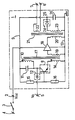
- the single figure is an electronic diagram of a safety memory according to the invention, using a transistor oscillator mounted as a common emitter.
- the memory 1 of the figure comprises a first supply voltage input connected to the input terminal 2. This terminal is connected via a switch 3 to a terminal 4 which permanently receives a direct voltage from power supply V dc , except accidental cut, upstream, of this tension.
- the switch 3 is for example controlled by a relay, not shown, this relay can be the user relay controlled by the output of a processing box, not shown, of which memory 1 is a part.
- a second control input is connected to input terminal 5.
- An output connected between terminals 6 and 7 delivers a signal which can either be an AC voltage signal, which constitutes the logic value "1 or a zero voltage signal, which constitutes the value logic "0 •.
- the essential part of the memory is constituted by an oscillator comprising a transistor 8, the collector of which is connected to a conductor 9, by means of the parallel mounting of a choke 10 and of a capacitor 11.
- the collector is also connected to terminal 5 via a diode 12 mounted in reverse.
- the emitter of the transistor 8 is connected to the ground conductor 13 via an inductor 14.
- the base of the transistor is connected to the conductor 9 via the resistor 15 and to ground via the resistor 16, these two resistors serving for its polarization.
- the inductor 10 constitutes the primary winding of a transformer 17, a secondary winding of which consists of the inductor 14.
- the assembly comprising the elements 9 to 11 and 13 to 17 , apart from input 5 and diode 12, constitutes a transistor oscillator, with parallel-series reaction, the transistor being mounted as a common emitter.
- the windings 10 and 14 must be in the same direction and that the number of turns of the primary winding 10 is of the order of 10 times greater to that of the secondary winding 14.
- the oscillation frequency is determined by the values L 10 and C 11 of the inductance and the capacitance of the elements 10 and 11 respectively. Such an oscillator works correctly for a frequency range preferably between 1 and 10 kHz.
- the safety memory includes an amplifier 18 which is supplied between terminal 2 and ground. Its input is connected to ground via an inductor 19 which constitutes a second secondary winding of the transformer 17. Its output delivers, when the oscillator is operating, a square signal at the frequency of oscillation in a primary winding 20 a second transformer 21, the winding 20 being connected to ground by its other end.
- the transformer 21 has two secondaries which are the winding 22 whose ends are connected to the output terminals 6 and 7 and the winding 23 whose one end is connected to the ground and the other to an electrode (for example the anode ) a diode 24.
- the other electrode of the diode 24 is connected to the connection point 25 which belongs to the conductor 9 and which is connected, via a capacitor 26, to ground.
- the assembly constituted by the diode 24 and the capacitor 26 is used for rectifying the alternating current whose winding 23 is the seat when the oscillator is operating. Thanks to the energy supply due to the amplifier 18, the entire device is able to maintain itself in an oscillation state by compensating for its losses, the capacitor 26 then acting as a battery. In order not to disturb this voltage rectification circuit, and to obtain galvanic isolation, the output of the device is taken on the separate secondary winding, 22, of the transformer 21.
- the amplifier 18 being supplied, that is to say the switch 3 being closed, the oscillator remains blocked as long as the voltage across the terminals of the capacitor 25 remains close to zero and it cannot unblock itself.
- a positive voltage of a few volts at point 25 is enough to start it up, even if this positive voltage is less than the supply voltage V cc .
- Vdc supply voltage
- the voltage on the input terminal 5 can take the value for example positive V c such that: V c ⁇ V cc , or the zero value, values with which the logical values "1" and "0" are associated by convention respectively for facilitate reasoning.
- the logic for example positive V cc and the zero voltage on the power input terminal 2, are made to correspond to the logic states "1 and" 0 respectively.
- the memory Since the memory operates in sequence, we start for example from a rest phase called the first zeroing phase for which the inputs 2 and 5 are both in the logic state “0 It then delivers a logic state at its output” 0 the amplifier 18 is not supplied. The memory is then armed by passing the input 2 to the state “1 e 5 being always in the state“ 0 •, that is to say by closing the switch 3. In this second phase of arming the memory always delivers a “0 since the capacitor 26 is not charged. Then we pass to a third phase by passing the entry 5 from "0 to" 1 ".
- the capacitor 26 is almost charged at the voltage V c via the diode 12 in the passing direction, the winding 10 and the conductor 9 (except for the voltage drop across the diode 12, which is negligible).
- the oscillator always remains blocked (zero voltage at the output of the memory) because although the capacitor 26 is charged at a correct voltage to generate the oscillation, the latter cannot start, the collector of the transistor 8 being biased at a voltage too low relative to its base (after a transient state the potentials of the collector and of the conductor 9 are substantially equal).
- the transition to a fourth phase consists, starting from the third phase, in suppressing the control voltage V c , which results in unblocking the oscillator which starts its oscillation from the voltage V c of the capacitor 26 then, while continuing to oscillate increases the voltage of the latter up to the value V cc . If the control voltage is restored on the input terminal 5, which constitutes a fifth phase, this cannot affect the operation of the oscillator since the voltage on the collector of transistor 8 is then greater than the voltage V c by virtue of the inequality V c ⁇ V cc , the respective values of V c and V cc being judiciously chosen, and that the diode 12 is reverse biased during this fifth state. Stopping the oscillator, i.e. resetting the memory to zero, can then only be obtained by cutting the supply voltage (opening of switch 3) whatever the logic state on the input 5.
- table 1 The logic sequence described above which one wishes to obtain in normal memory operation is summarized in table 1 below:
- a person skilled in the art is able to verify that no other sequence exists, by action on the logic input values, which can cause the start-up and the self-maintenance of the oscillator, i.e. memorize something other than a falling edge on the control input 5, provided that the capacitor 26 does not have a timing function, that is to say that its capacity is of low value.
- the capacitor 26 will not be able to charge which will make the oscillator unable to operate. If it is short-circuited the fifth phase described above can no longer be ensured since the return of the voltage V c on the input terminal 5 will cause the oscillator to stop by polarizing its collector at the voltage V c .
- the safety memory it may be necessary to memorize a disappearance of the voltage V c for a very short time before the supply voltage V cc appears.
- the disappearance of the control voltage V c indirectly causes the appearance of the supply voltage V cc , by closing the switch 3 following the fall of a relay.
- a predetermined delay time T of the order of a few tenths of seconds then elapses between the disappearance of the voltage V c on the input terminal 5 and the appearance of the voltage V cc on the input terminal 2
- the capacitor 26 has an increased capacity such that after time T , it is still in a condition to operate the oscillator, that is to say at the instant when the supply voltage V cc appears and allows the oscillation to be maintained.
- Table II summarizes the logical sequence that it is possible to obtain, the sequence given in table 1 above still remaining possible:
- the safety memory according to the invention is with negative supply: the voltages V c and V cc have negative values, V cc have negative values, V cc being larger, in absolute value than V c , the transistor 8 is then a PNP transistor, the electrode connections remaining the same as that indicated for the NPN transistor in the figure and the diodes 12 and 14 are mounted in the opposite direction to the direction indicated in the figure, all other things remaining equal in the diagram of the single figure.
Landscapes
- Engineering & Computer Science (AREA)
- Automation & Control Theory (AREA)
- Mechanical Engineering (AREA)
- Physics & Mathematics (AREA)
- Nonlinear Science (AREA)
- Computer Hardware Design (AREA)
- Train Traffic Observation, Control, And Security (AREA)
- Dc-Dc Converters (AREA)
- Techniques For Improving Reliability Of Storages (AREA)
- Inductance-Capacitance Distribution Constants And Capacitance-Resistance Oscillators (AREA)
Applications Claiming Priority (2)
| Application Number | Priority Date | Filing Date | Title |
|---|---|---|---|
| FR7928720 | 1979-11-21 | ||
| FR7928720A FR2470478A1 (fr) | 1979-11-21 | 1979-11-21 | Memoire electronique de securite utilisable en signalisation ferroviaire |
Publications (2)
| Publication Number | Publication Date |
|---|---|
| EP0029631A1 EP0029631A1 (fr) | 1981-06-03 |
| EP0029631B1 true EP0029631B1 (fr) | 1984-07-04 |
Family
ID=9231950
Family Applications (1)
| Application Number | Title | Priority Date | Filing Date |
|---|---|---|---|
| EP80201096A Expired EP0029631B1 (fr) | 1979-11-21 | 1980-11-20 | Mémoire électronique de sécurité utilisable en signalisation ferroviaire |
Country Status (7)
| Country | Link |
|---|---|
| US (1) | US4376269A (cg-RX-API-DMAC7.html) |
| EP (1) | EP0029631B1 (cg-RX-API-DMAC7.html) |
| JP (1) | JPS5693200A (cg-RX-API-DMAC7.html) |
| AU (1) | AU532027B2 (cg-RX-API-DMAC7.html) |
| CA (1) | CA1175502A (cg-RX-API-DMAC7.html) |
| DE (1) | DE3068461D1 (cg-RX-API-DMAC7.html) |
| FR (1) | FR2470478A1 (cg-RX-API-DMAC7.html) |
Families Citing this family (7)
| Publication number | Priority date | Publication date | Assignee | Title |
|---|---|---|---|---|
| US4755772A (en) * | 1987-06-05 | 1988-07-05 | Avantek, Inc. | Switchable microwave oscillator |
| JPH02113596A (ja) * | 1988-10-21 | 1990-04-25 | Nec Corp | プリント回路基板 |
| JPH03206655A (ja) * | 1990-01-08 | 1991-09-10 | Matsushita Electric Ind Co Ltd | 電子回路基板 |
| JPH05291735A (ja) * | 1992-04-14 | 1993-11-05 | Unisia Jecs Corp | プリント配線基板 |
| AU2003285675A1 (en) * | 2003-01-10 | 2004-08-10 | Koninklijke Philips Electronics N.V. | Circuit arrangement and method for protecting electronic components against illicit manipulation |
| CN112441080B (zh) * | 2019-08-30 | 2022-09-06 | 比亚迪股份有限公司 | 列车定位方法、设备、系统、计算机设备及存储介质 |
| CN114744880B (zh) * | 2022-04-17 | 2025-09-30 | 杭州欧佩捷科技有限公司 | 无额外绕组的zvs正激式变换器 |
Family Cites Families (4)
| Publication number | Priority date | Publication date | Assignee | Title |
|---|---|---|---|---|
| FR1171567A (fr) * | 1957-02-04 | 1959-01-28 | Signaleur électronique | |
| BE572303A (cg-RX-API-DMAC7.html) * | 1957-11-15 | |||
| FR1281318A (fr) * | 1960-11-28 | 1962-01-12 | Westinghouse Freins & Signaux | Mémoire électronique de sécurité susceptible d'être temporisée |
| FR1405259A (fr) * | 1964-05-11 | 1965-07-09 | Westinghouse Freins & Signaux | Détecteur de proximité influençable, en particulier, par un bandage de véhicule ferroviaire |
-
1979
- 1979-11-21 FR FR7928720A patent/FR2470478A1/fr active Granted
-
1980
- 1980-11-13 CA CA000364537A patent/CA1175502A/en not_active Expired
- 1980-11-18 AU AU64474/80A patent/AU532027B2/en not_active Ceased
- 1980-11-20 EP EP80201096A patent/EP0029631B1/fr not_active Expired
- 1980-11-20 DE DE8080201096T patent/DE3068461D1/de not_active Expired
- 1980-11-21 JP JP16447380A patent/JPS5693200A/ja active Granted
- 1980-11-21 US US06/209,089 patent/US4376269A/en not_active Expired - Lifetime
Also Published As
| Publication number | Publication date |
|---|---|
| FR2470478B1 (cg-RX-API-DMAC7.html) | 1985-02-01 |
| US4376269A (en) | 1983-03-08 |
| AU6447480A (en) | 1981-05-28 |
| EP0029631A1 (fr) | 1981-06-03 |
| DE3068461D1 (en) | 1984-08-09 |
| AU532027B2 (en) | 1983-09-15 |
| FR2470478A1 (fr) | 1981-05-29 |
| CA1175502A (en) | 1984-10-02 |
| JPS6336077B2 (cg-RX-API-DMAC7.html) | 1988-07-19 |
| JPS5693200A (en) | 1981-07-28 |
Similar Documents
| Publication | Publication Date | Title |
|---|---|---|
| EP0408436B1 (fr) | Circuit de détection du signal phase alternateur polyphase de contrôle d'un régulateur de charge de batterie de véhicule automobile et son utilisation | |
| EP0454597B1 (fr) | Circuit de commande de grille par impulsion avec securité de court-circuit | |
| EP0002983A1 (fr) | Circuit de commande de puissance et alimentation à découpage l'utilisant | |
| CH669057A5 (fr) | Installation de surveillance et d'alarme. | |
| EP0029631B1 (fr) | Mémoire électronique de sécurité utilisable en signalisation ferroviaire | |
| CH563893A5 (cg-RX-API-DMAC7.html) | ||
| FR2517886A1 (fr) | Circuit limitateur-transducteur de signaux en alternatif codes en forme binaire, servant d'etage d'entree d'un circuit integre igfet | |
| FR2484740A1 (fr) | Circuit de protection pour un transistor de commutation et son procede de realisation | |
| FR2601831A1 (fr) | Circuit de protection contre les surintensites pour transistors de puissance | |
| FR2799510A1 (fr) | Appareil de detection de l'etat de combustion pour un moteur a combustion interne | |
| EP2673859B1 (fr) | Installation comprenant deux batteries raccordées en parallèle | |
| EP0338926A1 (fr) | Dispositif d'alimentation électrique sous tension élevée du circuit auxiliaire d'un véhicule automobile | |
| FR2908939A1 (fr) | Dispositif de commande pour assurer la regulation en tension d'un bus d'alimentation. | |
| FR3056039A1 (fr) | Procede d'alimentation d'une charge inductive | |
| FR2540685A1 (fr) | Interface pour relier un systeme informatique a un dispositif actionneur | |
| WO2016051075A1 (fr) | Dispositif de commande d'un regulateur d'un alternateur d'un vehicule automobile et alternateur comprenant le regulateur correspondant | |
| EP0171629B1 (fr) | Dispositif de test d'autonomie pour bloc d'éclairage de sécurité | |
| EP3420619B1 (fr) | Aéronef comprenant un réseau électrique à courant continu et un système de protection dudit réseau | |
| EP0167431B1 (fr) | Circuit de commande de commutation avec isolement galvanique, et durées de conduction variables de zéro à l'infini | |
| FR2578365A1 (fr) | Transformateur de tension | |
| EP0342579A1 (fr) | Appareil de test d'autonomie pour bloc d'éclairage de sécurité | |
| EP3883077B1 (fr) | Appareils de protection électrique et procédés associés | |
| EP0074674A1 (fr) | Circuits logiques de sécurité utilisables notamment en signalisation ferroviaire | |
| EP0164770A1 (fr) | Relais statique pour courant continu basse tension | |
| FR2895535A1 (fr) | Dispositif electronique de commutation de charge electrique commande par microcontroleur |
Legal Events
| Date | Code | Title | Description |
|---|---|---|---|
| PUAI | Public reference made under article 153(3) epc to a published international application that has entered the european phase |
Free format text: ORIGINAL CODE: 0009012 |
|
| AK | Designated contracting states |
Designated state(s): BE CH DE FR GB IT NL SE |
|
| 17P | Request for examination filed |
Effective date: 19811012 |
|
| RAP1 | Party data changed (applicant data changed or rights of an application transferred) |
Owner name: N.V. PHILIPS' GLOEILAMPENFABRIEKEN Owner name: SOCIETE D'OPTIQUE, DE MECANIQUE D'ELECTRICITE ET D |
|
| ITF | It: translation for a ep patent filed | ||
| GRAA | (expected) grant |
Free format text: ORIGINAL CODE: 0009210 |
|
| AK | Designated contracting states |
Designated state(s): BE CH DE FR GB IT LI NL SE |
|
| REF | Corresponds to: |
Ref document number: 3068461 Country of ref document: DE Date of ref document: 19840809 |
|
| PGFP | Annual fee paid to national office [announced via postgrant information from national office to epo] |
Ref country code: FR Payment date: 19841127 Year of fee payment: 5 |
|
| PGFP | Annual fee paid to national office [announced via postgrant information from national office to epo] |
Ref country code: SE Payment date: 19841231 Year of fee payment: 5 Ref country code: BE Payment date: 19841231 Year of fee payment: 5 |
|
| PGFP | Annual fee paid to national office [announced via postgrant information from national office to epo] |
Ref country code: DE Payment date: 19850125 Year of fee payment: 5 |
|
| PLBE | No opposition filed within time limit |
Free format text: ORIGINAL CODE: 0009261 |
|
| STAA | Information on the status of an ep patent application or granted ep patent |
Free format text: STATUS: NO OPPOSITION FILED WITHIN TIME LIMIT |
|
| 26N | No opposition filed | ||
| REG | Reference to a national code |
Ref country code: FR Ref legal event code: CL |
|
| PGFP | Annual fee paid to national office [announced via postgrant information from national office to epo] |
Ref country code: NL Payment date: 19871130 Year of fee payment: 8 |
|
| PG25 | Lapsed in a contracting state [announced via postgrant information from national office to epo] |
Ref country code: GB Effective date: 19881120 |
|
| PG25 | Lapsed in a contracting state [announced via postgrant information from national office to epo] |
Ref country code: SE Effective date: 19881121 |
|
| PG25 | Lapsed in a contracting state [announced via postgrant information from national office to epo] |
Ref country code: LI Effective date: 19881130 Ref country code: CH Effective date: 19881130 Ref country code: BE Effective date: 19881130 |
|
| BERE | Be: lapsed |
Owner name: N.V. PHILIPS' GLOEILAMPENFABRIEKEN Effective date: 19881130 |
|
| PG25 | Lapsed in a contracting state [announced via postgrant information from national office to epo] |
Ref country code: NL Effective date: 19890601 |
|
| NLV4 | Nl: lapsed or anulled due to non-payment of the annual fee | ||
| GBPC | Gb: european patent ceased through non-payment of renewal fee | ||
| REG | Reference to a national code |
Ref country code: CH Ref legal event code: PL |
|
| PG25 | Lapsed in a contracting state [announced via postgrant information from national office to epo] |
Ref country code: DE Effective date: 19890801 |
|
| REG | Reference to a national code |
Ref country code: FR Ref legal event code: TP |
|
| PG25 | Lapsed in a contracting state [announced via postgrant information from national office to epo] |
Ref country code: FR Effective date: 19900731 |
|
| REG | Reference to a national code |
Ref country code: FR Ref legal event code: ST |
|
| EUG | Se: european patent has lapsed |
Ref document number: 80201096.7 Effective date: 19890726 |