EP0028404B1 - Receiver for push-button pcm-encoded multifrequency signals - Google Patents
Receiver for push-button pcm-encoded multifrequency signals Download PDFInfo
- Publication number
- EP0028404B1 EP0028404B1 EP80106678A EP80106678A EP0028404B1 EP 0028404 B1 EP0028404 B1 EP 0028404B1 EP 80106678 A EP80106678 A EP 80106678A EP 80106678 A EP80106678 A EP 80106678A EP 0028404 B1 EP0028404 B1 EP 0028404B1
- Authority
- EP
- European Patent Office
- Prior art keywords
- output
- logic
- circuit
- signal
- network
- Prior art date
- Legal status (The legal status is an assumption and is not a legal conclusion. Google has not performed a legal analysis and makes no representation as to the accuracy of the status listed.)
- Expired
Links
- 238000005070 sampling Methods 0.000 claims description 15
- 238000011144 upstream manufacturing Methods 0.000 claims description 5
- 230000001360 synchronised effect Effects 0.000 claims description 4
- 230000000694 effects Effects 0.000 claims description 2
- 238000000034 method Methods 0.000 description 8
- 238000010586 diagram Methods 0.000 description 4
- 230000008859 change Effects 0.000 description 3
- 230000010354 integration Effects 0.000 description 3
- 230000008569 process Effects 0.000 description 3
- 230000007704 transition Effects 0.000 description 3
- 239000000284 extract Substances 0.000 description 2
- 230000011664 signaling Effects 0.000 description 2
- 238000006243 chemical reaction Methods 0.000 description 1
- 230000003111 delayed effect Effects 0.000 description 1
- 238000011156 evaluation Methods 0.000 description 1
- 230000006872 improvement Effects 0.000 description 1
Images

Classifications
-
- H—ELECTRICITY
- H04—ELECTRIC COMMUNICATION TECHNIQUE
- H04Q—SELECTING
- H04Q1/00—Details of selecting apparatus or arrangements
- H04Q1/18—Electrical details
- H04Q1/30—Signalling arrangements; Manipulation of signalling currents
- H04Q1/44—Signalling arrangements; Manipulation of signalling currents using alternate current
- H04Q1/444—Signalling arrangements; Manipulation of signalling currents using alternate current with voice-band signalling frequencies
- H04Q1/45—Signalling arrangements; Manipulation of signalling currents using alternate current with voice-band signalling frequencies using multi-frequency signalling
- H04Q1/457—Signalling arrangements; Manipulation of signalling currents using alternate current with voice-band signalling frequencies using multi-frequency signalling with conversion of multifrequency signals into digital signals
- H04Q1/4575—Signalling arrangements; Manipulation of signalling currents using alternate current with voice-band signalling frequencies using multi-frequency signalling with conversion of multifrequency signals into digital signals which are transmitted in digital form
Definitions
- the present invention relates to multifrequency signalling recognition and more particularly it refers to a receiver for multifrequency signals from push-button telephone sets.
- the signal sent by the telephone set is PCM encoded already at the level of the subscriber's line circuit, i.e. prior to being switched.
- the telephone set is a multifrequency push button telephone set
- the dialling signals are PCM encoded and under such form they ought to be identified, in order to avoid a double conversion that could be too expensive.
- Push-button signal receivers known in the technology are apt to process a non-sampled signal, that is non quantized in time, and basically consist of two analog band-split filters followed each by a limiter circuit; the outputs of said limiter circuits are analyzed by a recognizing circuit that extracts the dialled digit and sends it to the exchange; yet said known receivers are not apt to handle the sampled signals and besides present complex and cumbersome structures as they are not apt to a large-scale monolithic integration.
- a certain improvement of said known receivers has been attained by introducing the known "zero-crossing detecting" technique, described for example in the paper: "An Evaluation of Two Simple Methods for Detecting Tones over Telephone Lines", D. K. Christopher et al., The Bell System Techn. Journal, vol. 56, No. 8, October 1977.
- the recognizing circuit extracts the dialled digits on the basis of the determination of the zero-crossing instants of the analogue input signal, and may be large-scale integrated (it is made, for example, by Mostek and identified by the name MK5102N-5).
- band-split filters must be digital and the samples at the output of each of the two filters are so distant in time that the precision in the determination of the zero-crossing instants (and then the edges of waveform outgoing from each limiter) is so low as to render said large-scale integrated recognizing circuit quite useless.
- a receiver apt to process sampled signals is described in the US-Patent No. 4,080,516, granted on March 21, 1978; such a receiver does not operate according to the zero-crossing detecting technique, but embodies the functions of splitting high and low band frequencies and determining the presence or absence of frequency components in these bands by means of digital filters.
- Such a receiver has a very complex and expensive structure due to the high number of digital filters required, and a large-scale integration of it would not be convenient.
- the problem the invention is based upon is to provide for a receiver for push-button PCM-encoded multifrequency signals, the receiver being not too complex and thus lending itself to a large-scale integration while at the same time providing for a high demodulating precision so as to avoid any respective errors.
- a receiver consisting of digital filters followed by control signals controlling the levels of the signals produced by said filters, and a circuit recognizing the digit transmitted by means of said multifrequency signals, which receiver according to the invention is characterized in that said digital filters are two band-split digital filters and in that between said control circuits and said circuit recognizing the digit two limiter-interpolator circuits are inserted apt to determine the zero-crossing instants of the analogue waveforms from which the PCM encoded multifrequency signals have been obtained.
- the digital filters have the function of band-splitting and are followed by the two limiter-interpolator circuits that allow to improve, with an error much smaller than the sampling interval of PCM, the determination of the instant of zero-crossing of the envelope of the waveform corresponding to the sequence of samples present at the output of the filters.
- reference bp denotes the bits, present at the receiver input, corresponding to the PCM encoded digital values of the multifrequency signal samples.
- Reference FA denotes a digital filter of known type apt to receive bits bp and process them so as to split the samples relating to high frequencies from those relating to low frequencies, leaving the first through.
- Reference FB denotes an analogous digital filter apt to let through the samples relating to low frequencies.
- References CLA and CLB denote two circuits apt to control the signal level and able to allow the passage of the signal received at its proper input from FA and FB only when said level is higher than a predetermined threshold, that can for instance be deduced from CEPT specifications on multifrequency signalling receivers.
- References SIA and SIB denote two limiter interpolator circuits identical to each other, respectively connected to the outputs of CLA, CLB; SIA and SIB are apt to determine, with sufficient precision with respect to the sampling interval, the zero-crossing instant of the waveform envelope corresponding to the sequence of samples received by CLA and CLB.
- Reference CR denotes a recognizing circuit of any known type able to decode the digit transmitted on the basis of the pair of signals it receives both from SIA and SIB.
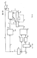
- reference RX denotes a conventional register of the parallel type, synchronous with a clock signal CK (of frequency f cv and period T cv ), able to delay by a time equal to a period T c of sampling frequency f c the binary samples received at the input on connection 1.
- CX operates in the following way: when CX is at logic level "1" register RX stores the sample present at the input on connection 1; when on the contrary CX is at logic level "0" register RX keeps the sample present at the output on connection 2.
- Signals CK and CX examined before correspond respectively to the clock signal and the frame synchronism of PCM and are usually extracted from the flow of the PCM signal within the exchange in which the device object of the invention is inserted.
- Reference S denotes a circuit of known type apt to separate and let through the sign bit with respect to other bits of the samples received at the input, connected to connection 1. It is accepted that the positive or zero value samples correspond to logic value "1" and the negative samples to logic value "0".
- References M1, M2 denotes two circuits of known type apt to separate and let through just the bits coding the modulus of the received samples; the inputs of M 1 and M2 are connected to connections 1 and 2, respectively upstream and downstream RX.
- Reference RI denotes a logic interpolating network able to receive at the input from M 1 and M2 the moduli of two samples subsequent in time, to effect on them suitable arithmetic operations that will be defined hereinafter, and to emit the result at the output on connection 3.
- Reference P denotes a usual EX-OR logic gate.
- Reference GP denotes a circuit able to generate. a pulse, having a duration equal to period T cv of the clock signal, in concomitance with the transitions of the input signal, that GP receives from circuit S, through wire 6.
- Circuits such as GP are well known in the technique.
- Counter C has two outputs: the first, connected to connection 5, supplies a comparator CMP, that will be examined hereinafter, with the contents of the counter itself; the second, connected to wire 8, generates a logic value "1' when the counter reaches the maximum counting value, that in our case is equal to N-1.
- Reference CMP denotes a usual logic comparator able to produce at the output on wire 9 a logic "1" when the binary digits it receives at its two inputs, connected to counter C and to the interpolating network RI, are equal; CMP produces a logic "0" in the opposite case.
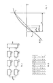
- Reference RS denotes a sequential logic network defined by the table of the transitions and of the outputs represented in Figure 3.
- columns denoted by y and Y represent respectively the present and future states of sequential logic RS ( Figure 2), synchronous with clock signal CK; the columns denoted by 7, 9, 8 represent logic levels present on the input wires of RS, denoted by the same numbers and those denoted by 10, 4 represent the logic levels present on the output wires of RS.
- reference x(t) denotes a sinusoidal signal of analogue type in which some portions of curves have been shown corresponding to the zero-crossing instants and to the sampling instants at which the samples present at the input of circuit SIA or SIB ( Figure 1) are supposed to be extracted; reference T c denotes the period of the sampling frequency; references to, to', to" denote the times elapsing between the sampling instant before a sign change of the sinusoid and the zero-crossing instant.
- function ⁇ 1 (t) represents the trends in time of the sinusoid sign x(t) prior to its sampling
- function ⁇ 2 (t) represents the sign trend of sinusoid x(t) after sampling
- the function ⁇ 3 (t) represents the difference between ⁇ 1 (t), delayed by a sampling period (T c )
- the device object of the present invention overcomes this error, by obtaining an approximate function of ⁇ 1 (t-T c ), hereinafter referred to as ⁇ ' 1 (t-T c ), obtained by the addition of ⁇ 2 (t), that is known, and by an approximate expression ⁇ ' 3 (t) of function ⁇ 3 (1).
- Figure 5 there is represented on an enlarged scale a zero crossing of sinusoid x(t) of Figure 4.
- References x n-1 and x n denote the sample falling respectively before and after the sign change of x(t); to and T c denote the same times as in Figure 4.
- Reference t oa denotes the approximate value of to obtained, as seen in Figure 5, by joining a segment of straight line the points having as ordinates x n-1 and x n .
- Said time t oa can be obtained, by applying the linear- interpolation rules, from the following relationship: where x n and x n-1 denote the absolute values of samples x n and x n-1 .
- the device, object of the present invention generates the waveform ⁇ 3m (t), that is equal to the absolute value of the waveform ⁇ ' 3 (t), and performs the function exclusive-OR between the waveforms ⁇ ' 3m (t) and ⁇ 2 (t) obtaining the wanted waveform ⁇ ' 1 (t-T c ).
- N oa The computation of N oa according to the relationship (3) is performed by logic interpolator network RI of Figure 2.
- Waveform ⁇ ' 3m (t) is originated by circuit RS ( Figure 2) on wire 10 connected to an input of gate P; the waveform ⁇ 2 (t) is originated by circuit S on wire 6, connected to another input of gate P.
- Register RX acts as delay line for a time equal to a sampling interval T e ; in this way on connections 1 and 2 there are always present two subsequent samples of the input signal.
- the values of the moduli of said two samples are present at the outputs of M and M2 while the sign of the present sample is present at the output of S.
- network RI supplies at the output, on connection 3, a number computed on the basis of relation (3).
- Said number has value N oa only in the case when the two examined samples are of the type of x n and x n-1 , that is of opposite sign.
- circuit GP that emits at the output on wire 7 a logic zero whenever at its input, connected to wire 6, a transition occurs from logic value "0" to value "1" " or vice-versa.
- Blocks CMP, C and RS of the diagrams of Figure 2 cooperate to keep, from the instant of the sign change, the output of RS connected to wire 10 at logic level "1" for a time equal to N oa periods of the clock signal CK, that is for a time N oa .T cv , thus producing the waveform ⁇ ' 3m (t) of Figure 4.
Landscapes
- Engineering & Computer Science (AREA)
- Computer Networks & Wireless Communication (AREA)
- Digital Transmission Methods That Use Modulated Carrier Waves (AREA)
- Synchronisation In Digital Transmission Systems (AREA)
Applications Claiming Priority (2)
| Application Number | Priority Date | Filing Date | Title |
|---|---|---|---|
| IT6914979 | 1979-11-05 | ||
| IT69149/79A IT1119943B (it) | 1979-11-05 | 1979-11-05 | Ricevitore di segnali mutlifrequenza di tastiera codificati in pcm |
Publications (2)
| Publication Number | Publication Date |
|---|---|
| EP0028404A1 EP0028404A1 (en) | 1981-05-13 |
| EP0028404B1 true EP0028404B1 (en) | 1983-10-19 |
Family
ID=11311445
Family Applications (1)
| Application Number | Title | Priority Date | Filing Date |
|---|---|---|---|
| EP80106678A Expired EP0028404B1 (en) | 1979-11-05 | 1980-10-31 | Receiver for push-button pcm-encoded multifrequency signals |
Country Status (6)
| Country | Link |
|---|---|
| US (1) | US4379347A (it) |
| EP (1) | EP0028404B1 (it) |
| JP (1) | JPS592234B2 (it) |
| CA (1) | CA1157134A (it) |
| DE (1) | DE3065390D1 (it) |
| IT (1) | IT1119943B (it) |
Families Citing this family (13)
| Publication number | Priority date | Publication date | Assignee | Title |
|---|---|---|---|---|
| JPS6046899B2 (ja) * | 1980-09-26 | 1985-10-18 | 日本電気株式会社 | 反響消去装置 |
| CA1177588A (en) * | 1982-02-12 | 1984-11-06 | Ernst A. Munter | Digital circuit and method for the detection of call progress tones in telephone systems |
| DE3223345A1 (de) * | 1982-06-23 | 1984-01-05 | Philips Patentverwaltung Gmbh, 2000 Hamburg | Verfahren und anordnung zum demodulieren eines frequenzmodulierten eingangssignals |
| US4528664A (en) * | 1982-11-29 | 1985-07-09 | Northern Telecom Limited | Call progress signal monitor and method for telephone systems |
| US4689760A (en) * | 1984-11-09 | 1987-08-25 | Digital Sound Corporation | Digital tone decoder and method of decoding tones using linear prediction coding |
| NL8600889A (nl) * | 1986-04-09 | 1987-11-02 | Philips Nv | Inrichting voor het terugwinnen van kanaalklokinformatie bij synchrone informatietransmissie en een inrichting voor het terugwinnen van de informatie voorzien van een dergelijke inrichting. |
| US5442696A (en) * | 1991-12-31 | 1995-08-15 | At&T Corp. | Method and apparatus for detecting control signals |
| US6429986B1 (en) | 1995-09-07 | 2002-08-06 | International Business Machines Corporation | Data storage to enhance timing recovery in high density magnetic recording |
| KR100276814B1 (ko) * | 1998-12-31 | 2001-01-15 | 윤종용 | 이동통신시스템에서 구성복호기의 상태값 정규화 장치 및방법 |
| KR100326157B1 (ko) | 1998-12-31 | 2002-07-03 | 윤종용 | 통신시스템에서반복디코더에대한양자화방법 |
| US20020049551A1 (en) | 2000-10-20 | 2002-04-25 | Ethicon Endo-Surgery, Inc. | Method for differentiating between burdened and cracked ultrasonically tuned blades |
| TW579498B (en) * | 2001-12-19 | 2004-03-11 | Via Tech Inc | Method for data recovery with lower sampling frequency and related apparatus |
| US6812389B2 (en) | 2003-02-19 | 2004-11-02 | Aaron Rhett Trooien | Locking device for a tremolo |
Family Cites Families (4)
| Publication number | Priority date | Publication date | Assignee | Title |
|---|---|---|---|---|
| NL7511707A (nl) * | 1975-10-06 | 1977-04-12 | Philips Nv | Kruiscorrelatie-inrichting. |
| US4080516A (en) * | 1975-10-06 | 1978-03-21 | Hitachi, Ltd. | Multi-frequency signal receiver |
| US4185172A (en) * | 1976-12-17 | 1980-01-22 | Cselt - Centro Studi E Laboratori Telecomunicazioni S.P.A. | Method of and means for detecting digitized multi frequency-coded signals |
| FR2377729A1 (fr) * | 1977-01-14 | 1978-08-11 | Thomson Csf | Dispositif de decodage de signaux numeriques, et systeme comportant un tel dispositif |
-
1979
- 1979-11-05 IT IT69149/79A patent/IT1119943B/it active
-
1980
- 1980-10-31 DE DE8080106678T patent/DE3065390D1/de not_active Expired
- 1980-10-31 EP EP80106678A patent/EP0028404B1/en not_active Expired
- 1980-11-03 CA CA000363885A patent/CA1157134A/en not_active Expired
- 1980-11-03 US US06/203,459 patent/US4379347A/en not_active Expired - Lifetime
- 1980-11-04 JP JP55153983A patent/JPS592234B2/ja not_active Expired
Also Published As
| Publication number | Publication date |
|---|---|
| DE3065390D1 (en) | 1983-11-24 |
| EP0028404A1 (en) | 1981-05-13 |
| JPS5675793A (en) | 1981-06-23 |
| CA1157134A (en) | 1983-11-15 |
| JPS592234B2 (ja) | 1984-01-17 |
| IT1119943B (it) | 1986-03-19 |
| IT7969149A0 (it) | 1979-11-05 |
| US4379347A (en) | 1983-04-05 |
Similar Documents
| Publication | Publication Date | Title |
|---|---|---|
| EP0028404B1 (en) | Receiver for push-button pcm-encoded multifrequency signals | |
| JP3066213B2 (ja) | 制御信号検出方法 | |
| GB1275446A (en) | Data transmission apparatus | |
| US5333191A (en) | Detection of multifrequency tone signals | |
| US4355405A (en) | Digital signalling system | |
| EP0211865B2 (en) | Supervisory tone detection | |
| US4785255A (en) | Digital FSK signal demodulator | |
| US4395595A (en) | Digital pushbutton signalling receiver | |
| US3404231A (en) | Framing of pulse code transmission systems by use of an added tone signal | |
| US3538256A (en) | Keyboard signalling system | |
| US4293737A (en) | Ringing decoder circuit | |
| US3182127A (en) | Measuring reference distortion of telegraph symbols in start-stop telegraph operation | |
| WO1989012359A1 (fr) | Processeur de signaux | |
| CA1120622A (en) | Single frequency tone receiver | |
| US4009353A (en) | Analog signal detection | |
| US4965811A (en) | Adaptive timing | |
| US3689844A (en) | Digital filter receiver for frequency-shift data signals | |
| US3544723A (en) | Tone detector | |
| JPH0636511B2 (ja) | コード・バイオレーション検出回路 | |
| US5504761A (en) | Apparatus for detecting error in a communications line | |
| EP0124576B1 (en) | Apparatus for receiving high-speed data in packet form | |
| US3622997A (en) | Signal discriminator for time-sharing communication system having periodic line sampling | |
| US3452294A (en) | Digit rate synchronisation of a network of digital stations | |
| SU1496014A1 (ru) | Устройство избирательного вызова | |
| CA1338042C (en) | Adaptive timing |
Legal Events
| Date | Code | Title | Description |
|---|---|---|---|
| PUAI | Public reference made under article 153(3) epc to a published international application that has entered the european phase |
Free format text: ORIGINAL CODE: 0009012 |
|
| AK | Designated contracting states |
Designated state(s): DE FR GB NL SE |
|
| 17P | Request for examination filed |
Effective date: 19810526 |
|
| DET | De: translation of patent claims | ||
| GRAA | (expected) grant |
Free format text: ORIGINAL CODE: 0009210 |
|
| AK | Designated contracting states |
Designated state(s): DE FR GB NL SE |
|
| REF | Corresponds to: |
Ref document number: 3065390 Country of ref document: DE Date of ref document: 19831124 |
|
| ET | Fr: translation filed | ||
| PLBE | No opposition filed within time limit |
Free format text: ORIGINAL CODE: 0009261 |
|
| STAA | Information on the status of an ep patent application or granted ep patent |
Free format text: STATUS: NO OPPOSITION FILED WITHIN TIME LIMIT |
|
| 26N | No opposition filed | ||
| PGFP | Annual fee paid to national office [announced via postgrant information from national office to epo] |
Ref country code: GB Payment date: 19900905 Year of fee payment: 11 |
|
| PGFP | Annual fee paid to national office [announced via postgrant information from national office to epo] |
Ref country code: SE Payment date: 19901016 Year of fee payment: 11 |
|
| PGFP | Annual fee paid to national office [announced via postgrant information from national office to epo] |
Ref country code: NL Payment date: 19901031 Year of fee payment: 11 Ref country code: FR Payment date: 19901031 Year of fee payment: 11 |
|
| PGFP | Annual fee paid to national office [announced via postgrant information from national office to epo] |
Ref country code: DE Payment date: 19901221 Year of fee payment: 11 |
|
| PG25 | Lapsed in a contracting state [announced via postgrant information from national office to epo] |
Ref country code: GB Effective date: 19911031 |
|
| PG25 | Lapsed in a contracting state [announced via postgrant information from national office to epo] |
Ref country code: SE Effective date: 19911101 |
|
| PG25 | Lapsed in a contracting state [announced via postgrant information from national office to epo] |
Ref country code: NL Effective date: 19920501 |
|
| NLV4 | Nl: lapsed or anulled due to non-payment of the annual fee | ||
| PG25 | Lapsed in a contracting state [announced via postgrant information from national office to epo] |
Ref country code: FR Effective date: 19920630 |
|
| GBPC | Gb: european patent ceased through non-payment of renewal fee | ||
| PG25 | Lapsed in a contracting state [announced via postgrant information from national office to epo] |
Ref country code: DE Effective date: 19920701 |
|
| REG | Reference to a national code |
Ref country code: FR Ref legal event code: ST |
|
| EUG | Se: european patent has lapsed |
Ref document number: 80106678.8 Effective date: 19920604 |