EP0025902A2 - Elektrolyt-Kondensator mit niedriger Induktivität - Google Patents
Elektrolyt-Kondensator mit niedriger Induktivität Download PDFInfo
- Publication number
- EP0025902A2 EP0025902A2 EP80105187A EP80105187A EP0025902A2 EP 0025902 A2 EP0025902 A2 EP 0025902A2 EP 80105187 A EP80105187 A EP 80105187A EP 80105187 A EP80105187 A EP 80105187A EP 0025902 A2 EP0025902 A2 EP 0025902A2
- Authority
- EP
- European Patent Office
- Prior art keywords
- terminal
- portions
- capacitor
- case
- header
- Prior art date
- Legal status (The legal status is an assumption and is not a legal conclusion. Google has not performed a legal analysis and makes no representation as to the accuracy of the status listed.)
- Granted
Links
Images

Classifications
-
- H—ELECTRICITY
- H01—ELECTRIC ELEMENTS
- H01G—CAPACITORS; CAPACITORS, RECTIFIERS, DETECTORS, SWITCHING DEVICES, LIGHT-SENSITIVE OR TEMPERATURE-SENSITIVE DEVICES OF THE ELECTROLYTIC TYPE
- H01G9/00—Electrolytic capacitors, rectifiers, detectors, switching devices, light-sensitive or temperature-sensitive devices; Processes of their manufacture
- H01G9/004—Details
- H01G9/04—Electrodes or formation of dielectric layers thereon
- H01G9/06—Mounting in containers
Definitions
- the present invention relates generally to minimizing impedance in capacitors and more particularly to low resistance, low inductance capacitors having low manufacturing casts and high capacitance to volume ratios.
- All capacitors have series equivalent circuits with impedance consisting of capacitance, resistance, and inductance parameters, and conventional electrolytic capacitors have resonant frequencies between 5 and 10 0 kilohertz depending on size, voltage rating, and construction.
- the capacitor impedance is primarily affected by the capacitance and is minimized by maximizing capacitance.
- ESR equivalent series resistance
- the capacitor impedance is primarily affected by the total inductance, or equivalent series inductance (ESL) and is minimized by minimizing the ESL.
- the present invention provides a capacitor and header in which the header carris a pair of spaced apart terminal members which have fully interactive electromagnetic fields when carrying current.
- Each of the terminal members is provided with an input and an output connector lead which are interconnected by parallel and nonparallel terminal portions respectively parallel and nonparallel to corresponding terminal portions on the other terminal portion.
- the present invention further provides that by proximally spacing and juxtapositioning the output connector leads and the parallel terminal portions, and by welding the flat portions of the capacitor element tabs in parallel to the parallel terminal portions, the related electromagnetic fields in this area can be made to neutralize each other resulting in a surprising four fold reduction in ESL at the output connector leads.
- the power from the main power line can now be fed through the capacitor's input connector leads and out the output connector leads to the switching regulated power supply with a minimal ESL while the undesirable ripple and harmonics fed back from the switching regulated power supply are filtered out and prevented from reaching the main power line from the output to the input connector leads because of the higher ESL.
- pulsed power from the switching regulated power supply to the load can be supplied with the minimal ESL and filtered by the higher ESL.
- filter capacitors may be eliminated from the overall power supply, reducing its cost.
- An additional side effect of having four connector leads with two spaced together and two spaced apart is that a generally tripodal configuration is achieved which provides greater mounting stability on printed circuit boards.
- the ends of the tripodal configuration connector leads define three points of a plane which can be matched to the plane of the circuit board.
- An additional side effect inside the capacitor is that the parallel and nonparallel terminal portions effectively extend radially outward from the center of the header so that substantially covering them with the material of the header allows the terminal portions to provide the dual functions of rigidizing the header while providing interiorly extending ribs which engage the capacitor element to prevent radial movement thereof when subject to vibration.
- the terminal members may be made of copper, or aluminium with a suitable plating.
- FIG. 1 therein is shown an electrolytic capacitor 10 having a capacitor case 12 which contains a capacitor element 14.
- the capacitor element 14 is made up of a first , spacer film 16 abutting and encircling a first electrode film 18 which in turn encircles and abuts a second spacer film 20.
- the second spacer film 20 further encircles and abuts a second electrode film 22.
- the first and second spacer films 16 and 20 are saturated in a conventional manner with a conventional capacitor electrolyte.
- the first electrode film 18, the cathode has a first tab 24 electrically and conductively abutting it and extending from it towards the open end of the capacitor case 12.
- the second electrode film 22, the anode has a second tab 26 electrically conductively and abutting it and extending therefrom.
- the first and second tabs 24 and 26 are flat, rectangular shaped pieces of a conductive material, such as aluminum, which are deformable as well as weldable.
- The.capacitor case 12 is sealed by a header 28 (shown removed) which is made of a nonconductive moldable material in the preferred embodiment.
- the header can be made of a conductive material such as aluminum if proper insulation for the anode parts is provided.
- the header 28 is held in place, to seal off the open end of the capacitor case 12, by being inserted in the capacitor cas 12 and then having the case's edge rolled over a rim on the header 28 to prevent outward movement thereof.
- Fig. 1 Also shown in Fig. 1 are a pair of parallel output connector leads 32 and 34 which are proximally spaced and a pair of parallel input connector leads 36 and 38 which are distally spaced. These leads will be described in greater detail later.
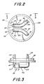
- Fig. 2 therein is shown the header 28 as seen from inside of the capacitor case 12.
- the first and second tabs 24 and 26 are shown respectively welded by welds 30 and 31 to respective first and second terminal members 40 and 42.
- the first and second terminal members have respective parallel terminal portions 44 and 46 which are spaced apart and parallel, and nonparallel terminal portions 48 and 50 which are spaced apart and nonparallel.
- the nonparallel terminal portions 48 and 50 diverge toward their respective connections to the input connector leads 36 and 38.
- header ribs 52 and 54 which are extensions of the header material around the portion of the first and second terminal members 40 and 42 which are inside of the capacitor case 12. It will be noted . that the header ribs 52 and 54 do not extend completely over the parallel terminal portions 44 and 46 respectively so that the first and second tabs 24 and 26 may be respectively welded in parallel directly to the case proximal sides of the terminal members.
- Fig. 3 therein may be seen the second terminal member 42 with the second tab 26 affixed by weld 31 on to the case-proximate-surface of the parallel terminal portion 46. Also therein may be seen the integral output and input connctor leads 34 and 38 which are portions of the second terminal member 42. Similarly, the output and input connector leads 32 and 36 are integral portions of the first terminal member 40.
- the terminal members are made of aluminum while the connector leads may be solid copper but are preferably splash-coated with copper.
- the reason for copper is tht while aluminum is inexpensive compared to copper, it can only be welded and cannot be soldered as required in most electrical applications.
- the required connection of the tabs can be done in the factory during manufacture and the aluminum allows low cost terminals while the copper allows the capacitor 10 to be soldered on to electrical circuit boards in a customer's factory.
- the elctrolytic capacitor 10 is mounted on circuit boards of a switching regulated power supply system (not shown).
- a switching regulated power supply system (not shown).
- such a system consists of a full wave rectifier connected in parallel with a first filter capacitor, to a transistor switching circuit.
- the transistor switch circuit is connected through a series inductance with a second filter capacitor to a direct current load.
- the output of the full wave rectifier is filtered by the first filter capacitor and is chopped by the transistor switching circuit into a pulse train.
- the series inductance and the parallel second filter capacitor integrates the pulse train to provide the D.C. output.
- the frequency or duty cycle of the switching regulated power supply is varied to maintain the output at the desired level.
- the electrolytic capacitor 10 as the second filter capacitor between the series inductance and the load acts as a filter capacitor. It is connected with the input connector leads 38 and 36 respectively connected to the inductance and the transistor switching circuit.
- the output connector leads 32 and 34 are connected to the load.
- the low inductance output out of the output connector leads 32 and 34 provides a substantially constant, low voltage D. C. output while the higher inductance on the input adds to the series inductance to help filter out the undesirable harmonic andripple components of the output.
- the electrolytic capacitor 10 as the first capacitor between the full wave rectifier and the transistor switch circuit is connected with the output connector leads 36 and 38 connected to the rectifier and the input connector leads 32 and 34 connected to the transistor switch circuit.
- the capacitor is used to convert the full wave rectified output to a high voltage D. C. output while the higher inductance filters out the high frequency harmonics and ripple from the transistor switch circuit from feeding back into the main power supply which is generally a 60 cycle A. C. source.
- the parallel terminal portions 4 4 and 46 of the terminal members 40 and 42 as well as the output connector leads 32 and 34 were placed in parallel to neutralize the interaction of electromagnetic fields therebetween and minimize the capacitor output inductance. Basically, this works because the electromagnetic field of any given conductor may be neutralized by passing an equal current in the opposite direction through a second conductor parallel and close to the given conductor.
- the above further affords a means for controlling the inductance to a slightly higher level by causing the wires to be nonparallel and diverge by a controlled amount as desired by a particular application.
- the terminal members 40 and 42 are respectively provided with the nonparallel terminal portions 48 and 50.
- the welds 30 and 31 are made from the sides of the capacitor element 14 to the case-proximate portions of the parallel terminal portions 44 and 46. This allows the first and second tabs 24 and 26 to be of a minimumlength because the header 28 does not have to be pivoted up for welding.
- ESR equivalent series resistance
- An additional advantage of the above arrangement is the possibility of reducing the overall size of the capacitor to increase capacitance to volume ratio by providing the largest capacitance in the smallest volume. Less volume is required for the tabs and the inward extension of the terminal members can be minimized.
- ESL equivalent series inductance
- the header ribs 52 and 54 are formed of header material covering over the case-interior portions of the first and second terminal members 40 and 42.
- the header ribts 52 and 54 will indent the capacitor element 14 as it is compressed against the closed end of the capacitor case 12. This indentation of the capacitor element 14 will prevent relative radial as well as axial movement between the capacitor element 14 and the header 28 so as to prevent flexure and subsequent breakage of the first and second tabs 24 and 26.
Landscapes
- Engineering & Computer Science (AREA)
- Power Engineering (AREA)
- Microelectronics & Electronic Packaging (AREA)
- Fixed Capacitors And Capacitor Manufacturing Machines (AREA)
Applications Claiming Priority (2)
| Application Number | Priority Date | Filing Date | Title |
|---|---|---|---|
| US06/074,175 US4314313A (en) | 1979-09-10 | 1979-09-10 | Single and dual low inductance capacitor and header therefor |
| US74175 | 1979-09-10 |
Publications (3)
| Publication Number | Publication Date |
|---|---|
| EP0025902A2 true EP0025902A2 (de) | 1981-04-01 |
| EP0025902A3 EP0025902A3 (en) | 1982-05-12 |
| EP0025902B1 EP0025902B1 (de) | 1985-12-11 |
Family
ID=22118135
Family Applications (1)
| Application Number | Title | Priority Date | Filing Date |
|---|---|---|---|
| EP80105187A Expired EP0025902B1 (de) | 1979-09-10 | 1980-09-01 | Elektrolyt-Kondensator mit niedriger Induktivität |
Country Status (5)
| Country | Link |
|---|---|
| US (1) | US4314313A (de) |
| EP (1) | EP0025902B1 (de) |
| JP (1) | JPS5698812A (de) |
| CA (1) | CA1152170A (de) |
| DE (1) | DE3071287D1 (de) |
Cited By (1)
| Publication number | Priority date | Publication date | Assignee | Title |
|---|---|---|---|---|
| DE102012208474A1 (de) * | 2012-05-21 | 2013-11-21 | Robert Bosch Gmbh | Axialer Kondensator |
Families Citing this family (3)
| Publication number | Priority date | Publication date | Assignee | Title |
|---|---|---|---|---|
| TW502859U (en) * | 2001-08-03 | 2002-09-11 | Chieh-Fu Lin | Chip-type capacitor structure |
| US6529365B1 (en) | 2001-09-28 | 2003-03-04 | Intel Corporation | Multiple terminal SMT BGA-style wound capacitor |
| JP4161589B2 (ja) * | 2002-02-20 | 2008-10-08 | 株式会社日立製作所 | 低電圧用コンデンサ |
Family Cites Families (11)
| Publication number | Priority date | Publication date | Assignee | Title |
|---|---|---|---|---|
| US3654524A (en) * | 1970-03-13 | 1972-04-04 | Sprague Electric Co | Electrolytic book capacitor |
| JPS5230946B2 (de) * | 1972-07-05 | 1977-08-11 | ||
| US3806770A (en) * | 1973-02-21 | 1974-04-23 | Mallory & Co Inc P R | Electrical capacitor with non-inductive leads |
| US3822397A (en) * | 1973-05-07 | 1974-07-02 | Sprague Electric Co | A capacitor package with a split metal-plate terminal cover |
| FR2232825B1 (de) * | 1973-06-07 | 1978-06-30 | Sic Safco Condensateurs | |
| DE2406141B2 (de) * | 1974-02-08 | 1976-10-21 | Siemens AG, 1000 Berlin und 8000 München | Elektrolytkondensator und seine verwendung |
| US3971970A (en) * | 1974-11-27 | 1976-07-27 | P. R. Mallory & Co., Inc. | Electrical component with low impedance at high frequency |
| US4001656A (en) * | 1974-12-27 | 1977-01-04 | P. R. Mallory & Co., Inc. | Capacitor having a plurality of anode risers for low impedance at high frequency |
| JPS5537852B2 (de) * | 1975-02-14 | 1980-09-30 | ||
| US4097916A (en) * | 1976-06-28 | 1978-06-27 | Union Carbide Corporation | Electrolytic capacitor lead terminal configuration |
| DE3032819A1 (de) * | 1979-09-04 | 1981-03-19 | North American Philips Corp., New York, N.Y. | Kondensator mit bandleitungsanschluessen |
-
1979
- 1979-09-10 US US06/074,175 patent/US4314313A/en not_active Expired - Lifetime
-
1980
- 1980-09-01 DE DE8080105187T patent/DE3071287D1/de not_active Expired
- 1980-09-01 EP EP80105187A patent/EP0025902B1/de not_active Expired
- 1980-09-09 CA CA000359930A patent/CA1152170A/en not_active Expired
- 1980-09-09 JP JP12520680A patent/JPS5698812A/ja active Pending
Cited By (1)
| Publication number | Priority date | Publication date | Assignee | Title |
|---|---|---|---|---|
| DE102012208474A1 (de) * | 2012-05-21 | 2013-11-21 | Robert Bosch Gmbh | Axialer Kondensator |
Also Published As
| Publication number | Publication date |
|---|---|
| CA1152170A (en) | 1983-08-16 |
| EP0025902B1 (de) | 1985-12-11 |
| US4314313A (en) | 1982-02-02 |
| JPS5698812A (en) | 1981-08-08 |
| DE3071287D1 (en) | 1986-01-23 |
| EP0025902A3 (en) | 1982-05-12 |
Similar Documents
| Publication | Publication Date | Title |
|---|---|---|
| US4298906A (en) | Capacitor and element therefor | |
| US4314313A (en) | Single and dual low inductance capacitor and header therefor | |
| US20240097301A1 (en) | Integrated Choke Assembly | |
| JP3587333B2 (ja) | コンデンサ素子の端子構造 | |
| JP3805507B2 (ja) | コンデンサ | |
| US4141070A (en) | Electrolytic capacitors | |
| US6563692B2 (en) | Capacitor | |
| JP6961111B2 (ja) | 電力供給装置およびコンデンサ | |
| CA1165413A (en) | Low inductance electrolytic capacitor | |
| JPS5932123Y2 (ja) | 貫通電極シ−ルド型電解コンデンサ | |
| JPS5919433Y2 (ja) | 4端子形電解コンデンサ | |
| JP4245360B2 (ja) | L−c型のフィルタモジュール、および少なくとも2個のこのようなモジュールからなるヘリコイダルフィルタ | |
| JPS584186Y2 (ja) | デンカイコンデンサ | |
| JPS6015331Y2 (ja) | 電解コンデンサ | |
| JPS6038282Y2 (ja) | 電解コンデンサ | |
| JPS6035234Y2 (ja) | 4端子型電解コンデンサ | |
| US4814939A (en) | Capacitor with integral tab arbor | |
| JPH0536266Y2 (de) | ||
| JPS5918670Y2 (ja) | 電解コンデンサ | |
| JP2867554B2 (ja) | 偏平形アルミ電解コンデンサ | |
| JPS6127174Y2 (de) | ||
| JPS593565Y2 (ja) | デンカイコンデンサ | |
| JPS647486B2 (de) | ||
| JPS5833701Y2 (ja) | 低インピ−ダンス電解コンデンサ | |
| JPH03277170A (ja) | オーディオ用電源平滑装置 |
Legal Events
| Date | Code | Title | Description |
|---|---|---|---|
| PUAI | Public reference made under article 153(3) epc to a published international application that has entered the european phase |
Free format text: ORIGINAL CODE: 0009012 |
|
| AK | Designated contracting states |
Designated state(s): DE FR GB NL SE |
|
| PUAL | Search report despatched |
Free format text: ORIGINAL CODE: 0009013 |
|
| AK | Designated contracting states |
Designated state(s): DE FR GB NL SE |
|
| 17P | Request for examination filed |
Effective date: 19821029 |
|
| GRAA | (expected) grant |
Free format text: ORIGINAL CODE: 0009210 |
|
| AK | Designated contracting states |
Designated state(s): DE FR GB NL SE |
|
| REF | Corresponds to: |
Ref document number: 3071287 Country of ref document: DE Date of ref document: 19860123 |
|
| ET | Fr: translation filed | ||
| PGFP | Annual fee paid to national office [announced via postgrant information from national office to epo] |
Ref country code: NL Payment date: 19860930 Year of fee payment: 7 |
|
| PLBE | No opposition filed within time limit |
Free format text: ORIGINAL CODE: 0009261 |
|
| STAA | Information on the status of an ep patent application or granted ep patent |
Free format text: STATUS: NO OPPOSITION FILED WITHIN TIME LIMIT |
|
| 26N | No opposition filed | ||
| PG25 | Lapsed in a contracting state [announced via postgrant information from national office to epo] |
Ref country code: SE Effective date: 19870902 |
|
| PG25 | Lapsed in a contracting state [announced via postgrant information from national office to epo] |
Ref country code: NL Effective date: 19880401 |
|
| GBPC | Gb: european patent ceased through non-payment of renewal fee | ||
| NLV4 | Nl: lapsed or anulled due to non-payment of the annual fee | ||
| PG25 | Lapsed in a contracting state [announced via postgrant information from national office to epo] |
Ref country code: FR Free format text: LAPSE BECAUSE OF NON-PAYMENT OF DUE FEES Effective date: 19880531 |
|
| PG25 | Lapsed in a contracting state [announced via postgrant information from national office to epo] |
Ref country code: DE Effective date: 19880601 |
|
| REG | Reference to a national code |
Ref country code: FR Ref legal event code: ST |
|
| PG25 | Lapsed in a contracting state [announced via postgrant information from national office to epo] |
Ref country code: GB Free format text: LAPSE BECAUSE OF NON-PAYMENT OF DUE FEES Effective date: 19881118 |
|
| EUG | Se: european patent has lapsed |
Ref document number: 80105187.1 Effective date: 19880906 |