EP0025324B1 - Semiconductor light-emitting device - Google Patents
Semiconductor light-emitting device Download PDFInfo
- Publication number
- EP0025324B1 EP0025324B1 EP80303019A EP80303019A EP0025324B1 EP 0025324 B1 EP0025324 B1 EP 0025324B1 EP 80303019 A EP80303019 A EP 80303019A EP 80303019 A EP80303019 A EP 80303019A EP 0025324 B1 EP0025324 B1 EP 0025324B1
- Authority
- EP
- European Patent Office
- Prior art keywords
- light
- crystal layer
- emitting device
- groove
- launching
- Prior art date
- Legal status (The legal status is an assumption and is not a legal conclusion. Google has not performed a legal analysis and makes no representation as to the accuracy of the status listed.)
- Expired
Links
Images


Classifications
-
- H—ELECTRICITY
- H10—SEMICONDUCTOR DEVICES; ELECTRIC SOLID-STATE DEVICES NOT OTHERWISE PROVIDED FOR
- H10H—INORGANIC LIGHT-EMITTING SEMICONDUCTOR DEVICES HAVING POTENTIAL BARRIERS
- H10H20/00—Individual inorganic light-emitting semiconductor devices having potential barriers, e.g. light-emitting diodes [LED]
- H10H20/80—Constructional details
- H10H20/81—Bodies
- H10H20/819—Bodies characterised by their shape, e.g. curved or truncated substrates
- H10H20/821—Bodies characterised by their shape, e.g. curved or truncated substrates of the light-emitting regions, e.g. non-planar junctions
-
- G—PHYSICS
- G02—OPTICS
- G02B—OPTICAL ELEMENTS, SYSTEMS OR APPARATUS
- G02B6/00—Light guides; Structural details of arrangements comprising light guides and other optical elements, e.g. couplings
- G02B6/24—Coupling light guides
- G02B6/42—Coupling light guides with opto-electronic elements
- G02B6/4201—Packages, e.g. shape, construction, internal or external details
- G02B6/4202—Packages, e.g. shape, construction, internal or external details for coupling an active element with fibres without intermediate optical elements, e.g. fibres with plane ends, fibres with shaped ends, bundles
- G02B6/4203—Optical features
-
- G—PHYSICS
- G02—OPTICS
- G02B—OPTICAL ELEMENTS, SYSTEMS OR APPARATUS
- G02B6/00—Light guides; Structural details of arrangements comprising light guides and other optical elements, e.g. couplings
- G02B6/24—Coupling light guides
- G02B6/42—Coupling light guides with opto-electronic elements
- G02B6/4201—Packages, e.g. shape, construction, internal or external details
- G02B6/4204—Packages, e.g. shape, construction, internal or external details the coupling comprising intermediate optical elements, e.g. lenses, holograms
- G02B6/4206—Optical features
-
- H—ELECTRICITY
- H10—SEMICONDUCTOR DEVICES; ELECTRIC SOLID-STATE DEVICES NOT OTHERWISE PROVIDED FOR
- H10H—INORGANIC LIGHT-EMITTING SEMICONDUCTOR DEVICES HAVING POTENTIAL BARRIERS
- H10H20/00—Individual inorganic light-emitting semiconductor devices having potential barriers, e.g. light-emitting diodes [LED]
- H10H20/80—Constructional details
- H10H20/85—Packages
- H10H20/855—Optical field-shaping means, e.g. lenses
Definitions
- This invention relates to a semiconductor light-emitting device, and more particularly to a light-emitting diode (LED) preferably used for optical communication in which a launching efficiency, that is, the ratio of the quantity of radiation transferred through an optical fiber to the total quantity of radiation emitted from the light-emitting portion of the LED, is increased.
- a launching efficiency that is, the ratio of the quantity of radiation transferred through an optical fiber to the total quantity of radiation emitted from the light-emitting portion of the LED, is increased.
- the critical angle at a plane surface of the crystal that is, the minimum angle for total reflection
- the critical angle is about 16°, and thus, only 1.4% of the light emitted from the LED is obtained outside the crystal.
- an optical fiber for transferring the light emitted from the LED is of a plane-ended type, only incident rays within an acceptance angle on the plane-ended surface can be incident to the fiber. Therefore, only about 2 percent of the divergent rays emitted from the plane surface of the crystal is incident to the fiber.
- a so-called spherical-ended fiber In order to increase the quantity of rays injected into an optical fiber, a so-called spherical-ended fiber, the end of which is manufactured as a sphere, is used.
- a so-called spherical-ended fiber is expensive.
- it is very difficult to do so especially when LEDs are arranged in an array.
- the term "launching efficiency" used hereinafter is defined as the ratio of the incident optical power into a fibre to the generated optical power in an LED.
- An object of the present invention is to provide an LED in which the launching efficiency is improved, especially into a plane-ended optical fibre.
- a semiconductor light-emitting device comprising a semi-conductor substrate, and a semiconductor crystal layer formed by epitaxial growth on the surface of the substrate, characterized in that successively grown regions of the layer have increasing refractive indices, and further comprising a light-emitting portion formed in a region of relatively high refractive index in the crystal layer, wherein light emitted from the said portion is continuously refracted in the crystal layer and emerges from the device through a light-launching surface as a beam with a resulting increased maximum radiation angle.
- the x value may be gradually decreased during the epitaxial growth to increase the refractive index.
- the semi-conductor substrate has a groove in its surface and the crystal layer fills the groove so that the shape of the groove determines the contours of regions having the same x-value in the crystal layer formed on the said surface.
- this groove is of semi-circular cross-section.
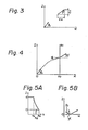
- Fig. 1A is a general side view of an LED for explaining the principle of the present invention.
- an LED 11 is comprised of a substrate 1 of GaAs and a crystal layer of Ga 1 - x Al x As having a thickness of about 30 through 60 pm.
- the crystal layer is manufacturd by liquid-phase epitaxial growth.
- the x values in the crystal layer 2 are different dependent on the positions in the crystal layer 2.
- the dotted lines in Fig. 1A represent equi-index lines of refraction.
- the distribution of the x values with respect to the depth of the crystal layer 2 is illustrated in Fig. 1B by a solid curve.
- the x value is increased in accordance with the increase of the depth.
- the refractive indices vary with respect to the depth of the crystal layer 2.
- the refractive index is decreased along with the increase of the depth.
- the launching efficiency which is the ratio of the quantity of light launched from a light-emitting device to the total quantity of light generated in the light-emitting device, can be improved.
- Fig. 2 illustrates a trace of a light ray launched from an LED and incident upon an optical fiber, for explaining the launching efficiency when the refractive index in the LED is constant.
- an optical fiber 12 of a step-index type faces the LED 11.
- the optical fiber 12 is comprised of a core 12A and a cladding 12B.
- the refractive index of the LED 11 in Fig. 2 is constant and represented as no.
- the refractive indices of the core 12A and the cladding 12B are n 1 and n 2 , respectively.
- the refractive index of the medium between the LED 11 and the fiber 12 is n . .
- the incident angle at the side surface 2b is 0o.
- the angle of refraction at the light-launching surface 2b which is equal to the angle of incidence at the incident surface 12b of the fiber 12, is ⁇ c .
- the angle of refraction at the incident surface 12b of the core 12A of the fiber 12 is ⁇ 1 .
- the angle of incidence at the boundary surface between the core 12A and the cladding 12B is, therefore, 90°- ⁇ 1 .
- the angle of refraction at the boundary surface is 90°- ⁇ 2 . According to the Snell's law, the following expressions (1) and (2) are obtained. In order to transfer a light ray through the core 12A of the fiber 12, the light ray must be reflected at the boundary surface.
- the critical angle ⁇ c max of the angle ⁇ c is obtained by substituting ⁇ 1 max for the angle ⁇ 1 in the expression (2) and can be expressed as:
- NA represents the numerical aperture and is expressed as:
- An incident-light ray from the medium into the core 12A of the fiber 12 can be transferred through the core 12A if the incident angle is smaller than the critical angle ⁇ c max.
- the critical angle ⁇ 0 max of the angle of incidence at the light-launching surface 2b can be expressed as:
- the critical angle ⁇ 0 max does not depend on the refractive index n c of the medium.
- the launching efficiency ⁇ which is the ratio of the quantity of radiation transferred through the core 12A of the fiber 12 to the total quantity of radiation emitted from the light-emitting portion of the LED, can be defined as the ratio of the solid angle of the critical angle ⁇ 0 max, which is equal to 2n(1-cos ⁇ o max), to the total solid angle 4n. Therefore, the launching efficiency n can be expressed as:
- the critical angle ⁇ 0 max is equal to 2.58° and the launching efficiency is equal to 0.000507.
- the launching efficiency ⁇ is increased to a value of 0.001016, which is only the double of the above mentioned value of 0.000507. Accordingly, 99.9% of the quantity of light emitted from the light-emitting portion of the LED cannot be incident into the optical fiber.
- the refractive index n in the crystal layer of an LED and, accordingly, the x value of the crystal layer are dependent only on the positions along the thickness of the crystal layer.
- the abscissa indicates the x value and the ordinate indicates the position Z along the thickness of the crystal layer.
- the angle of incidence ⁇ r and the angle of refraction ⁇ r ' at the boundary surface can be expressed as: and n no -gx r
- the light rays which fulfil the expression can reach the boundary surface between the side surfaces of the crystal layer 2 and the core 12A before the light rays collide against the surface of the light-adsorbing medium.
- the discriminant of the quadratic equation: must be negative. Therefore, the relation: can be obtained.
- the angle ⁇ 0 is positive, the expression: is obtained.
- ⁇ 0 max can be determined as: Also, by substituting the value ⁇ 0 in the expression (19) for the above practical value of 10.62°, and by assuming that NA in the expression (19) is equal to 0.16, the maximum length of the crystal layer 2 in the transverse direction is: If the length of the crystal layer is larger than the maximum length X,max, the radiation angle ⁇ o must be larger than the maximum radiation angle ⁇ 0 max in order for the emitted light ray to reach the light-launching surface 2b before the light ray collides against the light-adsorbing surface.
- Fig. 6 is a graph illustrating the relation between the maximum radiation angle ⁇ 0 max and the maximum length X r max, under the conditions that the numerical aperture NA is equal to 0.16 and the refractive index no is equal to 3.55.
- the refractive index n d is 3.3
- the maximum radiation angle 4)0 max is 10.62°
- the maximum length X is 100.71 micrometers, as illustrated by a dotted line.
- the corresponding values of n d , ⁇ 0 max and X r max can be determined in a similar way by using Fig. 6.
- the maximum radiation angle ⁇ 0 max of 10.62° in the condition of the expression (14) is about four times larger than the maximum radiation angle ⁇ 0 max of 2.58° in the condition that the refraction index no is constant in the crystal layer.
- the refractive index n o ' In order to totally reflect the light rays emitted with a radiation angle - ⁇ larger than the angle - ⁇ 0 max at the boundary surface, the refractive index n o ' must fulfil the condition: When the above-mentioned practical values are applied to the expression (23), the refractive index n o ' is smaller than the value 3.489.
- the light-emitting surface may be made of metal evaporation surface.
- Fig. 7 illustrates the light-launching surface 2b of the LED 11 of Fig. 1A.
- dotted lines parallel to the surface of the substrate 1 represent equi-index lines of refraction. Referring to Figs. 1A and 7, the surfaces of equi-index of refraction are parallel to the surface of the substrate.
- the light-launching surface 2b Because of this fact, among the light rays emitted from the light emitting portion 2a toward the substrate 1, only a small quantity of light can reach the light-launching surface 2b.
- the light rays which can reach the side surface 2b are those emitted at an angle within a critical angle a o between the vertical line VI-VI and a side 4 of a triangle forming the slashed area.
- the other light rays emitted at an angle larger than the critical angle a o can not reach the light-launching surface 2b. Therefore, by the structure of the LED illustrated in Fig. 7, the launching efficiency is limited.
- An ideal structure for obtaining large launching efficiency is illustrated in Fig. 8. As illustrated in Fig. 8 by dotted lines, the equi-index lines of refraction should be concentric in the ideal structure. However, it is difficult to manufacture the crystal layer 2 so as to have such concentric equi-index lines of refraction.
- a groove is formed on the surface of the substrate so that the equi-index surfaces of refraction become simiar to concentric surfaces.
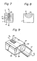
- Fig. 9 illustrates a perspective view of an LED according to the first embodiment of the present invention.
- the LED of this first embodiment comprises an n-type GaAs substrate 21 and an n-type Ga 1-x Al x As crystal layer 22 formed on the substrate 21.
- a groove 28 having a cross section of a half circle is formed on the surface of the substrate 21.
- the groove 28 extends from the rear surface to the light-launching surface.
- the crystal layer 22 is formed by epitaxial growth on the groove 28, so that the x values are gradually decreased in accordance with the increase of the thickness of the crystal layer 22.
- An insulating film 24, such as silicon dioxide, is formed on the crystal layer 22.
- a positive electrode 25 is formed through a contact window formed in the insulating film 24.
- a negative electrode 26 is formed under the GaAs substrate 21.
- An optical fiber 27 is faced to a light launching surface of the LED.
- Fig. 10 is a cross-sectional view taken along the line X-X of Fig. 9.
- a p-type impurity diffusion region 23 is formed by diffusing zinc in a part of the upper portion of the crystal layer 22.
- a light-emitting portion 23A is provided in the region 23.
- the light rays emitted from the light-emitting portion 23A toward the substrate 21 are bent due to the distribution of refractive indices, and a part of the light rays are incident through the light-launching surface into the optical fiber 27.
- the light rays emitted from the light-emitting portion 23A toward the insulating film 24 are reflected by the electrode 25 (see light paths II).
- the insulating film 24 is made of transparent material, total reflection mainly occurs at the surface of the electrode 25.
- Fig. 11 illustrates a partial cross-sectional view taken along the line XI-XI of Fig. 10.
- the groove 28 at the top surface of the substrate 21 has a cross section of a half circle.
- the dotted lines represent equi-index lines of refraction. Due to the structure of the groove 28, the equi-index lines of refraction are similar to concentric circles. Therefore, the light rays which can reach the launching surface 29 are those emitted at an angle within a critical angle ⁇ as illustrated in Fig. 11.
- the angle ⁇ is much larger than the angle a o in Fig. 7. Therefore, according to this first embodiment, the launching efficiency is greatly increased in comparison with the example of Fig. 7.
- the launching efficiency ⁇ I ⁇ obtained by this first embodiment is 0.00428, which is 4.2 times as large as the conventional launching efficiency of 0.001016.
- Fig. 12 is a graph illustrating the relation between the refractive index and the x value for a light ray with a wave length of 0.812 micrometer, in the Ga 1 - x Al x As crystal layer 22 used in this first embodiment.
- the minimum x value is nearly equal to 0.05.
- the minimum x value nearly corresponds to the energy gap for transferring the light ray. Therefore, a region having an x value lower than 0.05 is not transparent for light rays.
- refractive indices decrease according to the increase of x values.
- Fig. 13 is a graph illustrating the best mode of the distribution of x values with respect to the depth of the crystal layer 22.
- the Ga 1-x Al x As crystal layer 22 is formed on the GaAs substrate 21 by liquid-phase epitaxial growth under the condition that the speed of decreasing the temperature of the crystal is 0.3°C per minute, the starting temperature for the epitaxial growth is 900°C, and the time duration for the epitaxial growth is 3.5 hours.
- the crystal layer 22 is grown to have a thickness of about 50 micrometers.
- the distance between the light-emitting portion 23A and the launching surface 29 (Fig. 10) is preferably about 100 micrometers.
- the segregation factor of AlAs is larger than that of GaAs, the quantity of aluminium in the Gallium solution, and therefore, the x value, is decreased in accordance with the development of the epitaxial growth.
- the decrease in the x value is smaller in a shallow area of the crystal layer 22 than in a deep area. Therefore, the distribution curve of the x value with respect to the depth of the crystal layer 22 is similar to a parabolic curve.
- the distribution curve of the refractive indexes is also similar to a parabolic curve. The distribution curve similar to the parabolic curve corresponds to the parabolic trace of the light path illustrated in Fig. 4.
- the added layer can be used as a reflection layer.
- the added layer is also used as a layer for trapping injected carriers in the layer itsets during the operation of the LED.
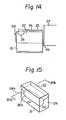
- Fig. 14 is a general side view of an LED according to the second embodiment of the present invention.
- the structure of this LED is quite similar to that of the LED of the first embodiment.
- the only difference between Fig. 10 and Fig. 14 is that, in Fig. 14, a reflecting film 28 is provided on the basic surface opposite to the light-launching surface 29 of the crystal layer 22, so that the launching efficiency is increased to two times that of the first embodiment.
- the launching efficiency r l2 obtained by the LED of this second embodiment is 0.00856, which is 8.4 times are larger as the conventional launching efficiency of 0.001016.
- Fig. 15 is a partial perspective view of an LED according to the third embodiment of the invention.
- the structure of this LED is almost the same as that of the LED of Fig. 10.
- the only difference between Fig. 10 and Fig. 15 is that, in Fig. 15, a groove 28a terminates with a curved surface 28b, before the groove 28a reaches the back side surface opposite the light launching surface 29.
- the equi-index surfaces of refraction of the Ga 1 - x Al x As crystal layer 12 formed on the groove 28a are similar to the curved surfaces 28b.
- Fig. 16 is a schematic diagram illustrating equi-index lines of refraction, when seen from the cross section (a) of Fig. 15.
- the equi-index lines are curved along the curved surface 28b of the groove 28a, Therefore, a light path B in the area where the equi-index lines are curved is bent more than a light path A in the area where the equi-index lines are parallel to each other.
- the light-emitting portion 23A is preferably formed at the top surface of the crystal layer 22 and at the portion near the curved surface 28b of the end of the groove 28a, as illustrated in Fig. 16.
- the maximum radiation angle, when the light-emitting portion 23A is formed at the above mentioned position, is represented by ⁇ ' 0 max, which is larger than the maximum radiation angle ⁇ o max when the light emitting portion 23A is formed at a portion where the equi-index lines are parallel.
- Fig. 17 is a schematic diagram illustrating equi-index lines of refraction when seen from the cross section taken along the line XVII-XVII of Fig. 16.
- a light ray C emitted downward from the light-emitting portion 23A is bent toward the light-launching surface 29 (Fig. 15). If a cross section is taken along the line XVII'-XVII' the density of the equi-index lines becomes higher than the density as illustrated in Fig. 7. Therefore, a light ray D emitted to a direction having a transverse component is bent so that the transverse component is decreased.
- the groove 28a extends throughout the surface of the substrate 21, such as in the aforementioned first and second embodiments, the light rays are bent so as to be parallel to the equi-index surfaces of refraction, as illustrated in Fig. 17 by a dotted line D'. Therefore, according to this third embodiment, light rays are bent more sharply than in the first and second embodiments, in which the groove has no end, resulting in an improved launching efficiency.
- the groove has a cross section of a half circle in the foregoing preferred embodiments, alternatively, the cross section may have any shape, such as a shape of a half ellipse, V-shape, a trapezoid, etc.
- a heterojunction such as a diffused-type single heterostructure or a grown junction type single heterostructure
- a heterojunction such as a diffused-type single heterostructure or a grown junction type single heterostructure
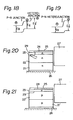
- Fig. 18 is a schematic diagram illustrating an energy level of the diffused-type single heterostructure. As will be seen from Fig. 18, electrons injected from a p-n junction in a p-type region are prevented from diffusing by a heterojunction. The quantity of holes injected into the n-type region is increased by decreasing the distance between the p-n junction and the heterojunction.
- Fig. 19 is a schematic diagram illustrating an energy level of the grown-junction type single heterostructure. As will be seen from Fig. 19, only electrons are injected from the n-type trapping region.
- the energy gap in the heterojunction must be more than 3KT (where, K is the Bolzman constant and T is an absolute temperature).
- K is the Bolzman constant and T is an absolute temperature.
- the x value at the light-emitting portion is 0.05
- the x value of the trapping layer must be more than 0.15.
- the x value of 0.15 is sufficient for the total reflection layer.
- Fig. 20 is a cross sectional view of an LED when its light-emitting portion utilizes the diffused-type single heterostructure.
- the numeral 29 represents an n-type Ga 1 - x Al x As crystal layer formed after growing the crystal layer 22.
- the crystal layer 29 is used as an electron-trapping layer, as well as a reflecting layer as previously mentioned in conjunction with .
- Fig. 21 is a cross sectional view of an LED when its light-emitting portion utilizes the grown-junction type single heterostructure. Referring to Fig. 21, a p-type Ga 1 - x Al x As crystal layer 22' is formed on a p-type GaAs substrate.
- the conduction type may be changed from n to p and from p to n.
- an array of several LED's may be placed against a plane-ended optical fibre.
- the light-launching efficiency is improved and a large quantity of light can be incident in an optical fibre without using a spherical-ended fibre.
Landscapes
- Physics & Mathematics (AREA)
- General Physics & Mathematics (AREA)
- Optics & Photonics (AREA)
- Led Devices (AREA)
- Liquid Deposition Of Substances Of Which Semiconductor Devices Are Composed (AREA)
- Semiconductor Lasers (AREA)
Applications Claiming Priority (2)
| Application Number | Priority Date | Filing Date | Title |
|---|---|---|---|
| JP11115979A JPS5642388A (en) | 1979-08-31 | 1979-08-31 | Semiconductor light emitting device |
| JP111159/79 | 1979-08-31 |
Publications (3)
| Publication Number | Publication Date |
|---|---|
| EP0025324A2 EP0025324A2 (en) | 1981-03-18 |
| EP0025324A3 EP0025324A3 (en) | 1983-02-02 |
| EP0025324B1 true EP0025324B1 (en) | 1985-12-27 |
Family
ID=14553967
Family Applications (1)
| Application Number | Title | Priority Date | Filing Date |
|---|---|---|---|
| EP80303019A Expired EP0025324B1 (en) | 1979-08-31 | 1980-08-29 | Semiconductor light-emitting device |
Country Status (4)
| Country | Link |
|---|---|
| US (1) | US4354199A (enExample) |
| EP (1) | EP0025324B1 (enExample) |
| JP (1) | JPS5642388A (enExample) |
| DE (1) | DE3071309D1 (enExample) |
Families Citing this family (5)
| Publication number | Priority date | Publication date | Assignee | Title |
|---|---|---|---|---|
| JP2579326B2 (ja) * | 1987-11-13 | 1997-02-05 | 三菱化学株式会社 | エピタキシャル・ウエハ及び発光ダイオード |
| US4861976A (en) * | 1988-06-06 | 1989-08-29 | American Telephone And Telegraph Company, At&T Bell Laboratories | Optical or opto-electronic device having a trapping layer in contact with a semiconductive layer |
| JPH0327577A (ja) * | 1989-06-23 | 1991-02-05 | イーストマン・コダックジャパン株式会社 | 発光ダイオ―ドアレイ |
| JP2003168822A (ja) * | 2001-11-30 | 2003-06-13 | Shin Etsu Handotai Co Ltd | 発光素子及びその製造方法 |
| JP4293178B2 (ja) * | 2005-11-09 | 2009-07-08 | パナソニック電工株式会社 | 立体回路基板の製造方法 |
Family Cites Families (5)
| Publication number | Priority date | Publication date | Assignee | Title |
|---|---|---|---|---|
| US3790853A (en) * | 1973-01-19 | 1974-02-05 | Rca Corp | Semiconductor light ray deflector |
| US4025157A (en) * | 1975-06-26 | 1977-05-24 | The United States Of America As Represented By The Secretary Of The Navy | Gradient index miniature coupling lens |
| US4117504A (en) * | 1976-08-06 | 1978-09-26 | Vadim Nikolaevich Maslov | Heterogeneous semiconductor structure with composition gradient and method for producing same |
| FR2404307A1 (fr) * | 1977-09-27 | 1979-04-20 | Centre Nat Etd Spatiales | Cellules solaires a double heterojonction et dispositif de montage |
| US4294510A (en) * | 1979-12-10 | 1981-10-13 | International Business Machines Corporation | Semiconductor fiber optical detection |
-
1979
- 1979-08-31 JP JP11115979A patent/JPS5642388A/ja active Granted
-
1980
- 1980-08-29 DE DE8080303019T patent/DE3071309D1/de not_active Expired
- 1980-08-29 EP EP80303019A patent/EP0025324B1/en not_active Expired
- 1980-08-29 US US06/182,587 patent/US4354199A/en not_active Expired - Lifetime
Non-Patent Citations (1)
| Title |
|---|
| IBM TECHNICAL DISCLOSURE BULLETIN, vol. 21, no. 3, August 1978, page 1260, New York (USA); D. BOTEX et al.: "Channel waveguide A1GaAs edge emitting led" * |
Also Published As
| Publication number | Publication date |
|---|---|
| EP0025324A2 (en) | 1981-03-18 |
| US4354199A (en) | 1982-10-12 |
| DE3071309D1 (en) | 1986-02-06 |
| JPS5642388A (en) | 1981-04-20 |
| EP0025324A3 (en) | 1983-02-02 |
| JPS6138873B2 (enExample) | 1986-09-01 |
Similar Documents
| Publication | Publication Date | Title |
|---|---|---|
| US5705834A (en) | Increased efficiency LED | |
| US5162878A (en) | Light-emitting diode array with projections | |
| US12278313B2 (en) | Light-emitting device with internal non-specular light redirection and anti-reflective exit surface | |
| US4279690A (en) | High-radiance emitters with integral microlens | |
| EP0174344B1 (en) | Edge-emitting light emitting diode | |
| US6995030B2 (en) | Semiconductor chip for optoelectronics | |
| US8183587B2 (en) | LED with upstanding nanowire structure and method of producing such | |
| CA1147050A (en) | Light emitting diode and method of making the same | |
| CA1298645C (en) | Super-luminescent diode | |
| US4958355A (en) | High performance angled stripe superluminescent diode | |
| KR20070042938A (ko) | 발광 다이오드 구조체 및 그의 형성 방법 | |
| JP2003017740A (ja) | 光取出率を改善するための発光デバイスにおける光学エレメントの形成 | |
| KR100532281B1 (ko) | 면굴절 입사형 수광소자 및 그 제조방법 | |
| WO2019021362A1 (ja) | 端面入射型受光素子 | |
| EP0025324B1 (en) | Semiconductor light-emitting device | |
| JP2806423B2 (ja) | 面発光型半導体素子 | |
| JPH1012929A (ja) | 発光ダイオードの実装構造 | |
| KR100464333B1 (ko) | 수광소자 및 그 제조방법 | |
| JPS59205774A (ja) | 半導体発光素子 | |
| RU2055420C1 (ru) | Светоизлучающий диод | |
| CN114927602B (zh) | 微型发光二极管芯片及其制备方法 | |
| EP0772248A2 (en) | Microactivity LED with photon recycling | |
| JPS6120156B2 (enExample) | ||
| US11268676B2 (en) | Light-emitting device assembly with light redirection or incidence-angle-dependent transmission through an escape surface | |
| US6392283B1 (en) | Photodetecting device and method of manufacturing the same |
Legal Events
| Date | Code | Title | Description |
|---|---|---|---|
| PUAI | Public reference made under article 153(3) epc to a published international application that has entered the european phase |
Free format text: ORIGINAL CODE: 0009012 |
|
| 17P | Request for examination filed |
Effective date: 19800905 |
|
| AK | Designated contracting states |
Designated state(s): DE FR GB NL |
|
| PUAL | Search report despatched |
Free format text: ORIGINAL CODE: 0009013 |
|
| AK | Designated contracting states |
Designated state(s): DE FR GB NL |
|
| GRAA | (expected) grant |
Free format text: ORIGINAL CODE: 0009210 |
|
| AK | Designated contracting states |
Designated state(s): DE FR GB NL |
|
| ET | Fr: translation filed | ||
| REF | Corresponds to: |
Ref document number: 3071309 Country of ref document: DE Date of ref document: 19860206 |
|
| PLBE | No opposition filed within time limit |
Free format text: ORIGINAL CODE: 0009261 |
|
| STAA | Information on the status of an ep patent application or granted ep patent |
Free format text: STATUS: NO OPPOSITION FILED WITHIN TIME LIMIT |
|
| 26N | No opposition filed | ||
| PGFP | Annual fee paid to national office [announced via postgrant information from national office to epo] |
Ref country code: GB Payment date: 19890831 Year of fee payment: 10 |
|
| PG25 | Lapsed in a contracting state [announced via postgrant information from national office to epo] |
Ref country code: GB Effective date: 19900829 |
|
| PGFP | Annual fee paid to national office [announced via postgrant information from national office to epo] |
Ref country code: FR Payment date: 19900830 Year of fee payment: 11 |
|
| PGFP | Annual fee paid to national office [announced via postgrant information from national office to epo] |
Ref country code: NL Payment date: 19900831 Year of fee payment: 11 |
|
| PGFP | Annual fee paid to national office [announced via postgrant information from national office to epo] |
Ref country code: DE Payment date: 19901024 Year of fee payment: 11 |
|
| GBPC | Gb: european patent ceased through non-payment of renewal fee | ||
| PG25 | Lapsed in a contracting state [announced via postgrant information from national office to epo] |
Ref country code: NL Effective date: 19920301 |
|
| NLV4 | Nl: lapsed or anulled due to non-payment of the annual fee | ||
| PG25 | Lapsed in a contracting state [announced via postgrant information from national office to epo] |
Ref country code: FR Effective date: 19920430 |
|
| PG25 | Lapsed in a contracting state [announced via postgrant information from national office to epo] |
Ref country code: DE Effective date: 19920501 |
|
| REG | Reference to a national code |
Ref country code: FR Ref legal event code: ST |