EP0772248A2 - Microactivity LED with photon recycling - Google Patents
Microactivity LED with photon recycling Download PDFInfo
- Publication number
- EP0772248A2 EP0772248A2 EP96116891A EP96116891A EP0772248A2 EP 0772248 A2 EP0772248 A2 EP 0772248A2 EP 96116891 A EP96116891 A EP 96116891A EP 96116891 A EP96116891 A EP 96116891A EP 0772248 A2 EP0772248 A2 EP 0772248A2
- Authority
- EP
- European Patent Office
- Prior art keywords
- led
- mesa
- layer
- layers
- photon recycling
- Prior art date
- Legal status (The legal status is an assumption and is not a legal conclusion. Google has not performed a legal analysis and makes no representation as to the accuracy of the status listed.)
- Granted
Links
Images
Classifications
-
- H—ELECTRICITY
- H01—ELECTRIC ELEMENTS
- H01S—DEVICES USING THE PROCESS OF LIGHT AMPLIFICATION BY STIMULATED EMISSION OF RADIATION [LASER] TO AMPLIFY OR GENERATE LIGHT; DEVICES USING STIMULATED EMISSION OF ELECTROMAGNETIC RADIATION IN WAVE RANGES OTHER THAN OPTICAL
- H01S5/00—Semiconductor lasers
- H01S5/02—Structural details or components not essential to laser action
- H01S5/024—Arrangements for thermal management
-
- H—ELECTRICITY
- H01—ELECTRIC ELEMENTS
- H01L—SEMICONDUCTOR DEVICES NOT COVERED BY CLASS H10
- H01L33/00—Semiconductor devices with at least one potential-jump barrier or surface barrier specially adapted for light emission; Processes or apparatus specially adapted for the manufacture or treatment thereof or of parts thereof; Details thereof
- H01L33/02—Semiconductor devices with at least one potential-jump barrier or surface barrier specially adapted for light emission; Processes or apparatus specially adapted for the manufacture or treatment thereof or of parts thereof; Details thereof characterised by the semiconductor bodies
- H01L33/10—Semiconductor devices with at least one potential-jump barrier or surface barrier specially adapted for light emission; Processes or apparatus specially adapted for the manufacture or treatment thereof or of parts thereof; Details thereof characterised by the semiconductor bodies with a light reflecting structure, e.g. semiconductor Bragg reflector
- H01L33/105—Semiconductor devices with at least one potential-jump barrier or surface barrier specially adapted for light emission; Processes or apparatus specially adapted for the manufacture or treatment thereof or of parts thereof; Details thereof characterised by the semiconductor bodies with a light reflecting structure, e.g. semiconductor Bragg reflector with a resonant cavity structure
-
- H—ELECTRICITY
- H01—ELECTRIC ELEMENTS
- H01L—SEMICONDUCTOR DEVICES NOT COVERED BY CLASS H10
- H01L33/00—Semiconductor devices with at least one potential-jump barrier or surface barrier specially adapted for light emission; Processes or apparatus specially adapted for the manufacture or treatment thereof or of parts thereof; Details thereof
- H01L33/36—Semiconductor devices with at least one potential-jump barrier or surface barrier specially adapted for light emission; Processes or apparatus specially adapted for the manufacture or treatment thereof or of parts thereof; Details thereof characterised by the electrodes
- H01L33/40—Materials therefor
- H01L33/405—Reflective materials
-
- H—ELECTRICITY
- H01—ELECTRIC ELEMENTS
- H01L—SEMICONDUCTOR DEVICES NOT COVERED BY CLASS H10
- H01L33/00—Semiconductor devices with at least one potential-jump barrier or surface barrier specially adapted for light emission; Processes or apparatus specially adapted for the manufacture or treatment thereof or of parts thereof; Details thereof
- H01L33/44—Semiconductor devices with at least one potential-jump barrier or surface barrier specially adapted for light emission; Processes or apparatus specially adapted for the manufacture or treatment thereof or of parts thereof; Details thereof characterised by the coatings, e.g. passivation layer or anti-reflective coating
- H01L33/46—Reflective coating, e.g. dielectric Bragg reflector
- H01L33/465—Reflective coating, e.g. dielectric Bragg reflector with a resonant cavity structure
Definitions
- This invention relates to light emitting diodes (LED) and more specifically to a LED with improved light emission and efficiency.
- the efficiency of a LED is limited by the total internal reflection because the index of refraction of the semiconductor material making up the LED (typically 3 - 3.5) is much higher than the index of refraction of the air (1) into which the light is emitted.
- Light distribution external to a LED is generally referred to as a Lambertian distribution, and corresponds to an omnidirectional distribution internal to the device. Because of this large spatial distribution of the generated light, only small amounts of the light can be effectively utilized, especially if the light is going to be coupled to a light conduction medium such as an optical fiber.
- a Lambertian source such as a LED
- Increased efficiency implies less current and, therefore, less power to couple the same amount of light to a system.
- a more efficient LED provides higher optical coupling and less stringent specifications on the coupling designs and procedures, which results in less expensive and more manufacturable systems. These reasons imply that if the efficiency of a LED can be increased then the device will become more useful in applied technology.
- One method to improve the external efficiency of an LED is to utilize reflectors on all sides of the LED except the light emitting side as disclosed in U.S. patent No. 5,358,880, entitled Method of Manufacturing Closed Cavity LED, issued 25 October, 1994 and assigned to the same assignee. In this manner, generated photons are directed in a single general direction. While increasing the efficiency of an LED, photons propagated in or near the plane of the device will be emitted at an oblique angle. The emission angle of these photons prevents their acceptance by a coupling to an optical system.
- LEDs require large drive currents to generate enough light so that a reasonable amount of light couples to an optical fiber. With improved efficiencies, less current is required and, therefore, less heat is generated. Thus, a LED with improved efficiency results in greater applicability of the LED for commercial use.
- Another object of the invention is to provide an LED with improved light emitting characteristics and improved efficiency.
- Another object of the invention is to provide a LED with reduced output angle of photons for improved optical coupling.
- a microcavity LED with photon recycling including a substrate having at least one layer of semiconductor material positioned thereon, a first cladding layer of a first conductivity type positioned on the layer of material, an active region positioned on the first cladding region, a second cladding layer of a second conductivity type positioned on the active region, the first cladding layer, the active region and the second cladding layer forming a mesa on the layer of material, the mesa having generally vertical sides and an upper surface, and an electrically conductive and light reflective system positioned on a layer of dielectric material and partially covering the upper surface to form a first electrical contact for the LED, the electrically conductive and light reflective system defining a centrally located light emitting opening on the surface of the mesa, the mesa having a diametric dimension on the surface in the range of 2 to 10 times larger than a diametric dimension of the opening.
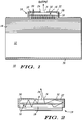
- Fig. 1 illustrates a LED generally designated 10.
- the device of the present invention consists of at least one layer, in this embodiment a plurality of layers, formed on a substrate 12 of a suitable material.
- the various layers are formed by epitaxial deposition accomplished by well known techniques in the art such as MBE, MOCVD, CBE, or the like. These techniques enable epitaxial depositions of relatively thin and thick layers of materials such as gallium arsenide, aluminum gallium arsenide, aluminum arsenide, silicon, indium gallium arsenide, etc.
- substrate 12 is gallium arsenide (GaAs) or the like which, as will be understood presently, is compatible with layers subsequently grown thereon.
- GaAs gallium arsenide
- Mirror stack 14 is generally formed, for example, by epitaxially growing a plurality of pairs of layers of semiconductor material with alternating indexes of refraction on substrate 12.
- Each pair of alternating layers are grown to a predetermined thickness (approximately one half wavelength at the operating frequency) and the number of pairs is chosen to provide as much reflectivity of light as possible while limiting the stack to a practical number. In the preferred embodiment, approximately 30 pairs of layers are used for purposes described subsequently in the specification.
- An active region 16 generally including one or more quantum wells separated by barrier layers is grown on mirror stack 14 with a spacer or cladding layer on either side thereof.
- the quantum wells, barrier layers and cladding layers are grown epitaxially.
- the quantum wells produce photons (light) in accordance with a well known phenomenon when properly energized by electrical current applied thereacross. In general, the greater the current applied to active region 16 the greater the number of photons generated.
- a layer is deposited over mirror stack 14 and forms a cladding layer 18 of the first conductivity type in LED 10.
- Cladding layer 18 is lightly doped with an impurity to produce the first conductivity type.
- Three layers 20 of undoped material cooperate to provide active region 16 of LED 10. It should be understood that additional layers may be added to provide additional quantum wells as desired.
- a second cladding layer 22 is deposited on the upper surface of active region 16 and is lightly doped with an impurity to produce a second conductivity type.
- Layers 20 forming active region 16 and cladding layers 18 and 22 on either side thereof form the light generating portion of LED 10.
- Layers 18, 20 and 22 form what is commonly referred to as the cavity of the LED and is the light generating portion of LED 10.
- the cavity is made very short, employing thin, lightly doped cladding layers, so that the internal free carrier loss is small, thereby increasing the efficiency.
- the formation of mirror stack 14 and active region 16 is well known in the art and will not be elaborated upon further in this disclosure.
- Cladding layers 18 and 22 and active region 16 are formed into a mesa 24 on mirror stack 14 by conventional etching techniques.
- Mesa 24 has an upper surface 26 and substantially vertical sides 28.
- a dielectric layer 30 is deposited on the top surface of mirror stack 14 and vertical sides 28 of mesa 24.
- Dielectric layer 30 may be substantially any of the well known materials such as silicon nitride (SiN x ), and prevents electrical current from entering LED 10 from anywhere except the upper surface of mesa and causing a short in the LED.
- a first metal contact layer 32 is deposited on the upper surface of cladding layer 22 and on dielectric layer 30 over vertical sides 28 and mirror stack 14.
- First metal contact layer 32 forms an ohmic contact with cladding layer 22.
- first metal contact layer 32 is formed of titanium tungsten (TiW) because it is convenient to deposit and is a p-type contact metal compatible with cladding layer 22.
- dielectric layer 30 and first metal contact layer 32 form an electrically conductive and light reflective system.
- the electrically conductive and light reflective system may include reflective material on the sides of the mesa and an electrically conductive and reflective material on the upper surface, or some other variations thereof.
- First metal contact layer 32 is deposited over the entire upper surface and sides of LED 10 (on the outside of dielectric layer 30) except for a light emitting opening 34 centrally located on upper surface 26.
- First metal contact layer 32 and mirror stack 14 form a reflective cavity to reflect light (photons) in all directions until they exit through light emitting opening 34.
- Light emitting opening 34 restricts the photon emission angle resulting in the emission of photons which increases the coupling efficiency of the LED.
- Light emitting opening 34 is significantly smaller than the upper surface of mesa 24, with upper surface of mesa 24 having a diametric dimension 2-10 times larger than the diametric dimension of light emitting opening 34.
- Adjusting the relative sizes of light emitting opening 34 and size of mesa 24 allows adjustment of the average number of recycling events and hence the photon lifetime of the device. Also, because a greater area of the upper mesa surface is contacted by first metal contact layer 32, better electrical contact is provided and better current distribution in the LED is realized.
- a Second contact layer 36 is deposited on the lower surface of substrate 12.
- Second contact layer 36 is shown as a n-type metal, and is the opposing contact to First metal contact layer 32.
- Current passed between first metal contact layer 32 and second contact layer 36 generates photons within active region 16 as described previously.
- second contact layer 36 may be positioned in different locations as desired, such as between substrate 12 and mirror stack 14. Since second contact layer 36 need not have light reflective characteristics, it may be a highly doped semiconductor material instead of metal.
- photons are generated by recombination of carriers injected into active region 16. Many of the photons traveling perpendicular to the surface of substrate 12 can couple efficiently into the optical mode defined by mirror stack 14 and first metal contact layer 32. In other words, photons which are generally perpendicular to substrate 12 and which are centrally generated, will be emitted through light emitting opening 34. Photons which are generated at an angle or which are not generated centrally will be reflected back into active region 16 as shown in FIG. 2. The reflected photons are then absorbed into active region 16 and re-emitted in a different direction in what is well known as the photon recycling process. This process continues until the photon is emitted through light emitting opening 34.
Abstract
Description
- This invention relates to light emitting diodes (LED) and more specifically to a LED with improved light emission and efficiency.
- The efficiency of a LED is limited by the total internal reflection because the index of refraction of the semiconductor material making up the LED (typically 3 - 3.5) is much higher than the index of refraction of the air (1) into which the light is emitted. Light distribution external to a LED is generally referred to as a Lambertian distribution, and corresponds to an omnidirectional distribution internal to the device. Because of this large spatial distribution of the generated light, only small amounts of the light can be effectively utilized, especially if the light is going to be coupled to a light conduction medium such as an optical fiber. In dealing with a Lambertian source, such as a LED, there are many ways available today to provide a method to increase the light coupling from the LED to the fiber core. For example, spherical lenses, microlenses, gradient index lenses (GRIN), diffraction gratings all are utilized successfully. Unfortunately, none of these techniques actually increases the amount of light generated for the same input current.
- Increased efficiency implies less current and, therefore, less power to couple the same amount of light to a system. A more efficient LED provides higher optical coupling and less stringent specifications on the coupling designs and procedures, which results in less expensive and more manufacturable systems. These reasons imply that if the efficiency of a LED can be increased then the device will become more useful in applied technology.
- One method to improve the external efficiency of an LED is to utilize reflectors on all sides of the LED except the light emitting side as disclosed in U.S. patent No. 5,358,880, entitled Method of Manufacturing Closed Cavity LED, issued 25 October, 1994 and assigned to the same assignee. In this manner, generated photons are directed in a single general direction. While increasing the efficiency of an LED, photons propagated in or near the plane of the device will be emitted at an oblique angle. The emission angle of these photons prevents their acceptance by a coupling to an optical system.
- Currently, LEDs require large drive currents to generate enough light so that a reasonable amount of light couples to an optical fiber. With improved efficiencies, less current is required and, therefore, less heat is generated. Thus, a LED with improved efficiency results in greater applicability of the LED for commercial use.
- It would be highly advantageous, therefore, to remedy the foregoing and other deficiencies inherent in the prior art.
- Accordingly, it is an object of the present invention to provide improvements in LEDs.
- Another object of the invention is to provide an LED with improved light emitting characteristics and improved efficiency.
- And another object of the invention is to provide a LED with reduced output angle of photons for improved optical coupling.
- Briefly, to achieve the desired objects of the instant invention in accordance with a preferred embodiment thereof, provided is a microcavity LED with photon recycling including a substrate having at least one layer of semiconductor material positioned thereon, a first cladding layer of a first conductivity type positioned on the layer of material, an active region positioned on the first cladding region, a second cladding layer of a second conductivity type positioned on the active region, the first cladding layer, the active region and the second cladding layer forming a mesa on the layer of material, the mesa having generally vertical sides and an upper surface, and an electrically conductive and light reflective system positioned on a layer of dielectric material and partially covering the upper surface to form a first electrical contact for the LED, the electrically conductive and light reflective system defining a centrally located light emitting opening on the surface of the mesa, the mesa having a diametric dimension on the surface in the range of 2 to 10 times larger than a diametric dimension of the opening.
- The foregoing and further and more specific objects and advantages of the instant invention will become readily apparent to those skilled in the art from the following detailed description of a preferred embodiment thereof taken in conjunction with the drawings, in which:
- FIG. 1 is a sectional side view of an LED constructed in accordance with the teachings of the present invention; and
- FIG. 2 is an enlarged sectional view of a portion of the LED illustrated in FIG. 1, illustrating photon recycling.
- Turning now to the drawings in which like reference characters indicate corresponding elements throughout the several views, attention is first directed to Fig. 1, which illustrates a LED generally designated 10. The device of the present invention consists of at least one layer, in this embodiment a plurality of layers, formed on a
substrate 12 of a suitable material. Generally, the various layers are formed by epitaxial deposition accomplished by well known techniques in the art such as MBE, MOCVD, CBE, or the like. These techniques enable epitaxial depositions of relatively thin and thick layers of materials such as gallium arsenide, aluminum gallium arsenide, aluminum arsenide, silicon, indium gallium arsenide, etc. - Generally,
substrate 12 is gallium arsenide (GaAs) or the like which, as will be understood presently, is compatible with layers subsequently grown thereon. Amirror stack 14 of Bragg mirrors having a first conductivity type, which in this specific embodiment is n-type conductivity, is grown on an upper surface ofsubstrate 12. It should be understood that an intermediate layer or layers, such as a buffer layer, could be included as a portion ofsubstrate 12.Mirror stack 14 is generally formed, for example, by epitaxially growing a plurality of pairs of layers of semiconductor material with alternating indexes of refraction onsubstrate 12. Each pair of alternating layers are grown to a predetermined thickness (approximately one half wavelength at the operating frequency) and the number of pairs is chosen to provide as much reflectivity of light as possible while limiting the stack to a practical number. In the preferred embodiment, approximately 30 pairs of layers are used for purposes described subsequently in the specification. - An
active region 16 generally including one or more quantum wells separated by barrier layers is grown onmirror stack 14 with a spacer or cladding layer on either side thereof. The quantum wells, barrier layers and cladding layers are grown epitaxially. The quantum wells produce photons (light) in accordance with a well known phenomenon when properly energized by electrical current applied thereacross. In general, the greater the current applied toactive region 16 the greater the number of photons generated. - In the preferred embodiment, a layer is deposited over
mirror stack 14 and forms acladding layer 18 of the first conductivity type inLED 10. Claddinglayer 18 is lightly doped with an impurity to produce the first conductivity type. Threelayers 20 of undoped material cooperate to provideactive region 16 ofLED 10. It should be understood that additional layers may be added to provide additional quantum wells as desired. Asecond cladding layer 22 is deposited on the upper surface ofactive region 16 and is lightly doped with an impurity to produce a second conductivity type.Layers 20 formingactive region 16 and claddinglayers LED 10.Layers LED 10. In the present embodiment ofLED 10 the cavity is made very short, employing thin, lightly doped cladding layers, so that the internal free carrier loss is small, thereby increasing the efficiency. The formation ofmirror stack 14 andactive region 16 is well known in the art and will not be elaborated upon further in this disclosure. - Cladding
layers active region 16 are formed into amesa 24 onmirror stack 14 by conventional etching techniques. Mesa 24 has anupper surface 26 and substantiallyvertical sides 28. Adielectric layer 30 is deposited on the top surface ofmirror stack 14 andvertical sides 28 ofmesa 24.Dielectric layer 30 may be substantially any of the well known materials such as silicon nitride (SiNx), and prevents electrical current from enteringLED 10 from anywhere except the upper surface of mesa and causing a short in the LED. - A first
metal contact layer 32 is deposited on the upper surface ofcladding layer 22 and ondielectric layer 30 oververtical sides 28 andmirror stack 14. Firstmetal contact layer 32 forms an ohmic contact withcladding layer 22. In this specific embodiment firstmetal contact layer 32 is formed of titanium tungsten (TiW) because it is convenient to deposit and is a p-type contact metal compatible withcladding layer 22. In this embodimentdielectric layer 30 and firstmetal contact layer 32 form an electrically conductive and light reflective system. However, in other applications the electrically conductive and light reflective system may include reflective material on the sides of the mesa and an electrically conductive and reflective material on the upper surface, or some other variations thereof. - First
metal contact layer 32 is deposited over the entire upper surface and sides of LED 10 (on the outside of dielectric layer 30) except for a light emitting opening 34 centrally located onupper surface 26. Firstmetal contact layer 32 andmirror stack 14 form a reflective cavity to reflect light (photons) in all directions until they exit through light emitting opening 34. Light emitting opening 34 restricts the photon emission angle resulting in the emission of photons which increases the coupling efficiency of the LED.Light emitting opening 34 is significantly smaller than the upper surface ofmesa 24, with upper surface ofmesa 24 having a diametric dimension 2-10 times larger than the diametric dimension oflight emitting opening 34. Adjusting the relative sizes oflight emitting opening 34 and size of mesa 24 (upper surface and depth) allows adjustment of the average number of recycling events and hence the photon lifetime of the device. Also, because a greater area of the upper mesa surface is contacted by firstmetal contact layer 32, better electrical contact is provided and better current distribution in the LED is realized. - A
Second contact layer 36 is deposited on the lower surface ofsubstrate 12.Second contact layer 36 is shown as a n-type metal, and is the opposing contact to Firstmetal contact layer 32. Current passed between firstmetal contact layer 32 andsecond contact layer 36 generates photons withinactive region 16 as described previously. It will be understood thatsecond contact layer 36 may be positioned in different locations as desired, such as betweensubstrate 12 andmirror stack 14. Sincesecond contact layer 36 need not have light reflective characteristics, it may be a highly doped semiconductor material instead of metal. - In operation, photons are generated by recombination of carriers injected into
active region 16. Many of the photons traveling perpendicular to the surface ofsubstrate 12 can couple efficiently into the optical mode defined bymirror stack 14 and firstmetal contact layer 32. In other words, photons which are generally perpendicular tosubstrate 12 and which are centrally generated, will be emitted throughlight emitting opening 34. Photons which are generated at an angle or which are not generated centrally will be reflected back intoactive region 16 as shown in FIG. 2. The reflected photons are then absorbed intoactive region 16 and re-emitted in a different direction in what is well known as the photon recycling process. This process continues until the photon is emitted throughlight emitting opening 34. - In order for the photon recycling process to work efficiently, free carrier absorption and scattering losses need to be minimized. This is achieved by making
cladding layers mirror stack 14 so that the acceptance angle for high reflectivity is large. In the preferred embodiment, approximately 30 mirror pairs are employed, providing reflectivity of >>99% for all incident angles <16 degrees. Thus provided is an LED with high efficiency and with a photon output angle which increases coupling to optical systems, further increases the apparent efficiency. - Various changes and modifications to the embodiments herein chosen for purposes of illustration will readily occur to those skilled in the art. To the extent that such modifications and variations do not depart from the spirit of the invention, they are intended to be included within the scope thereof which is assessed only by a fair interpretation of the following claims.
- Having fully described the invention in such clear and concise terms as to enable those skilled in the art to understand and practice the same, the invention claimed is:
Claims (9)
- A microcavity LED with photon recycling characterized by:a substrate (12) having at least one layer (14) of material positioned thereon;a first cladding layer (18) of a first conductivity type positioned on the layer (14) of material;an active region (16) positioned on the first cladding layer (18);a second cladding layer (22) of a second conductivity type positioned on the active region (16);the first cladding layer (18), the active region (16) and the second cladding layer (22) forming a mesa (24) on the layer (14) of material, the mesa (24) having generally vertical sides (28) and an upper surface (26); andan electrically conductive and light reflective system (32) positioned on the vertical sides (28) of the mesa (24) and partially covering the upper surface (26) to form a first electrical contact for the LED (10), the electrically conductive and light reflective system (32) defining a centrally located light emitting opening (34) on the surface (26) of the mesa (24), the mesa (24) having a diametric dimension of the surface (26) greater than one time larger than a diametric dimension of the opening (34).
- A microcavity LED with photon recycling as claimed in claim 1 further characterized in that the at least one layer (14) of material includes a mirror stack (14).
- A microcavity LED with photon recycling as claimed in claim 2 further characterized in that the mirror stack (14) includes approximately thirty pairs of layers.
- A microcavity LED with photon recycling as claimed in claim 3 further characterized in that the thirty pairs of layers each include layers of AlGaAs.
- A microcavity LED with photon recycling as claimed in claim 4 further characterized in that the thirty pairs of layers each include layers of different amounts of aluminum to provide different indexes of refraction.
- A microcavity LED with photon recycling as claimed in claim 1 further characterized in that the electrically conductive and light reflective system (32) includes a dielectric layer (30) deposited on the vertical sidewalls (28) of the mesa (24), and a first metal contact layer (32) deposited on the dielectric layer (30) and on the upper surface (26).
- A microcavity LED with photon recycling as claimed in claim 6 further characterized in that the cladding layers (18, 22) are thin and lightly doped to reduce internal free carrier loss.
- A microcavity LED with photon recycling as claimed in claim 7 further characterized in that the active region (18) includes a plurality of quantum well layers (20) separated by barrier layers.
- A microcavity LED with photon recycling as claimed in claim 1 further characterized in that the diametric diameter of the surface of the mesa (24) is in the range of 2 to 10 times larger than the diametric dimension of the light emitting opening (34).
Applications Claiming Priority (2)
| Application Number | Priority Date | Filing Date | Title |
|---|---|---|---|
| US08/550,147 US5710441A (en) | 1995-10-30 | 1995-10-30 | Microcavity LED with photon recycling |
| US550147 | 1995-10-30 |
Publications (3)
| Publication Number | Publication Date |
|---|---|
| EP0772248A2 true EP0772248A2 (en) | 1997-05-07 |
| EP0772248A3 EP0772248A3 (en) | 1997-07-02 |
| EP0772248B1 EP0772248B1 (en) | 2002-05-02 |
Family
ID=24195938
Family Applications (1)
| Application Number | Title | Priority Date | Filing Date |
|---|---|---|---|
| EP96116891A Expired - Lifetime EP0772248B1 (en) | 1995-10-30 | 1996-10-21 | Microactivity LED with photon recycling |
Country Status (5)
| Country | Link |
|---|---|
| US (1) | US5710441A (en) |
| EP (1) | EP0772248B1 (en) |
| KR (1) | KR100413708B1 (en) |
| DE (1) | DE69620975T2 (en) |
| TW (1) | TW320783B (en) |
Cited By (6)
| Publication number | Priority date | Publication date | Assignee | Title |
|---|---|---|---|---|
| WO2000045443A1 (en) * | 1999-01-28 | 2000-08-03 | Nova Crystals, Inc. | High performance light emitting diodes |
| US6576933B2 (en) * | 2000-03-10 | 2003-06-10 | Kabushiki Kaisha Toshiba | Semiconductor light emitting device and method for manufacturing same |
| DE102006041460A1 (en) * | 2006-09-04 | 2008-03-13 | Osram Opto Semiconductors Gmbh | Radiation emitting semiconductor chip, has semiconductor layer sequence with active area for producing electromagnetic radiation, which is arranged between base and side surfaces, and reflecting layer is applied on base and side surfaces |
| DE102007046519A1 (en) * | 2007-09-28 | 2009-04-02 | Osram Opto Semiconductors Gmbh | Thin-film LED with a mirror layer and method for its production |
| US8120049B2 (en) * | 2007-06-22 | 2012-02-21 | Sanken Electric Co., Ltd. | Light-emitting semiconductor device |
| EP1416545B1 (en) * | 2002-10-29 | 2015-04-29 | Philips Lumileds Lighting Company LLC | Enhanced brightness light emitting device spot emitter |
Families Citing this family (6)
| Publication number | Priority date | Publication date | Assignee | Title |
|---|---|---|---|---|
| US5892786A (en) * | 1997-03-26 | 1999-04-06 | The United States Of America As Represented By The Secretary Of The Air Force | Output control of vertical microcavity light emitting device |
| US6630689B2 (en) * | 2001-05-09 | 2003-10-07 | Lumileds Lighting, U.S. Llc | Semiconductor LED flip-chip with high reflectivity dielectric coating on the mesa |
| WO2005071452A1 (en) * | 2004-01-23 | 2005-08-04 | Koninklijke Philips Electronics, N.V. | Seamlessly integrated optical wave guide for light generated by a semiconductor light source |
| TW200537143A (en) * | 2004-02-11 | 2005-11-16 | Koninkl Philips Electronics Nv | Integrated optical wave guide for light generated by a bipolar transistor |
| TW200602585A (en) * | 2004-03-16 | 2006-01-16 | Koninkl Philips Electronics Nv | High brightness illumination device with incoherent solid state light source |
| JP5038147B2 (en) * | 2004-11-18 | 2012-10-03 | コーニンクレッカ フィリップス エレクトロニクス エヌ ヴィ | Luminescent body and method for producing the luminous body |
Citations (3)
| Publication number | Priority date | Publication date | Assignee | Title |
|---|---|---|---|---|
| JPS60253286A (en) * | 1984-05-29 | 1985-12-13 | Rohm Co Ltd | Mesa etching isolation type monolithic display light-emitting diode |
| EP0483868A2 (en) * | 1990-11-02 | 1992-05-06 | Norikatsu Yamauchi | Semiconductor device having reflecting layer |
| US5358880A (en) * | 1993-04-12 | 1994-10-25 | Motorola, Inc. | Method of manufacturing closed cavity LED |
Family Cites Families (5)
| Publication number | Priority date | Publication date | Assignee | Title |
|---|---|---|---|---|
| JPH01264275A (en) * | 1988-04-15 | 1989-10-20 | Omron Tateisi Electron Co | Semiconductor light-emitting device |
| US4970566A (en) * | 1988-08-08 | 1990-11-13 | Trw Inc. | High speed photo detector |
| JP2898347B2 (en) * | 1990-04-23 | 1999-05-31 | イーストマン・コダックジャパン株式会社 | Light emitting diode array |
| JPH04264781A (en) * | 1991-02-20 | 1992-09-21 | Eastman Kodak Japan Kk | Light-emitting diode array |
| JPH06151955A (en) * | 1992-10-29 | 1994-05-31 | Victor Co Of Japan Ltd | Semiconductor light emitting element |
-
1995
- 1995-10-30 US US08/550,147 patent/US5710441A/en not_active Expired - Fee Related
-
1996
- 1996-09-05 TW TW085110876A patent/TW320783B/zh active
- 1996-10-21 DE DE69620975T patent/DE69620975T2/en not_active Expired - Fee Related
- 1996-10-21 EP EP96116891A patent/EP0772248B1/en not_active Expired - Lifetime
- 1996-10-29 KR KR1019960049367A patent/KR100413708B1/en not_active IP Right Cessation
Patent Citations (3)
| Publication number | Priority date | Publication date | Assignee | Title |
|---|---|---|---|---|
| JPS60253286A (en) * | 1984-05-29 | 1985-12-13 | Rohm Co Ltd | Mesa etching isolation type monolithic display light-emitting diode |
| EP0483868A2 (en) * | 1990-11-02 | 1992-05-06 | Norikatsu Yamauchi | Semiconductor device having reflecting layer |
| US5358880A (en) * | 1993-04-12 | 1994-10-25 | Motorola, Inc. | Method of manufacturing closed cavity LED |
Non-Patent Citations (1)
| Title |
|---|
| PATENT ABSTRACTS OF JAPAN vol. 010, no. 121 (E-401), 7 May 1986 & JP 60 253286 A (ROOMU KK), 13 December 1985, * |
Cited By (9)
| Publication number | Priority date | Publication date | Assignee | Title |
|---|---|---|---|---|
| WO2000045443A1 (en) * | 1999-01-28 | 2000-08-03 | Nova Crystals, Inc. | High performance light emitting diodes |
| US6576933B2 (en) * | 2000-03-10 | 2003-06-10 | Kabushiki Kaisha Toshiba | Semiconductor light emitting device and method for manufacturing same |
| US6815725B2 (en) | 2000-03-10 | 2004-11-09 | Kabushiki Kaisha Toshiba | Semiconductor light emitting device having a fluorescent material emitting light of a secondary wavelength |
| US7141445B2 (en) | 2000-03-10 | 2006-11-28 | Kabushiki Kaisha Toshiba | Semiconductor light emitting device and method for manufacturing same |
| EP1416545B1 (en) * | 2002-10-29 | 2015-04-29 | Philips Lumileds Lighting Company LLC | Enhanced brightness light emitting device spot emitter |
| DE102006041460A1 (en) * | 2006-09-04 | 2008-03-13 | Osram Opto Semiconductors Gmbh | Radiation emitting semiconductor chip, has semiconductor layer sequence with active area for producing electromagnetic radiation, which is arranged between base and side surfaces, and reflecting layer is applied on base and side surfaces |
| US8120049B2 (en) * | 2007-06-22 | 2012-02-21 | Sanken Electric Co., Ltd. | Light-emitting semiconductor device |
| DE102007046519A1 (en) * | 2007-09-28 | 2009-04-02 | Osram Opto Semiconductors Gmbh | Thin-film LED with a mirror layer and method for its production |
| US9252331B2 (en) | 2007-09-28 | 2016-02-02 | Osram Opto Semiconductors Gmbh | Thin-film LED having a mirror layer and method for the production thereof |
Also Published As
| Publication number | Publication date |
|---|---|
| TW320783B (en) | 1997-11-21 |
| DE69620975T2 (en) | 2002-11-14 |
| KR970024394A (en) | 1997-05-30 |
| KR100413708B1 (en) | 2004-03-30 |
| DE69620975D1 (en) | 2002-06-06 |
| EP0772248B1 (en) | 2002-05-02 |
| EP0772248A3 (en) | 1997-07-02 |
| US5710441A (en) | 1998-01-20 |
Similar Documents
| Publication | Publication Date | Title |
|---|---|---|
| JP2783210B2 (en) | Surface-emitting diode | |
| US5861636A (en) | Surface emitting visible light emiting diode having ring-shaped electrode | |
| US6015719A (en) | Transparent substrate light emitting diodes with directed light output | |
| US5358880A (en) | Method of manufacturing closed cavity LED | |
| US7491565B2 (en) | III-nitride light emitting devices fabricated by substrate removal | |
| US5793062A (en) | Transparent substrate light emitting diodes with directed light output | |
| US6924163B2 (en) | Semiconductor light emitting device and its manufacturing method | |
| RU2142661C1 (en) | Injection non-coherent light source | |
| US7268371B2 (en) | Light extraction from a semiconductor light emitting device via chip shaping | |
| US5363397A (en) | Integrated short cavity laser with bragg mirrors | |
| EP1294028B1 (en) | Semiconductor light-emitting device and manufacturing method thereof | |
| US6097041A (en) | Light-emitting diode with anti-reflector | |
| JPH04294591A (en) | High-density, individually-addressable surface- light-emitting semiconductor laser/light emitting diode array | |
| JPH10341035A (en) | Semiconductor light emitting element and fabrication thereof | |
| JP2003535480A (en) | Optically pumped surface emitting semiconductor laser device. | |
| EP1026798B1 (en) | Vertical cavity surface emitting laser (VCSEL), using buried bragg reflectors and method for producing same | |
| US5710441A (en) | Microcavity LED with photon recycling | |
| US5914973A (en) | Vertical cavity surface emitting laser for high power operation and method of fabrication | |
| EP1298461A1 (en) | Distributed Bragg reflector comprising GaP and a semiconductor resonant cavity device comprising such DBR | |
| US6445010B1 (en) | Optoelectronic component emitting incoherent radiation | |
| US5925896A (en) | Surface-emitting semiconductor optical device | |
| JPH04225588A (en) | Semiconductor laser structure | |
| JPH0555713A (en) | Light emitting semiconductor element | |
| EP0785601B1 (en) | Visible VCSEL with hybrid mirrors | |
| JPH08340132A (en) | Surface light emitting diode |
Legal Events
| Date | Code | Title | Description |
|---|---|---|---|
| PUAI | Public reference made under article 153(3) epc to a published international application that has entered the european phase |
Free format text: ORIGINAL CODE: 0009012 |
|
| AK | Designated contracting states |
Kind code of ref document: A2 Designated state(s): DE FR GB |
|
| PUAL | Search report despatched |
Free format text: ORIGINAL CODE: 0009013 |
|
| AK | Designated contracting states |
Kind code of ref document: A3 Designated state(s): DE FR GB |
|
| 17P | Request for examination filed |
Effective date: 19980102 |
|
| 17Q | First examination report despatched |
Effective date: 19991228 |
|
| GRAG | Despatch of communication of intention to grant |
Free format text: ORIGINAL CODE: EPIDOS AGRA |
|
| GRAG | Despatch of communication of intention to grant |
Free format text: ORIGINAL CODE: EPIDOS AGRA |
|
| GRAH | Despatch of communication of intention to grant a patent |
Free format text: ORIGINAL CODE: EPIDOS IGRA |
|
| REG | Reference to a national code |
Ref country code: GB Ref legal event code: IF02 |
|
| GRAH | Despatch of communication of intention to grant a patent |
Free format text: ORIGINAL CODE: EPIDOS IGRA |
|
| GRAA | (expected) grant |
Free format text: ORIGINAL CODE: 0009210 |
|
| AK | Designated contracting states |
Kind code of ref document: B1 Designated state(s): DE FR GB |
|
| REG | Reference to a national code |
Ref country code: GB Ref legal event code: FG4D |
|
| REF | Corresponds to: |
Ref document number: 69620975 Country of ref document: DE Date of ref document: 20020606 |
|
| ET | Fr: translation filed | ||
| PLBE | No opposition filed within time limit |
Free format text: ORIGINAL CODE: 0009261 |
|
| STAA | Information on the status of an ep patent application or granted ep patent |
Free format text: STATUS: NO OPPOSITION FILED WITHIN TIME LIMIT |
|
| 26N | No opposition filed |
Effective date: 20030204 |
|
| PGFP | Annual fee paid to national office [announced via postgrant information from national office to epo] |
Ref country code: GB Payment date: 20040915 Year of fee payment: 9 |
|
| PGFP | Annual fee paid to national office [announced via postgrant information from national office to epo] |
Ref country code: FR Payment date: 20041004 Year of fee payment: 9 |
|
| PGFP | Annual fee paid to national office [announced via postgrant information from national office to epo] |
Ref country code: DE Payment date: 20041029 Year of fee payment: 9 |
|
| PG25 | Lapsed in a contracting state [announced via postgrant information from national office to epo] |
Ref country code: GB Free format text: LAPSE BECAUSE OF NON-PAYMENT OF DUE FEES Effective date: 20051021 |
|
| PG25 | Lapsed in a contracting state [announced via postgrant information from national office to epo] |
Ref country code: DE Free format text: LAPSE BECAUSE OF NON-PAYMENT OF DUE FEES Effective date: 20060503 |
|
| GBPC | Gb: european patent ceased through non-payment of renewal fee |
Effective date: 20051021 |
|
| PG25 | Lapsed in a contracting state [announced via postgrant information from national office to epo] |
Ref country code: FR Free format text: LAPSE BECAUSE OF NON-PAYMENT OF DUE FEES Effective date: 20060630 |
|
| REG | Reference to a national code |
Ref country code: FR Ref legal event code: ST Effective date: 20060630 |