EP0024970B1 - Procédé de fabrication d'un dispositif photodétecteur à semiconducteur - Google Patents
Procédé de fabrication d'un dispositif photodétecteur à semiconducteur Download PDFInfo
- Publication number
- EP0024970B1 EP0024970B1 EP80401158A EP80401158A EP0024970B1 EP 0024970 B1 EP0024970 B1 EP 0024970B1 EP 80401158 A EP80401158 A EP 80401158A EP 80401158 A EP80401158 A EP 80401158A EP 0024970 B1 EP0024970 B1 EP 0024970B1
- Authority
- EP
- European Patent Office
- Prior art keywords
- layer
- substrate
- opaque
- contacts
- sur
- Prior art date
- Legal status (The legal status is an assumption and is not a legal conclusion. Google has not performed a legal analysis and makes no representation as to the accuracy of the status listed.)
- Expired
Links
- 239000004065 semiconductor Substances 0.000 title claims description 9
- 238000004519 manufacturing process Methods 0.000 title claims description 8
- 239000010410 layer Substances 0.000 claims description 29
- 239000000758 substrate Substances 0.000 claims description 17
- 238000000034 method Methods 0.000 claims description 10
- 239000011241 protective layer Substances 0.000 claims description 5
- 230000008030 elimination Effects 0.000 claims description 4
- 238000003379 elimination reaction Methods 0.000 claims description 4
- 230000008020 evaporation Effects 0.000 claims description 3
- 238000001704 evaporation Methods 0.000 claims description 3
- 239000012777 electrically insulating material Substances 0.000 claims 1
- 230000005855 radiation Effects 0.000 description 7
- 238000000151 deposition Methods 0.000 description 6
- 238000005530 etching Methods 0.000 description 6
- 230000000694 effects Effects 0.000 description 4
- 239000000463 material Substances 0.000 description 4
- 239000004922 lacquer Substances 0.000 description 3
- 230000008021 deposition Effects 0.000 description 2
- 239000000126 substance Substances 0.000 description 2
- 238000001514 detection method Methods 0.000 description 1
- 238000010586 diagram Methods 0.000 description 1
- 238000009792 diffusion process Methods 0.000 description 1
- 230000005670 electromagnetic radiation Effects 0.000 description 1
- 238000010191 image analysis Methods 0.000 description 1
- 239000012535 impurity Substances 0.000 description 1
- 239000011810 insulating material Substances 0.000 description 1
- 239000012212 insulator Substances 0.000 description 1
- 238000003754 machining Methods 0.000 description 1
- 230000000873 masking effect Effects 0.000 description 1
- 239000002245 particle Substances 0.000 description 1
- 230000002093 peripheral effect Effects 0.000 description 1
- 238000001020 plasma etching Methods 0.000 description 1
- 230000001681 protective effect Effects 0.000 description 1
- 239000011347 resin Substances 0.000 description 1
- 229920005989 resin Polymers 0.000 description 1
- 239000002356 single layer Substances 0.000 description 1
- 230000004304 visual acuity Effects 0.000 description 1
Images
Classifications
-
- H—ELECTRICITY
- H10—SEMICONDUCTOR DEVICES; ELECTRIC SOLID-STATE DEVICES NOT OTHERWISE PROVIDED FOR
- H10F—INORGANIC SEMICONDUCTOR DEVICES SENSITIVE TO INFRARED RADIATION, LIGHT, ELECTROMAGNETIC RADIATION OF SHORTER WAVELENGTH OR CORPUSCULAR RADIATION
- H10F39/00—Integrated devices, or assemblies of multiple devices, comprising at least one element covered by group H10F30/00, e.g. radiation detectors comprising photodiode arrays
- H10F39/10—Integrated devices
- H10F39/12—Image sensors
- H10F39/18—Complementary metal-oxide-semiconductor [CMOS] image sensors; Photodiode array image sensors
- H10F39/184—Infrared image sensors
-
- H—ELECTRICITY
- H10—SEMICONDUCTOR DEVICES; ELECTRIC SOLID-STATE DEVICES NOT OTHERWISE PROVIDED FOR
- H10F—INORGANIC SEMICONDUCTOR DEVICES SENSITIVE TO INFRARED RADIATION, LIGHT, ELECTROMAGNETIC RADIATION OF SHORTER WAVELENGTH OR CORPUSCULAR RADIATION
- H10F77/00—Constructional details of devices covered by this subclass
- H10F77/30—Coatings
- H10F77/306—Coatings for devices having potential barriers
- H10F77/331—Coatings for devices having potential barriers for filtering or shielding light, e.g. multicolour filters for photodetectors
- H10F77/334—Coatings for devices having potential barriers for filtering or shielding light, e.g. multicolour filters for photodetectors for shielding light, e.g. light blocking layers or cold shields for infrared detectors
Definitions
- the subject of the present invention is a method of manufacturing a semiconductor device for detecting incident electromagnetic radiation, the wavelength of which is in the range of visible light, infrared or ultra violet.
- Such a detector generally consists of a network of junctions produced on a surface of a semiconductor wafer; each junction constitutes the electrically active detection surface and has electrical contacts on either side.
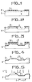
- the present invention relates to a method of manufacturing a photodetector device making it possible to avoid these drawbacks. More specifically, the device according to the invention comprises a network of elementary detectors produced in a semiconductor substrate (1), and, placed between the elementary detectors and on the substrate (1), a layer (5) of a material opaque to the incident radiation.
- a junction was made, for example by diffusion in a layer 2 of P-type impurities if the substrate is N-type.
- the second step of the method consists in delimiting, in the layer 2 and the substrate 1, junction zones separated from each other, which will constitute the elementary photodetectors.
- a photosensitive lacquer or resin 3 is deposited on layer 2 on the surfaces which will constitute the photodiodes after the etching step below.
- FIG. 2 represents the next step in which grooves 4 have been produced between the zones protected by the lacquer layer 3.
- the etching of these grooves can be done for example by chemical attack; it must extend to a depth greater than that of layer 2, in order to isolate the mesa diodes from each other.
- Such an etching penetrates slightly under layer 3, as shown in FIG. 2 (zone 41), over a distance which can be of the order of a few micrometers, depending on the well-known phenomenon of under-etching.
- a junction surface smaller than the area protected by layer 3, which forms an overhanging frame is obtained.
- a thin layer 5 is deposited, chosen to be opaque to the radiation to be detected.
- the deposition of this layer 5 is made on the entire device, preferably using a directional evaporator, constituted for example by a high vacuum enclosure having a source of evaporation of small dimensions. As shown in FIG. 3, a directional evaporator, constituted for example by a high vacuum enclosure having a source of evaporation of small dimensions.
- this thin layer which can be about 1 / 10th of a micrometer thick, breaks down at the level of each elementary photodetector into three parts: a part 51 which covers the layer 3; a part 52 which covers the bottom of the grooves 4, and finally a part 53 which extends the part 52 and goes up along the sides of the groove 4 until possibly slightly covering the junction zone, but without reaching the layer 3 because of the geometry in the overhanging frame thereof, this protective effect being more or less accentuated depending on whether the phenomenon of under-etching is itself more or less accentuated.
- this layer 5 is in an insulating material to prevent the junction from being short-circuited; this layer may for example consist of an insulator loaded with opaque particles.
- a method of producing a device as described above therefore makes it possible to have a photodetector array with high resolution and low diaphoty.
Landscapes
- Light Receiving Elements (AREA)
- Solid State Image Pick-Up Elements (AREA)
Applications Claiming Priority (2)
| Application Number | Priority Date | Filing Date | Title |
|---|---|---|---|
| FR7921903A FR2464563A1 (fr) | 1979-08-31 | 1979-08-31 | Dispositif photodetecteur a semi-conducteur et procede de fabrication, et analyseur d'image comportant un tel dispositif |
| FR7921903 | 1979-08-31 |
Publications (3)
| Publication Number | Publication Date |
|---|---|
| EP0024970A2 EP0024970A2 (fr) | 1981-03-11 |
| EP0024970A3 EP0024970A3 (en) | 1982-06-09 |
| EP0024970B1 true EP0024970B1 (fr) | 1984-03-28 |
Family
ID=9229271
Family Applications (1)
| Application Number | Title | Priority Date | Filing Date |
|---|---|---|---|
| EP80401158A Expired EP0024970B1 (fr) | 1979-08-31 | 1980-08-06 | Procédé de fabrication d'un dispositif photodétecteur à semiconducteur |
Country Status (4)
| Country | Link |
|---|---|
| EP (1) | EP0024970B1 (show.php) |
| JP (1) | JPS5636174A (show.php) |
| DE (1) | DE3067263D1 (show.php) |
| FR (1) | FR2464563A1 (show.php) |
Families Citing this family (7)
| Publication number | Priority date | Publication date | Assignee | Title |
|---|---|---|---|---|
| US4446372A (en) * | 1981-07-01 | 1984-05-01 | Honeywell Inc. | Detector cold shield |
| JPS6018070A (ja) * | 1983-07-11 | 1985-01-30 | Sharp Corp | 二次元画像読取素子 |
| FR2557371B1 (fr) * | 1983-12-27 | 1987-01-16 | Thomson Csf | Dispositif photosensible comportant entre les detecteurs des zones opaques au rayonnement a detecter, et procede de fabrication |
| GB2175442B (en) * | 1985-05-15 | 1989-05-24 | Stc Plc | Laser manufacture |
| DE3667226D1 (de) * | 1985-08-27 | 1990-01-04 | Siemens Ag | Fotoempfindliche anordnung auf der basis von a-si:h fuer bildsensoren. |
| JPH06122630A (ja) * | 1992-10-12 | 1994-05-06 | Taiyo Yakuhin Kogyo Kk | 安定な塩酸セフォチアム製剤 |
| FR2990562B1 (fr) * | 2012-05-09 | 2015-03-06 | Sagem Defense Securite | Procede de realisation d'un capteur infrarouge insb |
Family Cites Families (9)
| Publication number | Priority date | Publication date | Assignee | Title |
|---|---|---|---|---|
| FR1578110A (show.php) * | 1968-06-17 | 1969-08-14 | ||
| US3864818A (en) * | 1969-05-06 | 1975-02-11 | Philips Corp | Method of making a target for a camera tube with a mosaic of regions forming rectifying junctions |
| FR2080849A6 (show.php) * | 1970-02-06 | 1971-11-26 | Radiotechnique Compelec | |
| JPS4828187A (show.php) * | 1971-08-13 | 1973-04-13 | ||
| US3810796A (en) * | 1972-08-31 | 1974-05-14 | Texas Instruments Inc | Method of forming dielectrically isolated silicon diode array vidicon target |
| JPS4996686A (show.php) * | 1973-01-16 | 1974-09-12 | ||
| JPS569020B2 (show.php) * | 1974-03-20 | 1981-02-26 | ||
| JPS52131489A (en) * | 1976-04-28 | 1977-11-04 | Oki Electric Ind Co Ltd | Photoelectric converter |
| JPS5527657A (en) * | 1978-08-19 | 1980-02-27 | Fujitsu Ltd | Method of manufacturing infrared ray detecting element |
-
1979
- 1979-08-31 FR FR7921903A patent/FR2464563A1/fr active Granted
-
1980
- 1980-08-06 EP EP80401158A patent/EP0024970B1/fr not_active Expired
- 1980-08-06 DE DE8080401158T patent/DE3067263D1/de not_active Expired
- 1980-08-25 JP JP11605180A patent/JPS5636174A/ja active Pending
Also Published As
| Publication number | Publication date |
|---|---|
| DE3067263D1 (en) | 1984-05-03 |
| EP0024970A3 (en) | 1982-06-09 |
| FR2464563B1 (show.php) | 1981-09-11 |
| FR2464563A1 (fr) | 1981-03-06 |
| JPS5636174A (en) | 1981-04-09 |
| EP0024970A2 (fr) | 1981-03-11 |
Similar Documents
| Publication | Publication Date | Title |
|---|---|---|
| EP0350351B1 (fr) | Photodiode et matrice de photodiodes sur matériau II-VI et leurs procédés de fabrication | |
| EP2786105B1 (fr) | Detecteur infrarouge a base de micro-planches bolometriques suspendues | |
| EP0186225B1 (fr) | Capteur d'images pour caméra fonctionnant en mode "jour-nuit" | |
| EP1516368A2 (fr) | Imageur | |
| FR2954854A1 (fr) | Photodetecteur a structure plasmon | |
| EP2432034B1 (fr) | Détecteur bispectral multicouche à photodiodes et procédé de fabrication d'un tel détecteur | |
| EP1756872B1 (fr) | Circuit de detection photonique a structure mesa | |
| EP3012876A1 (fr) | Procede de fabrication d'une photodiode a faible bruit | |
| EP0024970B1 (fr) | Procédé de fabrication d'un dispositif photodétecteur à semiconducteur | |
| EP1903612B1 (fr) | Photodiode à avalanche | |
| EP0001728B1 (fr) | Diode émettrice et réceptrice de lumière notamment pour télécommunications optiques | |
| EP0229574B1 (fr) | Detecteur photovoltaique en HgCdTe a heterojonction et son procédé de fabrication | |
| EP2276072B1 (fr) | Element photodetecteur | |
| FR2683391A1 (fr) | Capteur d'images infrarouge. | |
| EP2432033A2 (fr) | Détecteur bispectral multicouche à photodiodes | |
| EP3582258B1 (fr) | Puce électronique protégée | |
| EP2415078B1 (fr) | Dispositif de detection d'image electronique | |
| FR2626109A1 (fr) | Dispositifs de visualisation de rayonnement thermique, systemes comportant de tels dispositifs, et methode de fabrication de tels dispositifs de visualisation | |
| EP3714243A1 (fr) | Dispositif de détection d'un rayonnement électromagnétique a diaphotie réduite | |
| FR3163770A1 (fr) | Dispositif électronique ayant des pixels à base de boîtes quantiques | |
| FR2771855A1 (fr) | Dispositif de photodetection, procede de fabrication de ce dispositif et application a la detection multispectrale | |
| FR3006105A1 (fr) | Matrice de photodiode a absorption reglable de charge | |
| FR2887076A1 (fr) | Capteur d'image a substrat semiconducteur aminci avec metallisation arriere | |
| FR3026562A1 (fr) | Detecteur infrarouge mulispectral. | |
| FR3092700A1 (fr) | Matrice de photo-détecteurs à barrière avec pixellisation par déplétions locales |
Legal Events
| Date | Code | Title | Description |
|---|---|---|---|
| PUAI | Public reference made under article 153(3) epc to a published international application that has entered the european phase |
Free format text: ORIGINAL CODE: 0009012 |
|
| AK | Designated contracting states |
Designated state(s): DE GB |
|
| PUAL | Search report despatched |
Free format text: ORIGINAL CODE: 0009013 |
|
| AK | Designated contracting states |
Designated state(s): DE GB |
|
| 17P | Request for examination filed |
Effective date: 19820623 |
|
| RBV | Designated contracting states (corrected) |
Designated state(s): DE GB |
|
| GRAA | (expected) grant |
Free format text: ORIGINAL CODE: 0009210 |
|
| AK | Designated contracting states |
Designated state(s): DE GB |
|
| REF | Corresponds to: |
Ref document number: 3067263 Country of ref document: DE Date of ref document: 19840503 |
|
| PLBE | No opposition filed within time limit |
Free format text: ORIGINAL CODE: 0009261 |
|
| STAA | Information on the status of an ep patent application or granted ep patent |
Free format text: STATUS: NO OPPOSITION FILED WITHIN TIME LIMIT |
|
| 26N | No opposition filed | ||
| PGFP | Annual fee paid to national office [announced via postgrant information from national office to epo] |
Ref country code: DE Payment date: 19920711 Year of fee payment: 13 |
|
| PGFP | Annual fee paid to national office [announced via postgrant information from national office to epo] |
Ref country code: GB Payment date: 19920717 Year of fee payment: 13 |
|
| PG25 | Lapsed in a contracting state [announced via postgrant information from national office to epo] |
Ref country code: GB Effective date: 19930806 |
|
| GBPC | Gb: european patent ceased through non-payment of renewal fee |
Effective date: 19930806 |
|
| PG25 | Lapsed in a contracting state [announced via postgrant information from national office to epo] |
Ref country code: DE Effective date: 19940503 |