EP0022968B2 - High capacitance multilayer bus bar and method of manufacture thereof - Google Patents
High capacitance multilayer bus bar and method of manufacture thereof Download PDFInfo
- Publication number
- EP0022968B2 EP0022968B2 EP80103840A EP80103840A EP0022968B2 EP 0022968 B2 EP0022968 B2 EP 0022968B2 EP 80103840 A EP80103840 A EP 80103840A EP 80103840 A EP80103840 A EP 80103840A EP 0022968 B2 EP0022968 B2 EP 0022968B2
- Authority
- EP
- European Patent Office
- Prior art keywords
- conductive
- chips
- bus bars
- adhesive
- bus bar
- Prior art date
- Legal status (The legal status is an assumption and is not a legal conclusion. Google has not performed a legal analysis and makes no representation as to the accuracy of the status listed.)
- Expired
Links
Images

Classifications
-
- H—ELECTRICITY
- H01—ELECTRIC ELEMENTS
- H01B—CABLES; CONDUCTORS; INSULATORS; SELECTION OF MATERIALS FOR THEIR CONDUCTIVE, INSULATING OR DIELECTRIC PROPERTIES
- H01B7/00—Insulated conductors or cables characterised by their form
- H01B7/0009—Details relating to the conductive cores
- H01B7/0018—Strip or foil conductors
-
- H—ELECTRICITY
- H02—GENERATION; CONVERSION OR DISTRIBUTION OF ELECTRIC POWER
- H02G—INSTALLATION OF ELECTRIC CABLES OR LINES, OR OF COMBINED OPTICAL AND ELECTRIC CABLES OR LINES
- H02G5/00—Installations of bus-bars
- H02G5/005—Laminated bus-bars
-
- H—ELECTRICITY
- H05—ELECTRIC TECHNIQUES NOT OTHERWISE PROVIDED FOR
- H05K—PRINTED CIRCUITS; CASINGS OR CONSTRUCTIONAL DETAILS OF ELECTRIC APPARATUS; MANUFACTURE OF ASSEMBLAGES OF ELECTRICAL COMPONENTS
- H05K1/00—Printed circuits
- H05K1/02—Details
- H05K1/0213—Electrical arrangements not otherwise provided for
- H05K1/0263—High current adaptations, e.g. printed high current conductors or using auxiliary non-printed means; Fine and coarse circuit patterns on one circuit board
-
- H—ELECTRICITY
- H05—ELECTRIC TECHNIQUES NOT OTHERWISE PROVIDED FOR
- H05K—PRINTED CIRCUITS; CASINGS OR CONSTRUCTIONAL DETAILS OF ELECTRIC APPARATUS; MANUFACTURE OF ASSEMBLAGES OF ELECTRICAL COMPONENTS
- H05K1/00—Printed circuits
- H05K1/16—Printed circuits incorporating printed electric components, e.g. printed resistors, capacitors or inductors
- H05K1/162—Printed circuits incorporating printed electric components, e.g. printed resistors, capacitors or inductors incorporating printed capacitors
-
- Y—GENERAL TAGGING OF NEW TECHNOLOGICAL DEVELOPMENTS; GENERAL TAGGING OF CROSS-SECTIONAL TECHNOLOGIES SPANNING OVER SEVERAL SECTIONS OF THE IPC; TECHNICAL SUBJECTS COVERED BY FORMER USPC CROSS-REFERENCE ART COLLECTIONS [XRACs] AND DIGESTS
- Y10—TECHNICAL SUBJECTS COVERED BY FORMER USPC
- Y10T—TECHNICAL SUBJECTS COVERED BY FORMER US CLASSIFICATION
- Y10T29/00—Metal working
- Y10T29/49—Method of mechanical manufacture
- Y10T29/49002—Electrical device making
- Y10T29/49117—Conductor or circuit manufacturing
- Y10T29/49124—On flat or curved insulated base, e.g., printed circuit, etc.
- Y10T29/49126—Assembling bases
Definitions
- This invention relates to multilayer bus bars, especially relatively small or miniature bus bars. More particularly, this invention relates to multilayer bus bar assemblies, and the method of manufacture thereof, wherein the bus bar assembly incorporates capacitive elements between layers of bus conductors to provide high capacitance bus bars.
- bus bars of relatively small or miniature size have been known in the art for a number of years. These devices are used for power and/or signal distribution in many systems, such as, for example, computer back panels and integrated circuit systems.
- Such prior art multilayer bus bars comprise at least two conductive plates (usually in the form of elongated strips of bars of copper) separated by an insulating film.
- a typical prior art bus bar of this type may use copper conductors having a thickness of about 0.25.mm, and the overall dimensions of the bus bar may be from about 0.48 mm to 3.05 mm thick, from about 3.8 mm to 5 mm wide and range in length up to 400 mm.
- the separating insulating layer is a plastic dielectric film such as the polyester material known under the registered Trade Mark MYLAR.
- the MYLAR separator layer and the conductive plates are bonded together by an adhesive.
- Prior art bus bars of this type have relatively low capacitance.
- a method has also been suggested (see GB-A-825 900) for interconnecting an aluminium terminal member to an aluminium capacitor foil member which comprises forming a brittle good dielectric oxide layer over the natural oxide layer.
- the purpose of the present invention is to provide a high capacitance multilayer bus car, and a method of manufacture thereof, which eliminate the need for the use of conductive adhesive, thereby completely eliminating the potential problems posed by the conductive adhesive in prior art devices.
- a multilayer bus bar including at least two spaced apart conductive elements having opposed inwardly facing surfaces, capacitive means positioned between said conductive elements, said capacitive means comprising a dielectric material between conductive outer surfaces, and further including an adhesive bonding said conductive elements to the outer surface of said capacitive means, characterized in that either the conductive outer surfaces of said capacitive means or the inwardly facing surfaces of said conductive elements are deliberately roughened so that a difference in roughness is established between said surfaces, and in that the degree of the deliberately established roughness and the amount of adhesive are such that electrical contact and a firm physical bond between each of said conductive outer surfaces of said capacitive means and the adjacent inwardly facing surfaces of the said conductive elements is established, in that the tops of the hills of the said deliberately roughened surfaces contact the adjacent other conductive surfaces, whereas the valleys between the hills of the deliberately roughened surfaces are filled with the adhesive, said adhesive being non conductive.
- a multilayer bus bar including first and second spaced apart generally flat conductive bus bars, said first and second bus bars having opposed inwardly facing surfaces having a first surface roughness, a plurality of generally flat capacitive chips between said first and second bus bars, said chips having a dielectric center between conductive outer surfaces of a second surface roughness, and further including an adhesive bonding said bus bars to part of the outer surface of said chips, characterized in that either the first or the second surface roughness is deliberately established so that said second surface roughness of said conductive surfaces of said chips is different from said first roughness of said bus bars and in that the degree of the deliberately established roughness and the amount of adhesive are such that electrical contact and a firm physical bond between each conductive outer surface of each capacitive chip and the adjacent inwardly facing surface of the bus bars is established, in that the tops of the hills of the said deliberately roughened surfaces contact the adjacent other conductive surfaces, whereas the valleys between the hills of the deliberately roughened surfaces are filled with the adhesive, said adhesive being non conductive.
- the invention also provides a process of forming a multilayer bus bar including the steps of forming a pair of generally flat conductive bus bars forming capacitive chips having a dielectric center between conductive outer surfaces, either the outer surfaces of said chips or the inwardly facing surfaces of said bus bars being deliberately roughened to provide the said difference of roughness of said surfaces, applying non conductive adhesive to inwardly facing surfaces of each bus bar, positioning said chips on a said inwardly facing surface of one of said bus bars, positioning the other of said bus bars on said chips to form a sandwich assembly of said chips between said bus bars, treating said assembly under heat and pressure to effect the said electrical contact and firm physical bond between said bus bars and chips.
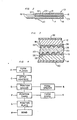
- a multilayer bus bar 10 has a first conductive plate 12 and a second conductive plate 14.
- Each of the plates 12 and 14 has a plurality of distribution prongs or tangs 16 extending therefrom, these tangs serving for electrical distribution and/or physical mounting of the bus bar on a printed circuit board or other structure.
- Conductive plates 12 and 14 are preferably tin plated copper elements approximately 0.25 mm thick and ranging in width from 3.8 mm to 5 mm and ranging in length from about 50 to 400 mm.
- the inwardly facing surfaces of plates 12 and 14 are coated with a coating 18 of nonconductive adhesive which flows freely when melted.
- the adhesive is preferably a thermoplastic polyester adhesive, such as Morton 76P1 (made by Morton Chemical Company Division of Mortion International Incorporated), which has low melt viscosity (on the order of about 100 cps) and flows freely at about 157 °C.
- the adhesive may be a thermosetting material if the cure thereof takes place during or after melting in manufacturing process.
- Capacitive elements are positioned between the inwardly opposing faces of plates 12 and 14.
- the capacitive elements are in the form of a plurality of ceramic dielectric chips 20 each having a relatively high dielectric constant.
- the ceramic dielectric chips have a thickness in the range from about 0.127 mm to about 0.38 mm and have a surface dimension in the range of from about 5 mm by 5 mm by to about 5 mm by 76 mm. Those surface dimensions represent the dimensions of opposed generally parallel plate surfaces of the chips.
- the ceramic material from which the chips are formed has a relatively high dielectric constant, preferably in excess of 8.000. Ceramic materials that are commonly used for capacitors may be used for the chips employed in the present invention.
- An exemplary and preferred ceramic material is barium titanite and modifications thereof.
- each of the chips 20 is coated on the opposed plate faces with a thin, intimate and continuous conductive coating 22 of metal, such as silver, or conductive polymer. It will be understood that although only one of each of the coated surfaces 22 is visible in Figure 1, the opposite parallel surface of each chip 20 will also be conductively coated. In effect, each chip 20 forms a small capacitor.
- An insulating separator layer or spacer 24 is also positioned between the conductive plates 12 and 14.
- the presence of spacer 24 is not absolutely required, but it is preferable to insure separation between conductive plates 12 and 14.
- Windows 25 are formed in spacer 24, and the chips 20 are positioned in windows 25. It will be understood that, depending on the size of the chips 20, several of the chips may be located in each window 25.
- spacer 24 also promotes parallel contact between the surface of the plates 12 and 14 and the opposed conductive surfaces 22 of the capacitive chips, thereby enhancing the capacitive capabilities of the assembly.
- Plates 12 and 14 are formed, such as by die stamping, in step A, and spacer 24 is formed in a separate step B, also such as by die stamping.
- the adhesive 18 is then applied to the inwardly facing surfaces of plates 12 and 14 in step C.
- the adhesive is preferably in the form of a liquid which can be applied in any convenient fashion such as painting, spraying, roll coating, etc.
- spacer 24 is placed on the inwardly facing surface of one of the plates 12 or 14.
- the capacitive chips 20 (which are formed in Step E) are then placed in the window 26 of spacer 24 in step F so that one of the flat plate surfaces of each chip is in contact with the inwardly facing surface of the plate 12 or 14 on which the separator has been placed.
- the second plate is then positioned over the spacer and chips in step G so as to form a sandwich with the spacer 24 and chips 20 sandwiched between the plates 12 and 14.
- This sandwich assembly is positioned on a first outer layer of MYLAR insulation 30 and is covered with a second outer layer of MYLAR insulation 32. Insulation layers 30 and 32 are slightly larger than the bodies of plates 12 and 14 so that they can be wrapped around the edges of and encapsulate the sandwich assembly of plates 12 and 14 and chips 20.
- step H The inwardly facing surfaces of insulation layers 30 and 32 are also coated with non-conductive adhesive so as to bond, respectively the outer surfaces of plates 12 and 14.
- This entire assembly is then bonded under heat and pressure in step H to form an integral encapsulated assembly. Bonding occurs at a temperature of from about 150°C to about 178°C and at a pressure of from about 3,5 kg/cm 2 to about 14 kg/cm 2 , the heat and pressure being applied for a period of from about 5 minutes to about 60 minutes. The pressure is distributed evenly across the entire assembly so that when the adhesive melts excess adhesive is squeezed out of the assembly, whereby physical and electrical contact is established between the outer plates 12 and 14 and the conductive surfaces of the chips, as will be explained in more detail hereinafter. Bonding under heated pressure is accomplished in a press, and the permissible pressure is limited only by the compressive strength of the capacitive chips.
- the encapsulation of the conductive plates 12 and 14 by outer sheets 30 and 32 is preferable but not necessary. Furthermore, if the plates are to be encapsulated, any other method of encapsulation known in the art can be used.
- the adhesive since the adhesive is nonconductive, the adhesive can be permitted to flow in the assembly and actually flow between the conductive plates 12 and 14. This not only enhances bonding, but it also permits the parts to be squeezed together to squeeze out excess adhesive whereby a thinner sandwich structure can be achieved.
- the opposed plate surfaces of the chips are formed so that they are deliberately roughened or coarse and nonporous so that the plate surfaces of the chips are coarser than the inwardly facing surfaces of the conductive plates 12 and 14 to which the chips and bonded.
- the roughness or coarseness of the plate surfaces of the chips is on the order of 7.62 microns or more. That is, the plate surfaces of the chips, although flat and parallel on a microscopic basis, have, on a microscopic basis, hills 26 and valleys 28 where the distance between the top of the hill and the bottom of the valley is on the order of 7.62 microns or more.
- a preferred dielectric material for chips 20 is barium titanite.
- the plate surfaces of the chips can be roughened in several ways.
- zirconium oxide can be mixed with the barium titanite during the process of forming the chips. Because of the higher melting point of the zirconium oxide (i. e. higher than barium titanite) the zirconium oxide does not melt during the firing process of chip formation. Rather, the zirconium oxide remains in its particle solid state and forms roughened plate surfaces on the opposite plate surfaces of the chip.
- the chips are then coated with a thin coating of silver or other conductive material, and the thin conductive coating conforms to the roughened surfaces of the base material of the chips thereby retaining the coarseness or roughness of the chip surfaces.
- the roughned surfaces can be formed by mixing particles of a ceramic material, such as barium titanite, for example, with the conductive coating to be applied to the chips. These particles of ceramic material in the conductive coating will serve to form the roughened surface of the opposed plate surfaces of the chips.
- a ceramic material such as barium titanite
- the plate surfaces of the chips can be retained relatively smooth, and the inwardly facing surfaces of the conductors 12 and 14 can be roughened, such as by sand paper, coining the dye from which they are formed, etc.
- the same end result will be obtained : i. e., there will be direct physical and electrical contact between the hills - on the roughened inner surfaces of the plate conductors 12 and 14 and the relatively smooth plate surfaces of the chips, while adhesive bonding will be achieved across the adhesive retained between the « valleys on the inner surfaces of the conductors 12 and 14 and the chips.
- the essential feature is to deliberately establish a certain surface roughness or coarseness (on the order of 7.62 microns or more) on the plate surfaces of the chips or on the inwardly facing surfaces of the conductors 12 and 14.
- This differential roughness or coarseness insures that there will be direct physical and electrical contact between parts of each chip and the conductors while also retaining adhesive between other parts thereof to accomplish adhesive bonding.
Landscapes
- Fixed Capacitors And Capacitor Manufacturing Machines (AREA)
- Insulated Conductors (AREA)
Applications Claiming Priority (2)
| Application Number | Priority Date | Filing Date | Title |
|---|---|---|---|
| US06/059,068 US4236038A (en) | 1979-07-19 | 1979-07-19 | High capacitance multilayer bus bar and method of manufacture thereof |
| US59068 | 1979-07-19 |
Publications (3)
| Publication Number | Publication Date |
|---|---|
| EP0022968A1 EP0022968A1 (en) | 1981-01-28 |
| EP0022968B1 EP0022968B1 (en) | 1983-12-21 |
| EP0022968B2 true EP0022968B2 (en) | 1988-11-30 |
Family
ID=22020638
Family Applications (1)
| Application Number | Title | Priority Date | Filing Date |
|---|---|---|---|
| EP80103840A Expired EP0022968B2 (en) | 1979-07-19 | 1980-07-05 | High capacitance multilayer bus bar and method of manufacture thereof |
Country Status (6)
| Country | Link |
|---|---|
| US (1) | US4236038A (https=) |
| EP (1) | EP0022968B2 (https=) |
| JP (1) | JPS5618309A (https=) |
| BR (1) | BR8004522A (https=) |
| CA (1) | CA1146641A (https=) |
| DE (1) | DE3065941D1 (https=) |
Families Citing this family (36)
| Publication number | Priority date | Publication date | Assignee | Title |
|---|---|---|---|---|
| US4346257A (en) * | 1980-03-18 | 1982-08-24 | Eldre Components, Inc. | Laminated bus bar with dielectric ceramic inserts |
| US4343965A (en) * | 1980-04-14 | 1982-08-10 | Bussco Engineering, Inc. | Bus bar assembly |
| FR2495388A1 (fr) * | 1980-11-28 | 1982-06-04 | Europ Composants Electron | Barre d'alimentation comportant un empilement de 2 n + 2 couches metalliques separees par 2 n + 1 couches dielectriques |
| US4436953A (en) * | 1981-03-31 | 1984-03-13 | Rogers Corporation | Bus bar assembly with discrete capacitor elements |
| US4381423A (en) * | 1981-03-31 | 1983-04-26 | Rogers Corporation | High capacitance bus bar manufacturing technique |
| US4401843A (en) * | 1981-03-31 | 1983-08-30 | Rogers Corporation | Miniaturized bus bars and methods of fabrication thereof |
| US4403108A (en) * | 1981-03-31 | 1983-09-06 | Rogers Corporation | Miniaturized bus bar with capacitors and assembly technique |
| US4440972A (en) * | 1981-03-31 | 1984-04-03 | Rogers Corporation | Miniaturized bus bar with capacitors and method of making same |
| US4451694A (en) * | 1981-03-31 | 1984-05-29 | Rogers Corporation | Miniaturized high capacitance bus bar assembly |
| JPS581915A (ja) * | 1981-06-27 | 1983-01-07 | 日本メクトロン株式会社 | ハイキヤパシタンス積層母線 |
| JPS58142708A (ja) * | 1982-02-18 | 1983-08-24 | エルドレ コ−ポネンツ インコ−ポレ−シヨン | 絶縁セラミック插入物を用いた積層バスバ−とその製造方法 |
| DE3205819A1 (de) * | 1982-02-18 | 1983-08-25 | Eldre Components, Inc., 14623 Rochester, N.Y. | Verfahren zur herstellung einer schichtweise aufgebauten sammelschiene mit hoher kapazitaet |
| US4429344A (en) * | 1982-05-14 | 1984-01-31 | Sangamo Weston, Inc. | Conductive foils for solid dielectric capacitor |
| US4430522A (en) * | 1982-07-16 | 1984-02-07 | Eldre Components, Inc. | Laminated bus bar with capacitors and method of making same |
| IT1194301B (it) * | 1983-07-06 | 1988-09-14 | Mecondor Spa | Metodo per la fabbricazioni ad alta capacita' con connessioni elettriche ottenute per la saldatura,e relative barre prodotte secondo tale metodo |
| US4491895A (en) * | 1983-11-14 | 1985-01-01 | Rogers Corporation | Decoupling capacitor and method of manufacture thereof |
| US4494169A (en) * | 1983-11-14 | 1985-01-15 | Rogers Corporation | Decoupling capacitor and method of manufacture thereof |
| US4499519A (en) * | 1983-11-14 | 1985-02-12 | Rogers Corporation | Decoupling capacitor and method of manufacture thereof |
| US4497012A (en) * | 1983-11-14 | 1985-01-29 | Rogers Corporation | Decoupling capacitor and method of manufacture thereof |
| US4511951A (en) * | 1983-11-14 | 1985-04-16 | Rogers Corporation | Multilayer decoupling capacitor and method of manufacture thereof |
| US4594641A (en) * | 1985-05-03 | 1986-06-10 | Rogers Corporation | Decoupling capacitor and method of formation thereof |
| US4599486A (en) * | 1985-09-06 | 1986-07-08 | Rogers Corporation | High capacitance bus bar including multilayer ceramic capacitors |
| US4834673A (en) * | 1987-05-14 | 1989-05-30 | Amp Incorporated | Flat cable power distribution system |
| US4867696A (en) * | 1988-07-15 | 1989-09-19 | Amp Incorporated | Laminated bus bar with power tabs |
| US5107393A (en) * | 1990-11-28 | 1992-04-21 | Magnetek Universal Manufacturing | Metallized film capacitor construction |
| US5185690A (en) * | 1991-10-16 | 1993-02-09 | Miller Mark L | High dielectric constant sheet material |
| JP3510024B2 (ja) * | 1995-11-02 | 2004-03-22 | 矢崎総業株式会社 | 平面回路体の端末接続部およびその製造方法 |
| DE29912703U1 (de) * | 1999-07-19 | 1999-11-11 | Siemens AG, 80333 München | Überspannungsableiter |
| CA2350191A1 (en) * | 2001-06-12 | 2002-12-12 | Fci Canada Inc. | Bus bar with frequency-filtering geometry |
| US7307022B2 (en) * | 2004-11-19 | 2007-12-11 | Endicott Interconnect Technologies, Inc. | Method of treating conductive layer for use in a circuitized substrate and method of making said substrate having said conductive layer as part thereof |
| EP2264726B1 (de) | 2005-05-02 | 2014-09-10 | Epcos Ag | Kondensator |
| EP2306477B1 (de) | 2005-05-02 | 2013-07-03 | Epcos AG | Leistungskondensator |
| JP4905254B2 (ja) * | 2007-05-25 | 2012-03-28 | トヨタ自動車株式会社 | コンデンサ一体バスバーの製造方法 |
| US10998706B2 (en) * | 2019-10-08 | 2021-05-04 | Hamilton Sundstrand Corporation | Laminated bus bars |
| CN116505348A (zh) * | 2022-12-21 | 2023-07-28 | 北京卫星制造厂有限公司 | 一种汇流片的设计与装联方法 |
| US20260096048A1 (en) * | 2024-10-01 | 2026-04-02 | Nvidia Corporation | Data center apparatus for electrical energy storage |
Family Cites Families (10)
| Publication number | Priority date | Publication date | Assignee | Title |
|---|---|---|---|---|
| US1999137A (en) * | 1926-08-10 | 1935-04-23 | Frank L Walker | Radio apparatus |
| US2615946A (en) * | 1948-07-16 | 1952-10-28 | Katzman Jacob | Flat terminal element for condenser foil |
| GB825900A (en) * | 1956-10-15 | 1959-12-23 | Gen Motors Corp | Improvements in or relating to a method of interconnecting an aluminium terminal member to an aluminium capacitor foil member |
| US3396230A (en) * | 1966-07-06 | 1968-08-06 | Thomas & Betts Corp | Laminated bus assemblies |
| FR1539677A (fr) * | 1967-05-18 | 1968-09-20 | Comp Generale Electricite | Structure de condensateur et application aux lignes capacitives |
| DE2112236A1 (de) * | 1971-03-13 | 1972-09-14 | Licentia Gmbh | Verfahren zur Herstellung von keramischen Bauelementen |
| FR2138403B1 (https=) * | 1971-05-25 | 1976-12-03 | Europ Composants Electron | |
| US3886654A (en) * | 1974-01-22 | 1975-06-03 | Eldre Components | Method of manufacturing laminated bus bars |
| US4114120A (en) * | 1976-11-23 | 1978-09-12 | Dielectric Laboratories, Inc. | Stripline capacitor |
| JPS6021451B2 (ja) * | 1977-10-08 | 1985-05-28 | 日本メクトロン株式会社 | コンデンサ内蔵型積層母線 |
-
1979
- 1979-07-19 US US06/059,068 patent/US4236038A/en not_active Expired - Lifetime
-
1980
- 1980-06-18 CA CA000354242A patent/CA1146641A/en not_active Expired
- 1980-07-05 DE DE8080103840T patent/DE3065941D1/de not_active Expired
- 1980-07-05 EP EP80103840A patent/EP0022968B2/en not_active Expired
- 1980-07-16 JP JP9816080A patent/JPS5618309A/ja active Granted
- 1980-07-17 BR BR8004522A patent/BR8004522A/pt not_active IP Right Cessation
Also Published As
| Publication number | Publication date |
|---|---|
| JPH0114644B2 (https=) | 1989-03-13 |
| JPS5618309A (en) | 1981-02-21 |
| US4236038A (en) | 1980-11-25 |
| EP0022968A1 (en) | 1981-01-28 |
| BR8004522A (pt) | 1981-02-03 |
| EP0022968B1 (en) | 1983-12-21 |
| DE3065941D1 (en) | 1984-01-26 |
| CA1146641A (en) | 1983-05-17 |
Similar Documents
| Publication | Publication Date | Title |
|---|---|---|
| EP0022968B2 (en) | High capacitance multilayer bus bar and method of manufacture thereof | |
| US4382156A (en) | Multilayer bus bar fabrication technique | |
| EP0398811B1 (en) | Manufacturing method for a PTC thermistor | |
| CA1127254A (en) | High capacitance bus bar | |
| US4584768A (en) | Method of making high capacitive multilayer conductive bars | |
| MY113149A (en) | Method of manufacturing a printed circuit assembly | |
| US4436953A (en) | Bus bar assembly with discrete capacitor elements | |
| US4430522A (en) | Laminated bus bar with capacitors and method of making same | |
| US4401843A (en) | Miniaturized bus bars and methods of fabrication thereof | |
| US4599486A (en) | High capacitance bus bar including multilayer ceramic capacitors | |
| US4399321A (en) | High capacitance bus bar including multilayer ceramic capacitors | |
| US4440972A (en) | Miniaturized bus bar with capacitors and method of making same | |
| US4451694A (en) | Miniaturized high capacitance bus bar assembly | |
| US4394532A (en) | Multilayer current distribution systems and methods of fabrication thereof | |
| US5440802A (en) | Method of making wire element ceramic chip fuses | |
| US4618911A (en) | End termination for chip capacitor | |
| US4342881A (en) | Laminated bus bar and method of manufacture | |
| US4685026A (en) | Capacitor forming and manufacturing method | |
| JPS6110203A (ja) | 有機正特性サ−ミスタ | |
| CA1181498A (en) | Miniaturized bus bar and assembly technique | |
| US4429344A (en) | Conductive foils for solid dielectric capacitor | |
| US4420653A (en) | High capacitance bus bar and method of manufacture thereof | |
| JPH0335583A (ja) | フレキシブル回路基板及びそのスルーホール部の形成方法 | |
| GB2054267A (en) | High capacitance bus bar | |
| GB2115213A (en) | Laminated bus bar with dielectric inserts |
Legal Events
| Date | Code | Title | Description |
|---|---|---|---|
| PUAI | Public reference made under article 153(3) epc to a published international application that has entered the european phase |
Free format text: ORIGINAL CODE: 0009012 |
|
| AK | Designated contracting states |
Designated state(s): BE DE FR GB IT NL SE |
|
| 17P | Request for examination filed |
Effective date: 19810703 |
|
| ITF | It: translation for a ep patent filed | ||
| GRAA | (expected) grant |
Free format text: ORIGINAL CODE: 0009210 |
|
| AK | Designated contracting states |
Designated state(s): BE DE FR GB IT NL SE |
|
| REF | Corresponds to: |
Ref document number: 3065941 Country of ref document: DE Date of ref document: 19840126 |
|
| ET | Fr: translation filed | ||
| PLBI | Opposition filed |
Free format text: ORIGINAL CODE: 0009260 |
|
| 26 | Opposition filed |
Opponent name: TECO S.A. Effective date: 19840919 |
|
| BECN | Be: change of holder's name |
Effective date: 19861128 |
|
| ITPR | It: changes in ownership of a european patent |
Owner name: CESSIONE;MEKTRON N.V. |
|
| REG | Reference to a national code |
Ref country code: FR Ref legal event code: TP |
|
| NLS | Nl: assignments of ep-patents |
Owner name: MEKTRON N.V. TE GENT, BELGIE. |
|
| RAP2 | Party data changed (patent owner data changed or rights of a patent transferred) |
Owner name: MEKTRON N.V. |
|
| REG | Reference to a national code |
Ref country code: GB Ref legal event code: 732 |
|
| PUAH | Patent maintained in amended form |
Free format text: ORIGINAL CODE: 0009272 |
|
| STAA | Information on the status of an ep patent application or granted ep patent |
Free format text: STATUS: PATENT MAINTAINED AS AMENDED |
|
| 27A | Patent maintained in amended form |
Effective date: 19881130 |
|
| AK | Designated contracting states |
Kind code of ref document: B2 Designated state(s): BE DE FR GB IT NL SE |
|
| NLR2 | Nl: decision of opposition | ||
| ET3 | Fr: translation filed ** decision concerning opposition | ||
| NLR3 | Nl: receipt of modified translations in the netherlands language after an opposition procedure | ||
| ITF | It: translation for a ep patent filed | ||
| PGFP | Annual fee paid to national office [announced via postgrant information from national office to epo] |
Ref country code: SE Payment date: 19900625 Year of fee payment: 11 Ref country code: BE Payment date: 19900625 Year of fee payment: 11 |
|
| ITTA | It: last paid annual fee | ||
| PGFP | Annual fee paid to national office [announced via postgrant information from national office to epo] |
Ref country code: NL Payment date: 19900731 Year of fee payment: 11 |
|
| PG25 | Lapsed in a contracting state [announced via postgrant information from national office to epo] |
Ref country code: SE Effective date: 19910706 |
|
| PG25 | Lapsed in a contracting state [announced via postgrant information from national office to epo] |
Ref country code: BE Effective date: 19910731 |
|
| BERE | Be: lapsed |
Owner name: MEKTRON N.V. Effective date: 19910731 |
|
| PG25 | Lapsed in a contracting state [announced via postgrant information from national office to epo] |
Ref country code: NL Effective date: 19920201 |
|
| NLV4 | Nl: lapsed or anulled due to non-payment of the annual fee | ||
| REG | Reference to a national code |
Ref country code: GB Ref legal event code: 732E |
|
| PGFP | Annual fee paid to national office [announced via postgrant information from national office to epo] |
Ref country code: FR Payment date: 19930610 Year of fee payment: 14 |
|
| PGFP | Annual fee paid to national office [announced via postgrant information from national office to epo] |
Ref country code: DE Payment date: 19930618 Year of fee payment: 14 |
|
| PGFP | Annual fee paid to national office [announced via postgrant information from national office to epo] |
Ref country code: GB Payment date: 19930624 Year of fee payment: 14 |
|
| REG | Reference to a national code |
Ref country code: FR Ref legal event code: TP |
|
| ITPR | It: changes in ownership of a european patent |
Owner name: CESSIONE;CIRCUIT COMPONENTS INCORPORATED |
|
| PG25 | Lapsed in a contracting state [announced via postgrant information from national office to epo] |
Ref country code: GB Effective date: 19940705 |
|
| EUG | Se: european patent has lapsed |
Ref document number: 80103840.7 Effective date: 19920210 |
|
| GBPC | Gb: european patent ceased through non-payment of renewal fee |
Effective date: 19940705 |
|
| PG25 | Lapsed in a contracting state [announced via postgrant information from national office to epo] |
Ref country code: FR Effective date: 19950331 |
|
| REG | Reference to a national code |
Ref country code: FR Ref legal event code: ST |
|
| PG25 | Lapsed in a contracting state [announced via postgrant information from national office to epo] |
Ref country code: DE Effective date: 19951101 |