EP0020175B1 - Festkörper-Bildaufnahmevorrichtung - Google Patents
Festkörper-Bildaufnahmevorrichtung Download PDFInfo
- Publication number
- EP0020175B1 EP0020175B1 EP80301842A EP80301842A EP0020175B1 EP 0020175 B1 EP0020175 B1 EP 0020175B1 EP 80301842 A EP80301842 A EP 80301842A EP 80301842 A EP80301842 A EP 80301842A EP 0020175 B1 EP0020175 B1 EP 0020175B1
- Authority
- EP
- European Patent Office
- Prior art keywords
- solid
- imaging device
- state imaging
- film
- photoconductive film
- Prior art date
- Legal status (The legal status is an assumption and is not a legal conclusion. Google has not performed a legal analysis and makes no representation as to the accuracy of the status listed.)
- Expired
Links
- 238000003384 imaging method Methods 0.000 title claims description 32
- 239000000758 substrate Substances 0.000 claims description 10
- 239000004065 semiconductor Substances 0.000 claims description 9
- 239000000969 carrier Substances 0.000 claims description 8
- 230000005669 field effect Effects 0.000 claims description 3
- 238000006243 chemical reaction Methods 0.000 description 13
- 239000012535 impurity Substances 0.000 description 8
- 230000003287 optical effect Effects 0.000 description 7
- 230000035945 sensitivity Effects 0.000 description 5
- 229910021420 polycrystalline silicon Inorganic materials 0.000 description 4
- 238000001704 evaporation Methods 0.000 description 3
- 230000008020 evaporation Effects 0.000 description 3
- 239000000463 material Substances 0.000 description 3
- 206010034972 Photosensitivity reaction Diseases 0.000 description 2
- 229910021417 amorphous silicon Inorganic materials 0.000 description 2
- 239000000470 constituent Substances 0.000 description 2
- 230000005684 electric field Effects 0.000 description 2
- 238000010894 electron beam technology Methods 0.000 description 2
- 230000010354 integration Effects 0.000 description 2
- 230000036211 photosensitivity Effects 0.000 description 2
- 238000002360 preparation method Methods 0.000 description 2
- UFHFLCQGNIYNRP-UHFFFAOYSA-N Hydrogen Chemical compound [H][H] UFHFLCQGNIYNRP-UHFFFAOYSA-N 0.000 description 1
- XUIMIQQOPSSXEZ-UHFFFAOYSA-N Silicon Chemical compound [Si] XUIMIQQOPSSXEZ-UHFFFAOYSA-N 0.000 description 1
- 238000010521 absorption reaction Methods 0.000 description 1
- 238000010276 construction Methods 0.000 description 1
- 238000010586 diagram Methods 0.000 description 1
- 238000009826 distribution Methods 0.000 description 1
- 230000002349 favourable effect Effects 0.000 description 1
- 229910052739 hydrogen Inorganic materials 0.000 description 1
- 239000001257 hydrogen Substances 0.000 description 1
- 238000004519 manufacturing process Methods 0.000 description 1
- 238000000034 method Methods 0.000 description 1
- 238000005215 recombination Methods 0.000 description 1
- 230000006798 recombination Effects 0.000 description 1
- 229910052710 silicon Inorganic materials 0.000 description 1
- 239000010703 silicon Substances 0.000 description 1
- 238000009751 slip forming Methods 0.000 description 1
- 238000003860 storage Methods 0.000 description 1
- 238000007738 vacuum evaporation Methods 0.000 description 1
Images
Classifications
-
- H—ELECTRICITY
- H10—SEMICONDUCTOR DEVICES; ELECTRIC SOLID-STATE DEVICES NOT OTHERWISE PROVIDED FOR
- H10F—INORGANIC SEMICONDUCTOR DEVICES SENSITIVE TO INFRARED RADIATION, LIGHT, ELECTROMAGNETIC RADIATION OF SHORTER WAVELENGTH OR CORPUSCULAR RADIATION
- H10F39/00—Integrated devices, or assemblies of multiple devices, comprising at least one element covered by group H10F30/00, e.g. radiation detectors comprising photodiode arrays
- H10F39/10—Integrated devices
- H10F39/12—Image sensors
- H10F39/191—Photoconductor image sensors
Definitions
- This invention relates to a solid-state image pickup device for use in a television camera etc. Particularly it relates to a solid-state imaging deviced which has a photoelectric conversion layer, a plurality of switching elements and horizontal and vertical scanning circuits, all these constituents being provided in a major surface portion of a semiconductor body.
- a solid-state device which has a photoconductor and switching elements addressed by scanning circuits for reading out from the photoconductor optical information stored therein.
- Solid-state imaging devices are classified into two types; the type wherein optical signals are stored in photodiodes or MOS (Metal-Oxide-Semiconductor) capacitances formed on a semiconductor substrate, and the type wherein only scanning circuits (scanners) and groups of switches connected thereto are arrayed on a semiconductor substrate and they are overlaid with a photoconductive film for the function of photoelectric conversion.
- the former is such that scanning circuits, groups of switches for addressing and the photoelectric conversion elements are integrated, in general, on an identical plane and that the source junctions, for example, of insulated-gate field effect transistors (hereinbelow, termed "MOSTs”) serving as the switches can be utilized also for photoelectric conversion elements, so it can be fabricated comparatively easily.
- MOSTs insulated-gate field effect transistors
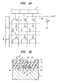
- FIG. 1A designates a horizontal scanner for turning "on” and “off” horizontal switching elements 3
- numeral 2 a vertical scanner for turning "on” and “off” vertical switching elements 4
- numeral 5 a photoelectric conversion part utilizing a photoconductive film
- numeral 6 a power supply input terminal for driving the photoelectric conversion parts 5
- numeral 10 a signal output line
- letter R a resistor
- Figure 1 B shows the sectional structure of the photoelectric conversion part and the switching elements in Figure 1A.
- Symbol 5' indicates the photoconductive film
- symbol 6' the power supply input terminal disposed through a transparent electrode 7
- symbol 3' the horizontal switching MOST
- symbol 4' the vertical switching MOST
- numeral 8 an insulating film.
- Numeral 11 denotes a semiconductor substrate, numerals 121 and 122 gate electrodes, and numeral 13 an electrode (of, for example, A1) which is held in ohmic contact with one end 91 of the switching MOST 4'.
- the resistance of the photoconductive film varies in accordance with the light intensity of the optical image, a signal voltage corresponding to the optical image appears at the one end 91 of the vertical switching MOST 4 (4'), and the variation is derived from an output terminal OUT through the signal output line 10 as a video signal.
- the inventors fabricated the aforecited solid-state imaging device by the use of the P-channel MOS device for fabricating technique which is the stablest in the MOS-IC tech- .nology, and evaluated its characteristics. More specifically, scanning circuits and groups of switches were constructed of P-channel MOSTs whose sources and drains were formed by diffusing P-type impurities into a Si substrate of the N-type conductivity, a Se-As-Te evaporation film which is used as the photoconductive film of an image pickup tube was disposed on the group of switches, and a transparent electrode was formed on the evaporated film (refer to U.S. Patents 3890525 and 4040985).
- the Se-As-Te film has a component distribution in the direction perpendicular to the plane of the film, and contains Se 50% or more as its component ratio within the film.
- the Se-As-Te amorphous film can be evaporated at the normal temperature, and is desirable for the solid-state imaging device requiring a long lifetime because the film after the fabrication is stabler than the other photoconductive films even in the air.
- the mobility of holes is greater than that of electrons, the predominant conduction charges are the holes, and the main constituents of current are the holes.
- the holes generated in the upper surface of the photoconductive film are mostly attracted to the transparent electrode 7 to which a minus voltage is applied, whereas the electrons scarcely reach the switch side electrode 13.
- the voltage variation on which the video signal is based does not arise in the switch side electrode 13, in other words, the photosensitivity is conspicuously low (since the P-channel MOST is operated by a minus voltage, the voltage variation owing to the storage of the electrons needs to appear in the switch side electrode).
- the sensitivity is the most important factor that determines the quality of the imaging device, and is a problem which must be solved by all means in order to realize household cameras, which are the main use of the solid-state imaging devices.
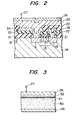
- a solid-stage imaging device comprising a semiconductor integrated circuit in which a plurality of switching elements for addressing positions of picture elements are disposed on a substrate, a photoconductive film which is disposed on the integrated circuit and which is connected with the respective switching elements, a light transmitting electrode which is disposed on the photoconductive film, and means for applying a voltage to the light transmitting electrode thereby to bias a region of the photoconductive film on a light entrance side either positively or negatively with respect to a region thereof on the opposite side; characterised in that each said switching element is an element which uses carriers of a polarity opposite to that of carriers having a greater mobility that that of the opposite polarity carriers in said photoconductive film.
- the switching elements are constructed of N-channel MOSTs; whereas in the case where the predominant conduction charges are electrons (N-type), the switching elements are constructed of P-channel MOSTs.
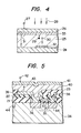
- Figure 4 is a view for explaining the operation of the imaging device, showing a detail of the photoconductive film and the vicinity thereof in Figures 2 and 3.
- excited charges or electrons 29 and holes 30 appear in various positions within the film.
- the predominant conduction charges are the holes of greater mobility, and the holes travel towards the electrode 24 efficiently (without disappearing midway due to recombination etc).
- the holes having been stored over one frame period are read out as a signal through the switching MOST 15 and a horizontal switching MOST and become a video signal.
- the holes on the electrode 24 disappear, so that the electrode 24 is cleared from a plus voltage to, for example, zero V to make preparations for the entrance of the optical image of the next frame.
- Short- wavelength light of high absorption efficiency (blue light) is mostly absorbed by an upper region 33 of the photoconductive film, but the holes generated in this region travel efficiently and are stored on the electrode 24. Therefore, the uncertainty of the blue sensitivity which is a problem in conventional silicon solid-state imaging devices can be remarkably improved.
- the sensitivities to green and red are high, and the sensitivity to the whole light or white light can be greatly improved. Accordingly, the above solid-state imaging device is an image pickup device which is favourable both for color image pickup and for black-and- white image pickup.
- the solid-state imaging device in Figure 2 was manufactured in accordance with a prior-art MOSIC processing step (Japanese Patent Application Laid-open Specification No. 53-122316, equivalent U.S. Patent 4148048) and a prior-art evaporation processing step for pickup tubes (Japanese Patent Application Publication Specification No. 52-30091, Japanese Patent Application Laid-open Specification No. 51-120611, equivalent U.S.
- Patent 4040985 in such a way that switching MOSTs 15 each consisting of N-type source and drain regions 16 and 19 at an impurity concentration of 10 19 ⁇ 10 21 /cm 3 and an N-type polycrystalline Si (impurity concentration 10' 9- 10 2 '/cm 3 ) gate electrode were disposed on a P-type Si substrate 14 at an impurity concentration of 4 ⁇ 8 ⁇ 10 14 /cm 3 , that AI layers being 5000 ⁇ -1 J im thick were used as an electrode 24 and a signal line 18, that a Se-As-Te amorphous evaporation film being 5000 ⁇ -5 ⁇ m thick was used as a photoconductive film 25, and that a Sn0 2 layering 1000 A-2 pm thick was used as an electrode 26. Then, a good device could be obtained.
- CCDs charge transfer devices
- this invention has the great advantage that, not only the enhancement of the sensitivity of the imaging device is realised, but also the use of materials in which the conduction is dominated by electrons and which have not heretofore been employed in practice is permitted.
- the industrial value of the invention is very great.
Landscapes
- Solid State Image Pick-Up Elements (AREA)
- Transforming Light Signals Into Electric Signals (AREA)
Claims (7)
Applications Claiming Priority (2)
| Application Number | Priority Date | Filing Date | Title |
|---|---|---|---|
| JP54068970A JPS6033342B2 (ja) | 1979-06-04 | 1979-06-04 | 固体撮像装置 |
| JP68970/79 | 1979-06-04 |
Publications (4)
| Publication Number | Publication Date |
|---|---|
| EP0020175A2 EP0020175A2 (de) | 1980-12-10 |
| EP0020175A3 EP0020175A3 (en) | 1981-04-01 |
| EP0020175B1 true EP0020175B1 (de) | 1983-05-18 |
| EP0020175B2 EP0020175B2 (de) | 1985-12-04 |
Family
ID=13389030
Family Applications (1)
| Application Number | Title | Priority Date | Filing Date |
|---|---|---|---|
| EP80301842A Expired EP0020175B2 (de) | 1979-06-04 | 1980-06-03 | Festkörper-Bildaufnahmevorrichtung |
Country Status (5)
| Country | Link |
|---|---|
| US (1) | US4323912A (de) |
| EP (1) | EP0020175B2 (de) |
| JP (1) | JPS6033342B2 (de) |
| CA (1) | CA1135821A (de) |
| DE (1) | DE3063289D1 (de) |
Families Citing this family (20)
| Publication number | Priority date | Publication date | Assignee | Title |
|---|---|---|---|---|
| JPS5689174A (en) * | 1979-12-21 | 1981-07-20 | Toshiba Corp | Solid image pickup device |
| JPS5772370A (en) * | 1980-10-23 | 1982-05-06 | Canon Inc | Photoelectric converter |
| US4571626A (en) * | 1981-09-17 | 1986-02-18 | Matsushita Electric Industrial Co., Ltd. | Solid state area imaging apparatus |
| JPS5850873A (ja) * | 1981-09-21 | 1983-03-25 | Nec Corp | 高感度固体撮像装置およびその駆動法 |
| US4450465A (en) * | 1981-09-23 | 1984-05-22 | General Electric Company | Radiation transmissive electrode structure |
| JPS5890769A (ja) * | 1981-11-25 | 1983-05-30 | Mitsubishi Electric Corp | 積層半導体装置 |
| JPS58171850A (ja) * | 1982-03-31 | 1983-10-08 | Sony Corp | 固体撮像素子 |
| JPS58221562A (ja) * | 1982-06-18 | 1983-12-23 | Fuji Xerox Co Ltd | 原稿読取装置 |
| US4862237A (en) * | 1983-01-10 | 1989-08-29 | Seiko Epson Corporation | Solid state image sensor |
| JPS59198084A (ja) * | 1983-04-26 | 1984-11-09 | Toshiba Corp | 固体撮像装置の残像抑制方式 |
| JPS60113587A (ja) * | 1983-11-24 | 1985-06-20 | Sharp Corp | 2次元画像読取装置 |
| JPS60152180A (ja) * | 1984-01-19 | 1985-08-10 | Fuji Photo Film Co Ltd | 固体撮像デバイスを用いた撮影装置 |
| JPS60254886A (ja) * | 1984-05-31 | 1985-12-16 | Olympus Optical Co Ltd | 固体撮像装置 |
| JPS6199369A (ja) * | 1984-10-22 | 1986-05-17 | Fuji Photo Film Co Ltd | 固体撮像素子 |
| EP0186162B1 (de) * | 1984-12-24 | 1989-05-31 | Kabushiki Kaisha Toshiba | Festkörperbildsensor |
| JPS62122268A (ja) * | 1985-11-22 | 1987-06-03 | Fuji Photo Film Co Ltd | 固体撮像素子 |
| US5101255A (en) * | 1987-01-14 | 1992-03-31 | Sachio Ishioka | Amorphous photoelectric conversion device with avalanche |
| JP3238160B2 (ja) * | 1991-05-01 | 2001-12-10 | 株式会社東芝 | 積層形固体撮像装置 |
| US5605856A (en) * | 1995-03-14 | 1997-02-25 | University Of North Carolina | Method for designing an electronic integrated circuit with optical inputs and outputs |
| US7615731B2 (en) * | 2006-09-14 | 2009-11-10 | Carestream Health, Inc. | High fill-factor sensor with reduced coupling |
Family Cites Families (6)
| Publication number | Priority date | Publication date | Assignee | Title |
|---|---|---|---|---|
| JPS5419127B2 (de) * | 1974-06-21 | 1979-07-12 | ||
| JPS5323224A (en) * | 1976-08-16 | 1978-03-03 | Hitachi Ltd | Solid pickup unit |
| JPS5396720A (en) * | 1977-02-04 | 1978-08-24 | Hitachi Ltd | Solid image pickup element |
| JPS6017196B2 (ja) * | 1978-01-23 | 1985-05-01 | 株式会社日立製作所 | 固体撮像素子 |
| US4236829A (en) * | 1978-01-31 | 1980-12-02 | Matsushita Electric Industrial Co., Ltd. | Solid-state image sensor |
| JPS5822901B2 (ja) * | 1978-12-01 | 1983-05-12 | 株式会社日立製作所 | 固体撮像装置 |
-
1979
- 1979-06-04 JP JP54068970A patent/JPS6033342B2/ja not_active Expired
-
1980
- 1980-05-23 US US06/152,690 patent/US4323912A/en not_active Expired - Lifetime
- 1980-06-03 CA CA000353234A patent/CA1135821A/en not_active Expired
- 1980-06-03 DE DE8080301842T patent/DE3063289D1/de not_active Expired
- 1980-06-03 EP EP80301842A patent/EP0020175B2/de not_active Expired
Also Published As
| Publication number | Publication date |
|---|---|
| EP0020175B2 (de) | 1985-12-04 |
| JPS55161471A (en) | 1980-12-16 |
| EP0020175A3 (en) | 1981-04-01 |
| DE3063289D1 (en) | 1983-07-07 |
| US4323912A (en) | 1982-04-06 |
| EP0020175A2 (de) | 1980-12-10 |
| CA1135821A (en) | 1982-11-16 |
| JPS6033342B2 (ja) | 1985-08-02 |
Similar Documents
| Publication | Publication Date | Title |
|---|---|---|
| EP0020175B1 (de) | Festkörper-Bildaufnahmevorrichtung | |
| US4862237A (en) | Solid state image sensor | |
| US7833814B2 (en) | Method of forming pinned photodiode (PPD) pixel with high shutter rejection ratio for snapshot operating CMOS sensor | |
| US7517714B2 (en) | Image sensors for reducing dark current and methods of fabricating the same | |
| US4354104A (en) | Solid-state image pickup device | |
| US5084747A (en) | Photoelectric conversion device having cells of different spectral sensitivities | |
| US4499384A (en) | Image sensing device | |
| EP0165764A2 (de) | Dünnfilmhalbleiterfotodetektoren für Verarmungsbetrieb | |
| US4148051A (en) | Solid-state imaging device | |
| GB2046015A (en) | Solid-state imaging device | |
| US5016108A (en) | Solid-state imaging device having series-connected pairs of switching MOS transistors for transferring signal electric charges therethrough | |
| CA1125422A (en) | Solid-state imaging device | |
| US4405935A (en) | Solid-state imaging device | |
| CA1145835A (en) | Photoelectric device and method of producing the same | |
| JPS5817784A (ja) | 固体撮像装置 | |
| US4789888A (en) | Solid-state image sensor | |
| US6618086B1 (en) | Linear image sensor | |
| KR100674917B1 (ko) | Cmos 이미지 센서 및 그 제조 방법 | |
| Tsukada et al. | New solid-state image pickup devices using photosensitive chalcogenide glass film | |
| KR830001828B1 (ko) | 고체 촬상 장치 | |
| JPH08204165A (ja) | 積層型固体撮像装置 | |
| JPH0789581B2 (ja) | 固体撮像装置およびその製造方法 | |
| Chikamura et al. | A 1/2-in. CCD image sensor overlaid with a hydrogenated amorphous silicon | |
| KR830000197B1 (ko) | 고체 촬상장치 | |
| Baji et al. | Solid-State Color Image Sensor Using Hydrogenated Amorphous Silicon |
Legal Events
| Date | Code | Title | Description |
|---|---|---|---|
| PUAI | Public reference made under article 153(3) epc to a published international application that has entered the european phase |
Free format text: ORIGINAL CODE: 0009012 |
|
| 17P | Request for examination filed | ||
| AK | Designated contracting states |
Designated state(s): DE FR GB NL |
|
| PUAL | Search report despatched |
Free format text: ORIGINAL CODE: 0009013 |
|
| AK | Designated contracting states |
Designated state(s): DE FR GB NL |
|
| GRAA | (expected) grant |
Free format text: ORIGINAL CODE: 0009210 |
|
| AK | Designated contracting states |
Designated state(s): DE FR GB NL |
|
| REF | Corresponds to: |
Ref document number: 3063289 Country of ref document: DE Date of ref document: 19830707 |
|
| ET | Fr: translation filed | ||
| PLBI | Opposition filed |
Free format text: ORIGINAL CODE: 0009260 |
|
| 26 | Opposition filed |
Opponent name: SIEMENS AKTIENGESELLSCHAFT, BERLIN UND MUENCHEN Effective date: 19840209 |
|
| PUAH | Patent maintained in amended form |
Free format text: ORIGINAL CODE: 0009272 |
|
| STAA | Information on the status of an ep patent application or granted ep patent |
Free format text: STATUS: PATENT MAINTAINED AS AMENDED |
|
| 27A | Patent maintained in amended form | ||
| AK | Designated contracting states |
Kind code of ref document: B2 Designated state(s): DE FR GB NL |
|
| NLR2 | Nl: decision of opposition | ||
| NLR3 | Nl: receipt of modified translations in the netherlands language after an opposition procedure | ||
| EN3 | Fr: translation not filed ** decision concerning opposition | ||
| PGFP | Annual fee paid to national office [announced via postgrant information from national office to epo] |
Ref country code: FR Payment date: 19970616 Year of fee payment: 18 |
|
| PGFP | Annual fee paid to national office [announced via postgrant information from national office to epo] |
Ref country code: NL Payment date: 19970630 Year of fee payment: 18 |
|
| PGFP | Annual fee paid to national office [announced via postgrant information from national office to epo] |
Ref country code: DE Payment date: 19970826 Year of fee payment: 18 |
|
| PGFP | Annual fee paid to national office [announced via postgrant information from national office to epo] |
Ref country code: GB Payment date: 19980414 Year of fee payment: 19 |
|
| PG25 | Lapsed in a contracting state [announced via postgrant information from national office to epo] |
Ref country code: NL Free format text: LAPSE BECAUSE OF NON-PAYMENT OF DUE FEES Effective date: 19990101 |
|
| PG25 | Lapsed in a contracting state [announced via postgrant information from national office to epo] |
Ref country code: FR Free format text: LAPSE BECAUSE OF NON-PAYMENT OF DUE FEES Effective date: 19990226 |
|
| NLV4 | Nl: lapsed or anulled due to non-payment of the annual fee |
Effective date: 19990101 |
|
| PG25 | Lapsed in a contracting state [announced via postgrant information from national office to epo] |
Ref country code: DE Free format text: LAPSE BECAUSE OF NON-PAYMENT OF DUE FEES Effective date: 19990401 |
|
| REG | Reference to a national code |
Ref country code: FR Ref legal event code: ST |
|
| PG25 | Lapsed in a contracting state [announced via postgrant information from national office to epo] |
Ref country code: GB Free format text: LAPSE BECAUSE OF NON-PAYMENT OF DUE FEES Effective date: 19990603 |
|
| GBPC | Gb: european patent ceased through non-payment of renewal fee |
Effective date: 19990603 |