EP0020132A2 - Verfahren und Vorrichtung zum Herstellen eines Beugungsmittels - Google Patents
Verfahren und Vorrichtung zum Herstellen eines Beugungsmittels Download PDFInfo
- Publication number
- EP0020132A2 EP0020132A2 EP80301759A EP80301759A EP0020132A2 EP 0020132 A2 EP0020132 A2 EP 0020132A2 EP 80301759 A EP80301759 A EP 80301759A EP 80301759 A EP80301759 A EP 80301759A EP 0020132 A2 EP0020132 A2 EP 0020132A2
- Authority
- EP
- European Patent Office
- Prior art keywords
- mask
- parent
- pattern
- radiant energy
- substrate
- Prior art date
- Legal status (The legal status is an assumption and is not a legal conclusion. Google has not performed a legal analysis and makes no representation as to the accuracy of the status listed.)
- Granted
Links
Images


Classifications
-
- G—PHYSICS
- G03—PHOTOGRAPHY; CINEMATOGRAPHY; ANALOGOUS TECHNIQUES USING WAVES OTHER THAN OPTICAL WAVES; ELECTROGRAPHY; HOLOGRAPHY
- G03F—PHOTOMECHANICAL PRODUCTION OF TEXTURED OR PATTERNED SURFACES, e.g. FOR PRINTING, FOR PROCESSING OF SEMICONDUCTOR DEVICES; MATERIALS THEREFOR; ORIGINALS THEREFOR; APPARATUS SPECIALLY ADAPTED THEREFOR
- G03F7/00—Photomechanical, e.g. photolithographic, production of textured or patterned surfaces, e.g. printing surfaces; Materials therefor, e.g. comprising photoresists; Apparatus specially adapted therefor
- G03F7/70—Microphotolithographic exposure; Apparatus therefor
- G03F7/70216—Mask projection systems
- G03F7/70325—Resolution enhancement techniques not otherwise provided for, e.g. darkfield imaging, interfering beams, spatial frequency multiplication, nearfield lenses or solid immersion lenses
-
- G—PHYSICS
- G02—OPTICS
- G02B—OPTICAL ELEMENTS, SYSTEMS OR APPARATUS
- G02B5/00—Optical elements other than lenses
- G02B5/18—Diffraction gratings
- G02B5/1847—Manufacturing methods
- G02B5/1857—Manufacturing methods using exposure or etching means, e.g. holography, photolithography, exposure to electron or ion beams
-
- G—PHYSICS
- G03—PHOTOGRAPHY; CINEMATOGRAPHY; ANALOGOUS TECHNIQUES USING WAVES OTHER THAN OPTICAL WAVES; ELECTROGRAPHY; HOLOGRAPHY
- G03F—PHOTOMECHANICAL PRODUCTION OF TEXTURED OR PATTERNED SURFACES, e.g. FOR PRINTING, FOR PROCESSING OF SEMICONDUCTOR DEVICES; MATERIALS THEREFOR; ORIGINALS THEREFOR; APPARATUS SPECIALLY ADAPTED THEREFOR
- G03F7/00—Photomechanical, e.g. photolithographic, production of textured or patterned surfaces, e.g. printing surfaces; Materials therefor, e.g. comprising photoresists; Apparatus specially adapted therefor
- G03F7/20—Exposure; Apparatus therefor
- G03F7/2037—Exposure with X-ray radiation or corpuscular radiation, through a mask with a pattern opaque to that radiation
- G03F7/2039—X-ray radiation
Definitions
- the present invention relates in general to a method of producing diffraction gratings or the like by exposing patterns with radiant energy passed through masks and more particularly concerns novel techniques for exposing diffraction patterns of spatial period p/n using near-field diffraction from masks of spatial period p with n being an integer greater than 1.
- the invention may be used with visible, UV or X-ray radiation (as well as electrons or ions) to produce gratings or other diffraction means of exceptionally fine spatial period.
- Periodic and quasi-periodic structures of sub- micrometre spatial period are of fundamental importance in a number of areas such as guided wave optics as described in (1), (see list of references) distributive- feedback and distributed-Bragg-reflector lasers as described in (2), graphoepitaxy as described in (3) and (4) and planar superlattice electronic devices as described in (5).
- high-quality periodic structures are essential elements in optics and spectroscopy at all wavelengths, and serve as calibration standards for scanning electron beam systems as described in (6).
- holographic lithography has been the preferred method of exposing periodic and quasi-periodic patterns, either directly on substrates of interest or on masks which are subsequently replicated photolithographically or with soft X-rays as described in (8).
- Holography in high- refractive-index media has been used to expose gratings of 110 nm period as described in (9), but the technique is cumbersome and difficult to extend for periods much below about 70 nm.
- Sources with wavelengths shorter than the He:Cd laser (325 nm) generally have limited coherence length and poor mode quality, or require complex apparatus for up-conversion as describred in . (10).
- a method of producing diffracting means such as diffraction gratings, includes exposing a substrate to radiant energy of wavelength ⁇ through a parent mask having a pattern of slits of spatial period p, the parent mask being spaced from the substrate a distance S substantially equal to p 2 /n ⁇ where n is an integer greater than one, to provide an intensity pattern of spatial period p/n on the substrate.
- the invention is particularly useful in conjunction with soft X-ray lithography.
- the invention also includes apparatus comprising a substrate carrying a radiation sensitive resist on the surface thereof, a parent diffraction mask and means for supporting the parent mask a distance S from the substrate to be exposed to radiant energy passed through the mask.
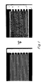
- FIGS. 1A and 1B there are shown photomicrographs illustrating the doubling of a grating of spatial period 2.54 ⁇ m of FIG. 1A by shadow printing it at a gap of about 8 ⁇ m, yielding a grating of 1.27 ⁇ m spatial period as shown in FIG. 1B.
- Both gratings have been RF sputter etched into chromium, using photoresist to mask against the etching in accordance with the common practice of microlithography.
- FIG. 2 there is shown a diagrammatic representation of the basic principles of spatial-period division embodied in the invention.
- a periodic array of slits a-d and a' -c' is illuminated with radiant energy of wavelength A from a distant point source. Radiation from slits a and a' will be in phase, and produce an intensity maximum at point a for all distances S. However, at a certain distance S 2 , the difference in length between paths a', ⁇ and a ⁇ will be one wavelength, and the path length from the remaining slits to ⁇ will differ from a ⁇ by integral multiples of the wavelength ⁇ . The result is an intensity maximum at ⁇ , and by symmetry, also at ⁇ '.
- the intensity patterns of the spatial-frequency multiples are a function of the widths of the slits in the parent mask. For monochromatic collimated radiation the three db width of the intensity peaks is approximately equal to the width of the slits.
- the intensity patterns of the spatial-frequency-multiples will be approximately sinusoidal superimposed on a low level background, as illustrated in FIG. 9. Such patterns are adequate for exposure of high contrast resists, such as PMMA, over depth-of-field, ⁇ S n , given
- An oblique-shadowing technique such as described in our copending application, Attorney's Reference GJE 5180/066, entitled "A Method of Producing X-Ray Masks" incorporated herein by reference, was used to produce a first mask having absorber stripes effectively 40nm wide.
- This first mask was then "reversed in polarity" upon a second mask, using a lift-off process, to yield a mask with 40 nm wide opening in gold 40 nm thick.
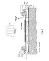
- the second mask was then used to produce a third mask using the process, of Figure 3A-3G which shows, in section, a fragmentary portion of the mask as it is processed.
- the mask includes PMMA high-resolution X-ray-sensitive resist 11 on a first polyimide layer 12 with a gold plating base 13 sandwiched between layer 12 and a second polyimide layer 14 that is on a glass substrate 15.
- the PMMA is then X-ray exposed and developed to form slits 16 exposing the surface of the first polyimide layer 12 as shown in FIG. 3B.
- Chrome is then evaporated on the surface to form the chrome layer 17 as shown in FIG. 3C.
- the PMMA is then dissolved so that only the chrome strips 17 that were in the gaps 16 remain on the first polyimide surface 12 as shown in FIG. 3D.
- the first polyimide layer 12 is then oxygen ion beam-etched away except beneath the chrome strips 17 to expose the surface of the gold plating base 13 as shown in 3E.
- the exposed gold plating base 13 is electroplated with a gold layer 21 as shown in FIG. 3F.
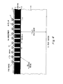
- glass layer 15 is removed to complete the mask as shown in FIG. 3G with the bars formed by polyimide layer 12 and chrome 17 defining the slit widths and the separation between centers of these slits being the parent mask spatial period. Referring to FIG. 4, there is shown a cross section of a completed parent mask drawn substantially to scale with specific dimensions as set forth corresponding essentially to the structure of FIG. 3G but covered with an aluminum film 22.
- the gap S between the grating of the parent mask at plating base 13 and the resist film should be approximately 4.3 ⁇ m.
- FIG. 5 there is shown in cross section an assembly including means for establishing and controlling this gap for exposing a PMMA resist 31 over a silicon oxide layer 32 on a silicon substrate 33 through parent mask 30 supported by spacer 34.
- Spacer 34 comprises solid members typically polyimide 35 between aluminum films 37. These solid portions attenuate the carbon K X-rays by about 9 db so that the image on photoresist 31 beneath them is underexposed.
- Penumbra due to the finite size of the source of carbon K X-rays 38, determine how close the assembly of FIG. 5 could be brought to the X-ray source, and thus determine exposure time.
- D the source-to-mask distance
- S the mask-to-substrate gap
- d the source diameter.
- S 4.3 pm
- A should be less than 196.8 nm/4.
- the source diameter was 1 mm, and thus D should be greater than 87 mm and was 115 mm, corresponding to an exposure time of 21 hours for the carbon K source operated at 4.8 kV and 70 ma.
- a synchrotron source of X-rays is preferred to allow shorter exposure times.
- Table 1 lists exposure times for a variety of spatial-frequency multiples and two parent mask periods for a synchrotron source. Alternatively, exposure times may be reduced by using a source of smaller diameter or linear geometry, or hot plasma sources.
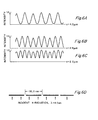
- FIGS. 6A-6C there is shown a graphical representation of the calculated intensity for second, third and fourth spatial-frequency multiples, respectively, of the 196.8 nm. grating shown in FIG. 6D.
- the plots were calculated numerically, taking into account the angular divergence of the X-rays from the source.
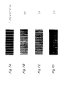
- FIGS. 7A-7D there are shown photomicrographs of the parent mask, 7A, and of spatial frequency quadrupling, tripling and doubling, FIGS. 7B, C and D, respectively, produced in photographic film. Exposure was done through the parent mask with an incandescent lamp through an orange filter.
- FIG. 8 there is shown an electron micrograph of the pattern developed in the PMMA layer 31 of FIG. 5.
- a 98.4 nm spatial-period grating was produced by spatial-period division, that is the second spatial-frequency multiple of the 196.8 nm X-ray parent mask 30.
- the parent mask 30 producing the result in FIG. 8 was not the ideal structure of FIG. 4; gold having over-plated the slots in the polyimide layer 12 and bridged across.
- the invention can be extended down to the limit of microlithography, believed to be about 10 nm spatial period.
- the absorbing regions of the parent mask should have a high attenuation, preferably greater than 20 db. Otherwise, the radiation transmitted through the absorber can interfere with the diffracted radiation to produce undesirable spatial-harmonic components. Alternatively, if 50% of the incident radiation is phase shifted by ⁇ in passing through the mask pattern, the zero-order diffracted beam can be canceled as explained in (15). If p ⁇ 2X,only the first-order diffracted beams will be present, and their interference will produce only the second spatial-frequency multiple. At optical and UV wavelengths, it is easy to achieve both zero-order cancellation and p ⁇ 2 ⁇ .
- the parent mask introduces a phase shift of ⁇ , thereby cancelling the zero-order beam and p ⁇ 2 ⁇ , doubling of any spatial frequency occurs at all distances.
- This feature enables doubling of quasi-periodic structures such as variable period gratings, grids and Fresnel zone plates that may be useful in making structures for X-ray imaging and spectroscopy.
- particles such as electrons, ions and neutrons can also be used for spatial-period-division, by virtue of their wave nature.
Landscapes
- Physics & Mathematics (AREA)
- General Physics & Mathematics (AREA)
- Engineering & Computer Science (AREA)
- Manufacturing & Machinery (AREA)
- Optics & Photonics (AREA)
- Health & Medical Sciences (AREA)
- Toxicology (AREA)
- Exposure And Positioning Against Photoresist Photosensitive Materials (AREA)
Applications Claiming Priority (4)
| Application Number | Priority Date | Filing Date | Title |
|---|---|---|---|
| US4331079A | 1979-05-29 | 1979-05-29 | |
| US43310 | 1979-05-29 | ||
| US06/140,150 US4360586A (en) | 1979-05-29 | 1980-04-14 | Spatial period division exposing |
| US140150 | 1980-04-14 |
Publications (3)
| Publication Number | Publication Date |
|---|---|
| EP0020132A2 true EP0020132A2 (de) | 1980-12-10 |
| EP0020132A3 EP0020132A3 (en) | 1981-08-19 |
| EP0020132B1 EP0020132B1 (de) | 1984-09-26 |
Family
ID=26720269
Family Applications (1)
| Application Number | Title | Priority Date | Filing Date |
|---|---|---|---|
| EP80301759A Expired EP0020132B1 (de) | 1979-05-29 | 1980-05-28 | Verfahren und Vorrichtung zum Herstellen eines Beugungsmittels |
Country Status (3)
| Country | Link |
|---|---|
| US (1) | US4360586A (de) |
| EP (1) | EP0020132B1 (de) |
| DE (1) | DE3069266D1 (de) |
Cited By (9)
| Publication number | Priority date | Publication date | Assignee | Title |
|---|---|---|---|---|
| EP0065115A1 (de) * | 1981-05-20 | 1982-11-24 | International Business Machines Corporation | Justiereinrichtung für Röntgen- oder optische Lithografie |
| EP0140175A3 (en) * | 1983-11-03 | 1987-08-12 | International Business Machines Corporation | Fresnel phase reversal plate lens and method for manufacturing such lenses |
| EP0242574A3 (en) * | 1986-04-04 | 1989-10-04 | Kernforschungszentrum Karlsruhe Gmbh | Procedure for the manufacture of an optical component having one or more echelette-gratings and device thereby obtained |
| EP0742455A1 (de) * | 1995-04-13 | 1996-11-13 | Dr. Johannes Heidenhain GmbH | Phasengitter und Verfahren zur Herstellung eines Phasengitters |
| EP0997781A1 (de) * | 1998-10-27 | 2000-05-03 | Canon Kabushiki Kaisha | Belichtungsverfahren |
| EP0997779A1 (de) * | 1998-10-29 | 2000-05-03 | Canon Kabushiki Kaisha | Belichtungsverfahren und Röntgenstrahlmaske dafür |
| DE10025694A1 (de) * | 2000-05-24 | 2002-03-07 | Zeiss Carl | Beugungsgitter sowie Verwendungen eines Beugungsgitters |
| CN103080843A (zh) * | 2010-07-07 | 2013-05-01 | 尤利塔股份公司 | 用于印刷具有大焦深的周期图案的方法和设备 |
| CN105259739A (zh) * | 2015-11-12 | 2016-01-20 | 中国科学院光电技术研究所 | 基于紫外宽光谱自成像制备二维周期阵列的光刻方法及装置 |
Families Citing this family (50)
| Publication number | Priority date | Publication date | Assignee | Title |
|---|---|---|---|---|
| CA1270934C (en) * | 1985-03-20 | 1990-06-26 | SPATIAL PHASE MODULATED MASKS AND METHODS FOR MAKING THESE MASKS AND PHASE DIFFRACTION GRATINGS | |
| US4846552A (en) * | 1986-04-16 | 1989-07-11 | The United States Of America As Represented By The Secretary Of The Air Force | Method of fabricating high efficiency binary planar optical elements |
| US5340637A (en) * | 1986-09-16 | 1994-08-23 | Hitachi, Ltd. | Optical device diffraction gratings and a photomask for use in the same |
| US4890309A (en) * | 1987-02-25 | 1989-12-26 | Massachusetts Institute Of Technology | Lithography mask with a π-phase shifting attenuator |
| DE3883638T2 (de) * | 1987-06-27 | 1994-04-21 | Shimadzu Corp | Flexibles Replika-Gitter und optischer Multiplexer/Demultiplexer mit Anwendung eines solchen Gitters. |
| US4947413A (en) * | 1988-07-26 | 1990-08-07 | At&T Bell Laboratories | Resolution doubling lithography technique |
| JP2710967B2 (ja) | 1988-11-22 | 1998-02-10 | 株式会社日立製作所 | 集積回路装置の製造方法 |
| JP2786693B2 (ja) * | 1989-10-02 | 1998-08-13 | 株式会社日立製作所 | マスクの製造方法 |
| US5342713A (en) * | 1990-06-21 | 1994-08-30 | Oki Electric Industry Co., Ltd. | Phase shifting mask |
| KR0172816B1 (ko) * | 1991-01-14 | 1999-03-30 | 문정환 | 마스크 제조방법 |
| US5217830A (en) * | 1991-03-26 | 1993-06-08 | Micron Technology, Inc. | Method of fabricating phase shifting reticles using ion implantation |
| US5194344A (en) * | 1991-03-26 | 1993-03-16 | Micron Technology, Inc. | Method of fabricating phase shift reticles including chemically mechanically planarizing |
| US5194346A (en) * | 1991-04-15 | 1993-03-16 | Micron Technology, Inc. | Method of fabricating phase shifting reticles with an accurate phase shift layer |
| US5194345A (en) * | 1991-05-14 | 1993-03-16 | Micron Technology, Inc. | Method of fabricating phase shift reticles |
| US5240796A (en) * | 1991-07-09 | 1993-08-31 | Micron Technology, Inc. | Method of fabricating a chromeless phase shift reticle |
| US5187726A (en) * | 1991-09-30 | 1993-02-16 | Wisconsin Alumni Research Foundation | High resolution X-ray lithography using phase shift masks |
| US5455850A (en) * | 1991-11-01 | 1995-10-03 | The Regents Of The Univerity Of Calif. | X-ray lithography using holographic images |
| US5272024A (en) * | 1992-04-08 | 1993-12-21 | International Business Machines Corporation | Mask-structure and process to repair missing or unwanted phase-shifting elements |
| US5288569A (en) * | 1992-04-23 | 1994-02-22 | International Business Machines Corporation | Feature biassing and absorptive phase-shifting techniques to improve optical projection imaging |
| US5260558A (en) * | 1992-05-20 | 1993-11-09 | Massachusetts Institute Of Technology | Measurements using balanced illumination optical microscopy |
| US5700602A (en) * | 1992-08-21 | 1997-12-23 | Intel Corporation | Method and apparatus for precision determination of phase-shift in a phase-shifted reticle |
| US5348826A (en) * | 1992-08-21 | 1994-09-20 | Intel Corporation | Reticle with structurally identical inverted phase-shifted features |
| JP2864915B2 (ja) * | 1992-12-07 | 1999-03-08 | 株式会社日立製作所 | 半導体装置の製造方法 |
| US5411824A (en) * | 1993-01-21 | 1995-05-02 | Sematech, Inc. | Phase shifting mask structure with absorbing/attenuating sidewalls for improved imaging |
| US5418095A (en) * | 1993-01-21 | 1995-05-23 | Sematech, Inc. | Method of fabricating phase shifters with absorbing/attenuating sidewalls using an additive process |
| WO1994017449A1 (en) * | 1993-01-21 | 1994-08-04 | Sematech, Inc. | Phase shifting mask structure with multilayer optical coating for improved transmission |
| US5362584A (en) * | 1993-04-02 | 1994-11-08 | International Business Machines Corporation | Phase-shifting transparent lithographic mask for writing contiguous structures from noncontiguous mask areas |
| US5446521A (en) * | 1993-06-30 | 1995-08-29 | Intel Corporation | Phase-shifted opaquing ring |
| US5420719A (en) * | 1993-09-15 | 1995-05-30 | Lumonics Inc. | Laser beam frequency doubling system |
| KR0151427B1 (ko) * | 1994-03-04 | 1999-02-18 | 문정환 | 위상 반전마스크 및 그의 제조방법 |
| KR960002536A (de) * | 1994-06-29 | 1996-01-26 | ||
| JP3290862B2 (ja) * | 1994-09-29 | 2002-06-10 | 株式会社東芝 | フォトマスクとこのフォトマスクを用いた露光方法及びこのフォトマスクの製造方法 |
| US5595843A (en) * | 1995-03-30 | 1997-01-21 | Intel Corporation | Layout methodology, mask set, and patterning method for phase-shifting lithography |
| US6671235B1 (en) | 2000-03-27 | 2003-12-30 | Ultratech Stepper, Inc. | Method of and apparatus for defining disk tracks in magnetic recording media |
| EP1447714A3 (de) * | 2003-02-14 | 2005-02-16 | Paul Scherrer Institut | Verfahren zur Erzeugung einer kreisförmigen periodischen Struktur auf einem Basisträgermaterial |
| US7858268B2 (en) * | 2003-02-14 | 2010-12-28 | Eulitha Ag | Method for generating a circular periodic structure on a basic support material |
| CZ2004234A3 (cs) * | 2004-02-12 | 2005-03-16 | Optaglio S. R. O. | Kovová identifikační šupina a způsob její výroby |
| DE602005026968D1 (de) * | 2004-10-22 | 2011-04-28 | Eulitha Ag | System und verfahren zum erzeugen eines periodischen und/oder fastperiodischen musters auf einer probe |
| US8368871B2 (en) * | 2010-02-16 | 2013-02-05 | Eulitha Ag | Lithographic fabrication of general periodic structures |
| US9036133B2 (en) | 2010-02-16 | 2015-05-19 | Eulitha Ag | Lithographic fabrication of general periodic structures by exposing a photosensitive layer to a range of lateral intensity distributions |
| US9007566B2 (en) | 2010-07-07 | 2015-04-14 | Eulitha Ag | Apparatus and method for printing a periodic pattern with a large depth of focus |
| US8525973B2 (en) | 2010-10-13 | 2013-09-03 | Eulitha A.G. | Method and apparatus for printing periodic patterns |
| US8904316B2 (en) | 2010-11-16 | 2014-12-02 | Eulitha A.G. | Method and apparatus for printing high-resolution two-dimensional periodic patterns |
| WO2012095795A2 (en) | 2011-01-12 | 2012-07-19 | Eulitha A.G. | Method and system for printing high-resolution periodic patterns |
| EP2715453A1 (de) | 2011-06-01 | 2014-04-09 | Eulitha A.G. | Drucken von periodischen mustern anhand mehrerer laser |
| US9859028B2 (en) * | 2012-03-08 | 2018-01-02 | Max-Planck-Gesellschaft Zur Foerderung Der Wissenschaften E.V. | Method of producing a Fresnel Zone Plate for applications in high energy radiation |
| EP2976678B1 (de) | 2013-03-18 | 2017-06-14 | Eulitha A.G. | Verfahren und systeme zum drucken periodischer muster |
| CN103245991B (zh) * | 2013-04-02 | 2015-08-12 | 厦门大学 | 一种倍频光栅空间频率的方法 |
| WO2017103817A1 (en) | 2015-12-14 | 2017-06-22 | Eulitha A.G. | Methods and systems for printing arrays of features |
| US11042098B2 (en) * | 2019-02-15 | 2021-06-22 | Applied Materials, Inc. | Large area high resolution feature reduction lithography technique |
Family Cites Families (6)
| Publication number | Priority date | Publication date | Assignee | Title |
|---|---|---|---|---|
| DE1285763B (de) * | 1967-11-08 | 1968-12-19 | Wenczler & Heidenhain | Verfahren zur Herstellung optischer Beugungsgitter |
| US3728117A (en) * | 1968-01-20 | 1973-04-17 | Heidenhain J Fa | Optical diffraction grid |
| US3615449A (en) * | 1969-09-25 | 1971-10-26 | Rca Corp | Method of generating high area-density periodic arrays by diffraction imaging |
| US3640197A (en) * | 1970-01-22 | 1972-02-08 | Motorola Inc | Production of fine single lines and of discrete closely spaced fine lines |
| DE2116713B2 (de) * | 1971-04-06 | 1974-03-28 | Ibm Deutschland Gmbh, 7000 Stuttgart | Belichtungsverfahren zum Abbilden sehr fein strukturierter Lichtmuster auf Photolackschichten und dazu geeignete Belichtungsvorrichtung |
| US3761264A (en) * | 1971-10-12 | 1973-09-25 | Rca Corp | Method of defining a detailed pattern on a surface of a body |
-
1980
- 1980-04-14 US US06/140,150 patent/US4360586A/en not_active Expired - Lifetime
- 1980-05-28 DE DE8080301759T patent/DE3069266D1/de not_active Expired
- 1980-05-28 EP EP80301759A patent/EP0020132B1/de not_active Expired
Cited By (18)
| Publication number | Priority date | Publication date | Assignee | Title |
|---|---|---|---|---|
| EP0065115A1 (de) * | 1981-05-20 | 1982-11-24 | International Business Machines Corporation | Justiereinrichtung für Röntgen- oder optische Lithografie |
| EP0140175A3 (en) * | 1983-11-03 | 1987-08-12 | International Business Machines Corporation | Fresnel phase reversal plate lens and method for manufacturing such lenses |
| EP0242574A3 (en) * | 1986-04-04 | 1989-10-04 | Kernforschungszentrum Karlsruhe Gmbh | Procedure for the manufacture of an optical component having one or more echelette-gratings and device thereby obtained |
| EP0742455A1 (de) * | 1995-04-13 | 1996-11-13 | Dr. Johannes Heidenhain GmbH | Phasengitter und Verfahren zur Herstellung eines Phasengitters |
| US5786931A (en) * | 1995-04-13 | 1998-07-28 | Johannes Heidenhain Gmbh | Phase grating and method of producing phase grating |
| US6327332B1 (en) | 1998-10-27 | 2001-12-04 | Canon Kabushiki Kaisha | Exposure method |
| EP0997781A1 (de) * | 1998-10-27 | 2000-05-03 | Canon Kabushiki Kaisha | Belichtungsverfahren |
| US6647087B2 (en) | 1998-10-27 | 2003-11-11 | Canon Kabushiki Kaisha | Exposure method |
| EP0997779A1 (de) * | 1998-10-29 | 2000-05-03 | Canon Kabushiki Kaisha | Belichtungsverfahren und Röntgenstrahlmaske dafür |
| US6272202B1 (en) | 1998-10-29 | 2001-08-07 | Canon Kabushiki Kaisha | Exposure method and X-ray mask structure for use with the same |
| KR100412017B1 (ko) * | 1998-10-29 | 2003-12-24 | 캐논 가부시끼가이샤 | 노광방법 및 이 방법용 x선마스크구조체 |
| DE10025694A1 (de) * | 2000-05-24 | 2002-03-07 | Zeiss Carl | Beugungsgitter sowie Verwendungen eines Beugungsgitters |
| DE10025694C2 (de) * | 2000-05-24 | 2003-06-05 | Zeiss Carl | Verwendung eines Beugungsgitters |
| US6600602B2 (en) | 2000-05-24 | 2003-07-29 | Carl-Zeiss Stiftung | Diffraction grating and uses of a diffraction grating |
| CN103080843A (zh) * | 2010-07-07 | 2013-05-01 | 尤利塔股份公司 | 用于印刷具有大焦深的周期图案的方法和设备 |
| CN103080843B (zh) * | 2010-07-07 | 2015-11-25 | 尤利塔股份公司 | 用于印刷具有大焦深的周期图案的方法和设备 |
| CN105259739A (zh) * | 2015-11-12 | 2016-01-20 | 中国科学院光电技术研究所 | 基于紫外宽光谱自成像制备二维周期阵列的光刻方法及装置 |
| CN105259739B (zh) * | 2015-11-12 | 2017-06-30 | 中国科学院光电技术研究所 | 基于紫外宽光谱自成像制备二维周期阵列的光刻方法及装置 |
Also Published As
| Publication number | Publication date |
|---|---|
| EP0020132A3 (en) | 1981-08-19 |
| US4360586A (en) | 1982-11-23 |
| EP0020132B1 (de) | 1984-09-26 |
| DE3069266D1 (en) | 1984-10-31 |
Similar Documents
| Publication | Publication Date | Title |
|---|---|---|
| EP0020132A2 (de) | Verfahren und Vorrichtung zum Herstellen eines Beugungsmittels | |
| US4890309A (en) | Lithography mask with a π-phase shifting attenuator | |
| JP3078163B2 (ja) | リソグラフィ用反射型マスクおよび縮小投影露光装置 | |
| Yang | Fresnel and refractive lenses for X-rays | |
| KR100213605B1 (ko) | 패턴형성방법 및 투영노출장치 | |
| KR910007220B1 (ko) | 리소그래피 시스템 및 그의 해상도 증진 방법 | |
| EP1810085B1 (de) | System und verfahren zum erzeugen eines periodischen und/oder fastperiodischen musters auf einer probe | |
| US4028547A (en) | X-ray photolithography | |
| JPH08139013A (ja) | 電子線描画装置及び電子線描画方法 | |
| US5372916A (en) | X-ray exposure method with an X-ray mask comprising phase shifter sidewalls | |
| US5650632A (en) | Focal plane phase-shifting lithography | |
| US6020950A (en) | Exposure method and projection exposure apparatus | |
| Lüttgenau et al. | Novel high-contrast phase-shifting masks for EUV interference lithography | |
| CA1153227A (en) | Method and apparatus for making grating | |
| JPH0588355A (ja) | 反射型マスク及びそれを用いた露光装置 | |
| David et al. | Wet-etched diffractive lenses for hard X-rays | |
| Guo et al. | Experimental and theoretical study of image bias in x‐ray lithography | |
| US5770335A (en) | Mask and exposure apparatus using the same | |
| Di Fabrizio et al. | Nano-optical elements fabricated by e-beam and x-ray lithography | |
| Vladimirsky et al. | Fabrication of free-standing X-ray transmission gratings and zone plates | |
| Babin et al. | Fabrication of diffraction X-ray elements | |
| JPH05346503A (ja) | ゾーンプレートの製造方法 | |
| JP3133618B2 (ja) | 縮小投影露光装置において用いられる空間フィルタ | |
| JP3267498B2 (ja) | マスク及びこれを用いたデバイス生産方法や露光装置 | |
| JPS63316434A (ja) | X線露光法 |
Legal Events
| Date | Code | Title | Description |
|---|---|---|---|
| PUAI | Public reference made under article 153(3) epc to a published international application that has entered the european phase |
Free format text: ORIGINAL CODE: 0009012 |
|
| AK | Designated contracting states |
Designated state(s): DE FR GB NL |
|
| PUAL | Search report despatched |
Free format text: ORIGINAL CODE: 0009013 |
|
| AK | Designated contracting states |
Designated state(s): DE FR GB NL |
|
| 17P | Request for examination filed |
Effective date: 19820219 |
|
| GRAA | (expected) grant |
Free format text: ORIGINAL CODE: 0009210 |
|
| AK | Designated contracting states |
Designated state(s): DE FR GB NL |
|
| REF | Corresponds to: |
Ref document number: 3069266 Country of ref document: DE Date of ref document: 19841031 |
|
| ET | Fr: translation filed | ||
| PLBE | No opposition filed within time limit |
Free format text: ORIGINAL CODE: 0009261 |
|
| STAA | Information on the status of an ep patent application or granted ep patent |
Free format text: STATUS: NO OPPOSITION FILED WITHIN TIME LIMIT |
|
| 26N | No opposition filed | ||
| PG25 | Lapsed in a contracting state [announced via postgrant information from national office to epo] |
Ref country code: NL Effective date: 19851201 |
|
| GBPC | Gb: european patent ceased through non-payment of renewal fee | ||
| NLV4 | Nl: lapsed or anulled due to non-payment of the annual fee | ||
| PG25 | Lapsed in a contracting state [announced via postgrant information from national office to epo] |
Ref country code: FR Free format text: LAPSE BECAUSE OF NON-PAYMENT OF DUE FEES Effective date: 19860131 |
|
| PG25 | Lapsed in a contracting state [announced via postgrant information from national office to epo] |
Ref country code: DE Effective date: 19860201 |
|
| REG | Reference to a national code |
Ref country code: FR Ref legal event code: ST |
|
| PG25 | Lapsed in a contracting state [announced via postgrant information from national office to epo] |
Ref country code: GB Effective date: 19881118 |
|
| PGFP | Annual fee paid to national office [announced via postgrant information from national office to epo] |
Ref country code: FR Payment date: 19910430 Year of fee payment: 12 |