EP0016577A1 - Semiconductor integrated circuit device with a double interconnection layer - Google Patents
Semiconductor integrated circuit device with a double interconnection layer Download PDFInfo
- Publication number
- EP0016577A1 EP0016577A1 EP19800300661 EP80300661A EP0016577A1 EP 0016577 A1 EP0016577 A1 EP 0016577A1 EP 19800300661 EP19800300661 EP 19800300661 EP 80300661 A EP80300661 A EP 80300661A EP 0016577 A1 EP0016577 A1 EP 0016577A1
- Authority
- EP
- European Patent Office
- Prior art keywords
- layer
- wiring layer
- integrated circuit
- circuit device
- semiconductor integrated
- Prior art date
- Legal status (The legal status is an assumption and is not a legal conclusion. Google has not performed a legal analysis and makes no representation as to the accuracy of the status listed.)
- Granted
Links
- 239000004065 semiconductor Substances 0.000 title claims abstract description 37
- 238000009413 insulation Methods 0.000 claims abstract description 19
- 239000000758 substrate Substances 0.000 claims abstract description 17
- 239000000463 material Substances 0.000 claims abstract description 7
- 230000005669 field effect Effects 0.000 claims description 7
- 229910021420 polycrystalline silicon Inorganic materials 0.000 description 47
- 238000000034 method Methods 0.000 description 21
- VYPSYNLAJGMNEJ-UHFFFAOYSA-N Silicium dioxide Chemical compound O=[Si]=O VYPSYNLAJGMNEJ-UHFFFAOYSA-N 0.000 description 20
- 229910052814 silicon oxide Inorganic materials 0.000 description 19
- 239000004411 aluminium Substances 0.000 description 10
- 229910052782 aluminium Inorganic materials 0.000 description 10
- XAGFODPZIPBFFR-UHFFFAOYSA-N aluminium Chemical compound [Al] XAGFODPZIPBFFR-UHFFFAOYSA-N 0.000 description 10
- 239000012535 impurity Substances 0.000 description 7
- 230000003647 oxidation Effects 0.000 description 7
- 238000007254 oxidation reaction Methods 0.000 description 7
- 229910052751 metal Inorganic materials 0.000 description 4
- 239000002184 metal Substances 0.000 description 4
- OAICVXFJPJFONN-UHFFFAOYSA-N Phosphorus Chemical compound [P] OAICVXFJPJFONN-UHFFFAOYSA-N 0.000 description 3
- 238000005229 chemical vapour deposition Methods 0.000 description 3
- 229910052698 phosphorus Inorganic materials 0.000 description 3
- 239000011574 phosphorus Substances 0.000 description 3
- ZOXJGFHDIHLPTG-UHFFFAOYSA-N Boron Chemical compound [B] ZOXJGFHDIHLPTG-UHFFFAOYSA-N 0.000 description 2
- 229910052796 boron Inorganic materials 0.000 description 2
- 238000010276 construction Methods 0.000 description 2
- 238000009792 diffusion process Methods 0.000 description 2
- 230000005684 electric field Effects 0.000 description 2
- 238000005530 etching Methods 0.000 description 2
- 239000012212 insulator Substances 0.000 description 2
- 238000004519 manufacturing process Methods 0.000 description 2
- XUIMIQQOPSSXEZ-UHFFFAOYSA-N Silicon Chemical compound [Si] XUIMIQQOPSSXEZ-UHFFFAOYSA-N 0.000 description 1
- 229910021419 crystalline silicon Inorganic materials 0.000 description 1
- 230000003247 decreasing effect Effects 0.000 description 1
- 239000002019 doping agent Substances 0.000 description 1
- 229910044991 metal oxide Inorganic materials 0.000 description 1
- 150000004706 metal oxides Chemical class 0.000 description 1
- 238000012986 modification Methods 0.000 description 1
- 230000004048 modification Effects 0.000 description 1
- 229910052710 silicon Inorganic materials 0.000 description 1
- 239000010703 silicon Substances 0.000 description 1
- 239000002210 silicon-based material Substances 0.000 description 1
Images

Classifications
-
- H—ELECTRICITY
- H01—ELECTRIC ELEMENTS
- H01L—SEMICONDUCTOR DEVICES NOT COVERED BY CLASS H10
- H01L23/00—Details of semiconductor or other solid state devices
- H01L23/52—Arrangements for conducting electric current within the device in operation from one component to another, i.e. interconnections, e.g. wires, lead frames
- H01L23/522—Arrangements for conducting electric current within the device in operation from one component to another, i.e. interconnections, e.g. wires, lead frames including external interconnections consisting of a multilayer structure of conductive and insulating layers inseparably formed on the semiconductor body
- H01L23/528—Geometry or layout of the interconnection structure
- H01L23/5283—Cross-sectional geometry
-
- H—ELECTRICITY
- H01—ELECTRIC ELEMENTS
- H01L—SEMICONDUCTOR DEVICES NOT COVERED BY CLASS H10
- H01L29/00—Semiconductor devices adapted for rectifying, amplifying, oscillating or switching, or capacitors or resistors with at least one potential-jump barrier or surface barrier, e.g. PN junction depletion layer or carrier concentration layer; Details of semiconductor bodies or of electrodes thereof ; Multistep manufacturing processes therefor
- H01L29/40—Electrodes ; Multistep manufacturing processes therefor
- H01L29/43—Electrodes ; Multistep manufacturing processes therefor characterised by the materials of which they are formed
- H01L29/49—Metal-insulator-semiconductor electrodes, e.g. gates of MOSFET
- H01L29/51—Insulating materials associated therewith
- H01L29/511—Insulating materials associated therewith with a compositional variation, e.g. multilayer structures
-
- H—ELECTRICITY
- H01—ELECTRIC ELEMENTS
- H01L—SEMICONDUCTOR DEVICES NOT COVERED BY CLASS H10
- H01L29/00—Semiconductor devices adapted for rectifying, amplifying, oscillating or switching, or capacitors or resistors with at least one potential-jump barrier or surface barrier, e.g. PN junction depletion layer or carrier concentration layer; Details of semiconductor bodies or of electrodes thereof ; Multistep manufacturing processes therefor
- H01L29/40—Electrodes ; Multistep manufacturing processes therefor
- H01L29/43—Electrodes ; Multistep manufacturing processes therefor characterised by the materials of which they are formed
- H01L29/49—Metal-insulator-semiconductor electrodes, e.g. gates of MOSFET
- H01L29/51—Insulating materials associated therewith
-
- H—ELECTRICITY
- H01—ELECTRIC ELEMENTS
- H01L—SEMICONDUCTOR DEVICES NOT COVERED BY CLASS H10
- H01L2924/00—Indexing scheme for arrangements or methods for connecting or disconnecting semiconductor or solid-state bodies as covered by H01L24/00
- H01L2924/0001—Technical content checked by a classifier
- H01L2924/0002—Not covered by any one of groups H01L24/00, H01L24/00 and H01L2224/00
Definitions
- This invention relates to a semiconductor integrated circuit device with a double interconnection layer consisting of semiconductive material.
- Interconnections have been formed in prior semiconductor integrated circuit device by means of metal layers diffusion regions formed in the semiconductive substrate, polycrystalline silicon layers and so on.
- the resistance value of the interconnection means or "wiring layer” is preferred to be smaller, so metal layers for example aluminium layers are preferred.
- the interconnections cannot be formed by a single metal layer, because it may be necessary for several wiring layers to cross at one point. In such a case one layer may comprise for'example a polycrystalline silicon layer as a wiring means at the crossing point, whilst a second wiring layer made of metal is formed over the first wiring layer with an insulating layer interleaved between the two layers.
- the polycrystalline silicon layer may be used as the electrode of a metal oxide semiconductor field effect transistor (herein after called MOS FET).
- MOS FET metal oxide semiconductor field effect transistor
- the sheet resistance can be lowered by increasing the level of doping, but as the doping level increases it becomes more difficult to control the etching process.
- the quantity of impurity which can be introduced into the polycrystalline silicon as dopant is restricted by the precision of the etching process, so the most commonly used form of doped polycrystalline silicon has a sheet resistance of about 44 ⁇ / ⁇ to 50 ⁇ / ⁇ , which is much higher than that of metal-layers for example aluminium layers, so the operating speed and flexibility of . design of the circuit will be limited.
- Another method of decreasing the resistance of the polycrystalline silicon layer is to increase its thickness and width.
- This can give rise to the disadvantage that the aluminium layer thereover may be pierced by--the sharp edge of the thick polycrystalline silicon layer, and the increase of width will result in an increase the increase of the total area of the device.
- the present invention seeks to provide a semiconductor integrated circuit device which can be constructed in high density form and which can operate at high speed.
- the invention also seeks to provide a semiconductor integrated circuit device including wiring layers whose resistance is kept low.
- a semiconductor integrated circuit device including a main wiring layer and a secondary wiring layer connected in parallel therewith.
- Another aspect of this invention is to provide a semiconductor integrated circuit device which includes two semiconductor wiring layers, one layer operating as a gate electrode of a MOS FET and the other layer being connected in parallel to said one layer so as to decrease the total resistance.
- a further aspect of the present invention is the provision of a semiconductor integrated circuit device comprising a semiconductor substrate on which an insulation layer is formed, a'first wiring layer made of semiconductive material and positioned on said insulation layer and a second wiring layer made of semiconductive material formed over said first layer and connected in parallel to said first wiring layer.
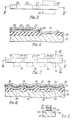
- FIG. 1 and Figure 2 on the upper surface of the n-type semiconductor substrate (1) is provided an insulation layer (2).
- the substrate (1) is of silicon (Si) and the layer (2) is made of silicon oxide (Si0 2 ).
- the insulation layer (2) has a thickness of about seven or eight thousand angstroms and is formed by chemical vapour deposition technique, and the polycrystalline silicon layer (3) covers selected portions thereof with a thickness of about three thousand angstroms.
- the polycrystalline silicon layer (3) is formed to cover the whole surface of the insulation layer (2), and subsequently it is partially etched away by a photo-engraving process.
- the surface of the polycrystalline silicon layer (3) is then oxidized using a thermal oxidation process to form a silicon oxide layer (4).
- the silicon oxide layer (4) has a thickness of about one thousand angstroms and has two contact holes (5) and (6).
- the holes (5) and (6) are formed by the photo-engraving process.
- a second polycrystalline silicon layer (7) is formed over the silicon oxide layer (4) with a thickness of about three of four thousand angstroms and makes contact with the first polycrystalline silicon layer (3) through the contact holes (5) and (6).
- the second polycrystalline silicon layer (7) is formed in substantially the same pattern as the first polycrystalline silicon layer (3) and operates as the main wiring layer.
- An insulation layer (8) is formed to cover them.
- the insulation layer (8) is made of silicon oxide and has a thickness of 1.3 micron. In this embodiment, the insulation layer (8) is formed by a chemical vapour deposition technique. After the covering process, two contact holes (9) and (10) are formed by photo engraving process.
- aluminium layers (11) and (12) applied over selected portions of the insulator layer (8) make contact with the second polycrystalline silicon layer (7).
- the aluminium layers (11) and (12) are connected through the polycrystalline silicon layers (3) and (7) to circuit elements formed on the substrate. Further, the aluminium layer (13) positioned on the insulator layer (8) crosses over the first and second polycrystalline silicon layer (3) and (7).
- the aluminium layers (11) and (12) and the polycrystalline silicon layers (3) and (7) operate together as wiring layers, their total resistance is low. The resistance of the aluminium is very low, but that of the polycrystalline silicon is higher than the aluminium.
- the polycrystalline silicon layers (3) and (7) are connected in parallel, so that their resistance is about one half of that of one polycrystalline silicon layer alone. Further, as the change in level at the edge of the two polycrystalline silicon layers is made less abrupt by the existence of the silicon oxide layer (4), the aluminium layers (11) and (12) will not be pierced by the edge. In order to further reduce the abruptness of the change of level, the layer 7 can be made slightly smaller so that its edge does not coincide with that of layer 4.
- Figures 3 and 4 show a second embodiment of this invention.
- a thick film silicon oxide layer (22) is formed by using a selective oxidation process.
- the first polycrystalline silicon layer (24) is formed on the selected portion of the silicon oxide layer (22).
- This layer (24) operates as the secondary wiring layer for a further polycrystalline silicon layer (25) formed thereover.
- the polycrystalline silicon layers (24) and (25) become conductive by doping with an impurity such as phosphorus, boron or the like.
- the polycrystalline silicon layer (24) is covered by a silicon oxide layer (26).
- the silicon oxide layer (26) has two contact holes (27) and (28) formed by a photo-engraving process and is formed by thermal oxidation of the surface of the polycrystalline silicon layer (24).
- a silicon oxide layer (23) forming the gate of a MOS FET and having a thickness of 1000i is formed at the same time, simplifying the manufacturing process.
- the second polycrystalline silicon layer (25) is then formed over the layer 26 and the exposed portions of layers 22 and 24.
- the polycrystalline silicon layer (25) thus operates as the gate electrode of the NOS FET and as a wiring layer, being connected in parallel with the first polycrystalline silicon layer (24) through the two contact holes (27) and (28) in order to decrease the resistance.
- the source region (29) and the drain region (30) of the MOS FET are formed in the substrate (21) by diffusing phosphorus as an N-type impurity using the gate silicon oxide layer (23) and the polycrystalline silicon layer (25) as a mask.
- FIGS 5 and 6 show the third embodiment of this invention.
- a plurality of MOS FETs are regularly arranged in the semiconductor substrate (31), and constitute a memory array. They are formed in the following way:
- a thick film silicon oxide layer (32) is formed on the selected portion of the p-type semiconductor substrate (31) by using a selective oxidation process. The thickness thereof is about seven or eight thousand angstroms.
- the gate silicon oxide layer (33) of the MOS FETs is formed using a thermal oxidation process. The thickness thereof is of about one thousand angstroms.
- the first polycrystalline silicon layer (34) operating both as a set of gate electrodes and as a wiring layer is formed on the selective portion of the silicon oxide layers (32) and (33).
- the first polycrystalline silicon layer (34) is then covered by silicon oxide layer (35).
- the silicon oxide layer (35) has contact holes (36) and is formed by thermal oxidation of the first polycrystalline silicon layer (34).
- the second crystalline silicon layer (37) is formed over the first polycrystalline silicon layer (34) in order to decrease the resistance of the wiring layer.
- the polycrystalline silicon layers (34) and (37) are made conductive by doping with a suitable impurity.
- the silicon oxide layer (35), the first polycrystalline silicon layer (34) and the gate silicon oxide layer (33) are etched using the second polycrystalline silicon layer (37) over the channel region of the MOS FETs as the mask so as to leave suitable portions positioned over the channel region of MOS FET to form masks for forming the source and drain regions.
- these layers (33), (34) and (35) will be formed with the same width as the second polycrystalline silicon layer (37).
- an n-type impurity is doped into the p-type substrate (31), and the source regions (38) and the drain regions (39) are formed therein.
- the length between source and drain regions (38) and (39) is equal to the width of the layers (34) and (37), (see Figure 7) so the electric field of the gate electrode (34) and (37) will be uniformly applied to the channel region.
- This method of construction avoids the possibility of the layer (37) being formed out of register with the layer (34), which could cause the length of the channel region to be non-uniform because of the gap between the two layers (34) and (37), so that the electric field of the gate electrode (34) and (37) would become non-uniform and the characteristics of the MOS FETs would become inferior.
- the channel length of MOS FET is made more uniform and the resistance of the wiring layer and the gate electrode is kept very low, so that the circuit will be able to operate at high speed and the whole device will be of compact construction and have superior electrical characteristics.
- connection between the first and second polycrystalline silicon layers can be accomplished by a greater number of contact holes or they may be laminated directly on one another. Then the connecting resistance may be made smaller, but the positioning of two layers and the whole process will become more critical, because the wiring pattern is generally very complicated.
- the contact holes for connecting the two layers can be formed at the same time that the direct contact holes, connecting the polycrystalline silicon layer and the diffusion layer in the substrate, are formed. Then the process will be simplified.
- the thermal oxidation process can be substituted by a chemical vapour deposition process, and a predoped polycrystalline silicon layer may be used instead of doping impurity into the polycrystalline layer during the manufacturing process.
Abstract
Description
- This invention relates to a semiconductor integrated circuit device with a double interconnection layer consisting of semiconductive material.
- Interconnections have been formed in prior semiconductor integrated circuit device by means of metal layers diffusion regions formed in the semiconductive substrate, polycrystalline silicon layers and so on. Generally, the resistance value of the interconnection means or "wiring layer" is preferred to be smaller, so metal layers for example aluminium layers are preferred. However, when the semiconductor integrated circuit is constructed in high density form, the interconnections cannot be formed by a single metal layer, because it may be necessary for several wiring layers to cross at one point. In such a case one layer may comprise for'example a polycrystalline silicon layer as a wiring means at the crossing point, whilst a second wiring layer made of metal is formed over the first wiring layer with an insulating layer interleaved between the two layers. Using this technique, it is easy to produce a semiconductive integrated circuit which includes crossing points of the wiring layers. Further, the polycrystalline silicon layer may be used as the electrode of a metal oxide semiconductor field effect transistor (herein after called MOS FET). When the gate electrode is constructed with polycrystalline silicon material, the MOS FET can be manufactured by a self-alignment process so that it will be formed compactly, and its operating characteristics will be improved.
- Thus recently polycrystalline silicon has frequently been used to form the wiring layers and electrodes. However, the sheet resistance of the polycrystalline silicon is very high and so doped polycrystalline silicon has come to be used instead, and has a sheet resistance of the order of several tens of Ω/□.
- The sheet resistance can be lowered by increasing the level of doping, but as the doping level increases it becomes more difficult to control the etching process. Thus the quantity of impurity which can be introduced into the polycrystalline silicon as dopant is restricted by the precision of the etching process, so the most commonly used form of doped polycrystalline silicon has a sheet resistance of about 44 Ω/□ to 50 Ω/□, which is much higher than that of metal-layers for example aluminium layers, so the operating speed and flexibility of . design of the circuit will be limited.
- Another method of decreasing the resistance of the polycrystalline silicon layer is to increase its thickness and width. However this can give rise to the disadvantage that the aluminium layer thereover may be pierced by--the sharp edge of the thick polycrystalline silicon layer, and the increase of width will result in an increase the increase of the total area of the device.
- Accordingly the present invention seeks to provide a semiconductor integrated circuit device which can be constructed in high density form and which can operate at high speed.
- The invention also seeks to provide a semiconductor integrated circuit device including wiring layers whose resistance is kept low.
- According to one aspect of the present invention there is provided a semiconductor integrated circuit device including a main wiring layer and a secondary wiring layer connected in parallel therewith.
- Another aspect of this invention is to provide a semiconductor integrated circuit device which includes two semiconductor wiring layers, one layer operating as a gate electrode of a MOS FET and the other layer being connected in parallel to said one layer so as to decrease the total resistance.
- A further aspect of the present invention is the provision of a semiconductor integrated circuit device comprising a semiconductor substrate on which an insulation layer is formed, a'first wiring layer made of semiconductive material and positioned on said insulation layer and a second wiring layer made of semiconductive material formed over said first layer and connected in parallel to said first wiring layer.
- Some embodiments of the invention will now be described by way of example with reference to the accompanying drawings, wherein:
- Figure 1 is a partial plan view of one embodiment of this invention.
- Figure 2 is a vertical cross-section on line II-II of Figure 1,
- Figure 3 is a partial plan view of another embodiment of this invention,
- Figure 4 is a vertical cross-section on line IV-IV of Figure 3
- Figure 5 is a partial plan view of another embodiment of this invention,
- Figure 6 is a vertical cross-section on line VI-VI of Figure 5; and
- Figure 7 is a vertical cross-section on line VII-VII of Figure 5.
- Referring now to the drawings, wherein like reference numerals designate identical of corresponding parts throughout the several views, and more particularly to Figures 1 and 2 thereof, one embodiment of the semiconductor integrated circuit device of this invention is illustrated. In Figure 1 and Figure 2, on the upper surface of the n-type semiconductor substrate (1) is provided an insulation layer (2). The substrate (1) is of silicon (Si) and the layer (2) is made of silicon oxide (Si02). The insulation layer (2) has a thickness of about seven or eight thousand angstroms and is formed by chemical vapour deposition technique, and the polycrystalline silicon layer (3) covers selected portions thereof with a thickness of about three thousand angstroms. Initially the polycrystalline silicon layer (3) is formed to cover the whole surface of the insulation layer (2), and subsequently it is partially etched away by a photo-engraving process. The addition of an impurity, such as phosphorus, boron,or the like, to the polycrystalline silicon layer (3), reduces its sheet resistance to about 40 Ω/□. . The surface of the polycrystalline silicon layer (3) is then oxidized using a thermal oxidation process to form a silicon oxide layer (4). The silicon oxide layer (4) has a thickness of about one thousand angstroms and has two contact holes (5) and (6). The holes (5) and (6) are formed by the photo-engraving process. Thereafter a second polycrystalline silicon layer (7) is formed over the silicon oxide layer (4) with a thickness of about three of four thousand angstroms and makes contact with the first polycrystalline silicon layer (3) through the contact holes (5) and (6). The second polycrystalline silicon layer (7) is formed in substantially the same pattern as the first polycrystalline silicon layer (3) and operates as the main wiring layer. An insulation layer (8) is formed to cover them. The insulation layer (8) is made of silicon oxide and has a thickness of 1.3 micron. In this embodiment, the insulation layer (8) is formed by a chemical vapour deposition technique. After the covering process, two contact holes (9) and (10) are formed by photo engraving process. Through the two contact holes (9) and (10), aluminium layers (11) and (12) applied over selected portions of the insulator layer (8) make contact with the second polycrystalline silicon layer (7). The aluminium layers (11) and (12) are connected through the polycrystalline silicon layers (3) and (7) to circuit elements formed on the substrate. Further, the aluminium layer (13) positioned on the insulator layer (8) crosses over the first and second polycrystalline silicon layer (3) and (7). As the aluminium layers (11) and (12) and the polycrystalline silicon layers (3) and (7) operate together as wiring layers, their total resistance is low. The resistance of the aluminium is very low, but that of the polycrystalline silicon is higher than the aluminium. Therefore the polycrystalline silicon layers (3) and (7) are connected in parallel, so that their resistance is about one half of that of one polycrystalline silicon layer alone. Further, as the change in level at the edge of the two polycrystalline silicon layers is made less abrupt by the existence of the silicon oxide layer (4), the aluminium layers (11) and (12) will not be pierced by the edge. In order to further reduce the abruptness of the change of level, the layer 7 can be made slightly smaller so that its edge does not coincide with that of layer 4.
- Figures 3 and 4 show a second embodiment of this invention. On a P type semiconductive substrate (21), a thick film silicon oxide layer (22) is formed by using a selective oxidation process. Next, the first polycrystalline silicon layer (24) is formed on the selected portion of the silicon oxide layer (22). This layer (24) operates as the secondary wiring layer for a further polycrystalline silicon layer (25) formed thereover.
- The polycrystalline silicon layers (24) and (25) become conductive by doping with an impurity such as phosphorus, boron or the like. The polycrystalline silicon layer (24) is covered by a silicon oxide layer (26). The silicon oxide layer (26) has two contact holes (27) and (28) formed by a photo-engraving process and is formed by thermal oxidation of the surface of the polycrystalline silicon layer (24). A silicon oxide layer (23) forming the gate of a MOS FET and having a thickness of 1000i is formed at the same time, simplifying the manufacturing process. The second polycrystalline silicon layer (25) is then formed over the
layer 26 and the exposed portions oflayers - Figures 5 and 6 show the third embodiment of this invention. In this embodiment, a plurality of MOS FETs are regularly arranged in the semiconductor substrate (31), and constitute a memory array. They are formed in the following way:
- A thick film silicon oxide layer (32) is formed on the selected portion of the p-type semiconductor substrate (31) by using a selective oxidation process. The thickness thereof is about seven or eight thousand angstroms. Next, the gate silicon oxide layer (33) of the MOS FETs is formed using a thermal oxidation process. The thickness thereof is of about one thousand angstroms. After that, the first polycrystalline silicon layer (34) operating both as a set of gate electrodes and as a wiring layer, is formed on the selective portion of the silicon oxide layers (32) and (33). The first polycrystalline silicon layer (34) is then covered by silicon oxide layer (35). The silicon oxide layer (35) has contact holes (36) and is formed by thermal oxidation of the first polycrystalline silicon layer (34). Then, the second crystalline silicon layer (37) is formed over the first polycrystalline silicon layer (34) in order to decrease the resistance of the wiring layer.
- These two layers (34) and (37) are connected through the holes (36). The polycrystalline silicon layers (34) and (37) are made conductive by doping with a suitable impurity.
- Next the silicon oxide layer (35), the first polycrystalline silicon layer (34) and the gate silicon oxide layer (33) are etched using the second polycrystalline silicon layer (37) over the channel region of the MOS FETs as the mask so as to leave suitable portions positioned over the channel region of MOS FET to form masks for forming the source and drain regions. In this way these layers (33), (34) and (35) will be formed with the same width as the second polycrystalline silicon layer (37).
- Thereafter, an n-type impurity is doped into the p-type substrate (31), and the source regions (38) and the drain regions (39) are formed therein. In this way, as the layers (33), (34), (35) and (37) with the same width are used as the mask, the length between source and drain regions (38) and (39) is equal to the width of the layers (34) and (37), (see Figure 7) so the electric field of the gate electrode (34) and (37) will be uniformly applied to the channel region. This method of construction, avoids the possibility of the layer (37) being formed out of register with the layer (34), which could cause the length of the channel region to be non-uniform because of the gap between the two layers (34) and (37), so that the electric field of the gate electrode (34) and (37) would become non-uniform and the characteristics of the MOS FETs would become inferior.
- According to this embodiment of the invention the channel length of MOS FET is made more uniform and the resistance of the wiring layer and the gate electrode is kept very low, so that the circuit will be able to operate at high speed and the whole device will be of compact construction and have superior electrical characteristics.
- Obviously, numerous modifications and variations of the present invention are possible in light of the above teachings. For example, the connection between the first and second polycrystalline silicon layers can be accomplished by a greater number of contact holes or they may be laminated directly on one another. Then the connecting resistance may be made smaller, but the positioning of two layers and the whole process will become more critical, because the wiring pattern is generally very complicated. Another possibility is that the contact holes for connecting the two layers can be formed at the same time that the direct contact holes, connecting the polycrystalline silicon layer and the diffusion layer in the substrate, are formed. Then the process will be simplified. Further, the thermal oxidation process can be substituted by a chemical vapour deposition process, and a predoped polycrystalline silicon layer may be used instead of doping impurity into the polycrystalline layer during the manufacturing process.
Claims (11)
Applications Claiming Priority (2)
| Application Number | Priority Date | Filing Date | Title |
|---|---|---|---|
| JP2736179A JPS55120150A (en) | 1979-03-09 | 1979-03-09 | Semiconductor device |
| JP27361/79 | 1979-03-09 |
Publications (2)
| Publication Number | Publication Date |
|---|---|
| EP0016577A1 true EP0016577A1 (en) | 1980-10-01 |
| EP0016577B1 EP0016577B1 (en) | 1983-04-13 |
Family
ID=12218902
Family Applications (1)
| Application Number | Title | Priority Date | Filing Date |
|---|---|---|---|
| EP19800300661 Expired EP0016577B1 (en) | 1979-03-09 | 1980-03-05 | Semiconductor integrated circuit device with a double interconnection layer |
Country Status (3)
| Country | Link |
|---|---|
| EP (1) | EP0016577B1 (en) |
| JP (1) | JPS55120150A (en) |
| DE (1) | DE3062675D1 (en) |
Cited By (7)
| Publication number | Priority date | Publication date | Assignee | Title |
|---|---|---|---|---|
| EP0080730A2 (en) * | 1981-11-30 | 1983-06-08 | Kabushiki Kaisha Toshiba | Semiconductor device with wiring layers and method of manufacturing the same |
| US4544941A (en) * | 1980-06-19 | 1985-10-01 | Tokyo Shibaura Denki Kabushiki Kaisha | Semiconductor device having multiple conductive layers and the method of manufacturing the semiconductor device |
| EP0170052A2 (en) * | 1984-07-02 | 1986-02-05 | Fujitsu Limited | Master slice type semiconductor circuit device |
| GB2181894A (en) * | 1985-10-16 | 1987-04-29 | Mitsubishi Electric Corp | Duplicate wiring in a semiconductor device |
| EP0250269A2 (en) * | 1986-06-19 | 1987-12-23 | Nec Corporation | Integrated circuit semiconductor device having improved wiring structure |
| GB2263018A (en) * | 1991-03-23 | 1993-07-07 | Sony Corp | Static random access memories |
| US5332688A (en) * | 1991-03-23 | 1994-07-26 | Sony Corporation | Method of manufacturing full CMOS type SRAM |
Families Citing this family (18)
| Publication number | Priority date | Publication date | Assignee | Title |
|---|---|---|---|---|
| JPS56161668A (en) * | 1980-05-16 | 1981-12-12 | Hitachi Ltd | Semiconductor device |
| JPS5756959A (en) * | 1980-09-22 | 1982-04-05 | Toshiba Corp | Semiconductor device and manufacture thereof |
| JPS5756958A (en) * | 1980-09-22 | 1982-04-05 | Toshiba Corp | Semiconductor device |
| JPS57194552A (en) * | 1981-05-25 | 1982-11-30 | Matsushita Electric Ind Co Ltd | Signal transmission line |
| JPS57211249A (en) * | 1981-06-22 | 1982-12-25 | Nec Corp | Integrated circuit device |
| JPS5834946A (en) * | 1981-08-27 | 1983-03-01 | Nec Corp | Semiconductor integrated circuit device |
| JPS5854654A (en) * | 1981-09-28 | 1983-03-31 | Nec Corp | Semiconductor integrated circuit device |
| JPS5860561A (en) * | 1981-10-06 | 1983-04-11 | Mitsubishi Electric Corp | Semiconductor ic circuit device |
| JPS58219747A (en) * | 1982-06-14 | 1983-12-21 | Nec Corp | Master slice type semiconductor device |
| JPS594050A (en) * | 1982-06-30 | 1984-01-10 | Fujitsu Ltd | Semiconductor device |
| JPS5940549A (en) * | 1982-08-30 | 1984-03-06 | Nippon Telegr & Teleph Corp <Ntt> | Multiple layered wiring construction |
| JPS5952851A (en) * | 1982-09-18 | 1984-03-27 | Mitsubishi Electric Corp | Semiconductor integrated circuit |
| JPS60128651A (en) * | 1983-12-15 | 1985-07-09 | Fujitsu Ltd | Semiconductor device |
| JPS60144238U (en) * | 1984-03-06 | 1985-09-25 | 富士通株式会社 | semiconductor equipment |
| JPS63268258A (en) * | 1987-04-24 | 1988-11-04 | Nec Corp | Semiconductor device |
| US5316974A (en) * | 1988-12-19 | 1994-05-31 | Texas Instruments Incorporated | Integrated circuit copper metallization process using a lift-off seed layer and a thick-plated conductor layer |
| JPH02127042U (en) * | 1990-04-12 | 1990-10-19 | ||
| EP0482556A1 (en) * | 1990-10-22 | 1992-04-29 | Nec Corporation | Polysilicon resistance element and semiconductor device using the same |
Citations (1)
| Publication number | Priority date | Publication date | Assignee | Title |
|---|---|---|---|---|
| DE2814973A1 (en) * | 1977-04-06 | 1978-10-12 | Hitachi Ltd | SEMICONDUCTOR STORAGE DEVICE AND METHOD OF MANUFACTURING IT |
-
1979
- 1979-03-09 JP JP2736179A patent/JPS55120150A/en active Pending
-
1980
- 1980-03-05 DE DE8080300661T patent/DE3062675D1/en not_active Expired
- 1980-03-05 EP EP19800300661 patent/EP0016577B1/en not_active Expired
Patent Citations (1)
| Publication number | Priority date | Publication date | Assignee | Title |
|---|---|---|---|---|
| DE2814973A1 (en) * | 1977-04-06 | 1978-10-12 | Hitachi Ltd | SEMICONDUCTOR STORAGE DEVICE AND METHOD OF MANUFACTURING IT |
Cited By (14)
| Publication number | Priority date | Publication date | Assignee | Title |
|---|---|---|---|---|
| US4544941A (en) * | 1980-06-19 | 1985-10-01 | Tokyo Shibaura Denki Kabushiki Kaisha | Semiconductor device having multiple conductive layers and the method of manufacturing the semiconductor device |
| EP0080730A3 (en) * | 1981-11-30 | 1984-12-19 | Kabushiki Kaisha Toshiba | Semiconductor device with wiring layers and method of manufacturing the same |
| US4604641A (en) * | 1981-11-30 | 1986-08-05 | Tokyo Shibaura Denki Kabushiki Kaisha | Semiconductor device and method for manufacturing the same |
| EP0080730A2 (en) * | 1981-11-30 | 1983-06-08 | Kabushiki Kaisha Toshiba | Semiconductor device with wiring layers and method of manufacturing the same |
| EP0170052A3 (en) * | 1984-07-02 | 1988-12-14 | Fujitsu Limited | Master slice type semiconductor circuit device |
| EP0170052A2 (en) * | 1984-07-02 | 1986-02-05 | Fujitsu Limited | Master slice type semiconductor circuit device |
| GB2181894B (en) * | 1985-10-16 | 1989-09-13 | Mitsubishi Electric Corp | Duplicate wiring in a semiconductor device |
| GB2181894A (en) * | 1985-10-16 | 1987-04-29 | Mitsubishi Electric Corp | Duplicate wiring in a semiconductor device |
| EP0250269A2 (en) * | 1986-06-19 | 1987-12-23 | Nec Corporation | Integrated circuit semiconductor device having improved wiring structure |
| EP0250269A3 (en) * | 1986-06-19 | 1988-12-14 | Nec Corporation | Integrated circuit semiconductor device having improved wiring structure |
| GB2263018A (en) * | 1991-03-23 | 1993-07-07 | Sony Corp | Static random access memories |
| US5332688A (en) * | 1991-03-23 | 1994-07-26 | Sony Corporation | Method of manufacturing full CMOS type SRAM |
| GB2254487B (en) * | 1991-03-23 | 1995-06-21 | Sony Corp | Full CMOS type static random access memories |
| GB2263018B (en) * | 1991-03-23 | 1995-06-21 | Sony Corp | Static random access memories |
Also Published As
| Publication number | Publication date |
|---|---|
| DE3062675D1 (en) | 1983-05-19 |
| EP0016577B1 (en) | 1983-04-13 |
| JPS55120150A (en) | 1980-09-16 |
Similar Documents
| Publication | Publication Date | Title |
|---|---|---|
| EP0016577B1 (en) | Semiconductor integrated circuit device with a double interconnection layer | |
| US4041518A (en) | MIS semiconductor device and method of manufacturing the same | |
| EP0186855B1 (en) | Semiconductor read only memory device and method of manufacturing the same | |
| US4663644A (en) | Semiconductor device and method of manufacturing the same | |
| JP2842871B2 (en) | Power MOS transistor structure | |
| GB1567197A (en) | Methods of manufacturing semiconductor devices | |
| EP0070402B1 (en) | Method of forming electrically conductive patterns on a semiconductor device, and a semiconductor device manufactured by the method | |
| US4353085A (en) | Integrated semiconductor device having insulated gate field effect transistors with a buried insulating film | |
| KR100328332B1 (en) | Semiconductor device and method of manufacturing the same | |
| EP0193934B1 (en) | Semiconductor integreated circuit device and method of manufacturing the same | |
| KR900007048B1 (en) | Vertical mos type semiconductor device | |
| EP0032025B1 (en) | A semiconductor device and a method of manufacturing a semiconductor device | |
| KR970004458B1 (en) | Single tub transistor and method for its fabrication | |
| EP0078220B1 (en) | Polycrystalline silicon interconnections for bipolar transistor flip-flop | |
| GB2078443A (en) | Fabricating memory cells in semiconductor integrated circuits | |
| US5055904A (en) | Semiconductor device | |
| US5304838A (en) | Vertical resistive element for integrated circuit miniaturization | |
| JP2773221B2 (en) | Semiconductor device | |
| CA1139014A (en) | Method of manufacturing a device in a silicon wafer | |
| EP0034341B1 (en) | Method for manufacturing a semiconductor device | |
| US4441941A (en) | Method for manufacturing a semiconductor device employing element isolation using insulating materials | |
| EP0343879B1 (en) | Bipolar transistor and method of making the same | |
| EP0534203B1 (en) | Semiconductor device | |
| US5280188A (en) | Method of manufacturing a semiconductor integrated circuit device having at least one bipolar transistor and a plurality of MOS transistors | |
| JP3923620B2 (en) | Manufacturing method of semiconductor substrate |
Legal Events
| Date | Code | Title | Description |
|---|---|---|---|
| PUAI | Public reference made under article 153(3) epc to a published international application that has entered the european phase |
Free format text: ORIGINAL CODE: 0009012 |
|
| AK | Designated contracting states |
Designated state(s): DE FR GB |
|
| 17P | Request for examination filed |
Effective date: 19810309 |
|
| GRAA | (expected) grant |
Free format text: ORIGINAL CODE: 0009210 |
|
| AK | Designated contracting states |
Designated state(s): DE FR GB |
|
| REF | Corresponds to: |
Ref document number: 3062675 Country of ref document: DE Date of ref document: 19830519 |
|
| ET | Fr: translation filed | ||
| REG | Reference to a national code |
Ref country code: FR Ref legal event code: CD |
|
| REG | Reference to a national code |
Ref country code: GB Ref legal event code: 746 |
|
| PGFP | Annual fee paid to national office [announced via postgrant information from national office to epo] |
Ref country code: FR Payment date: 19950309 Year of fee payment: 16 Ref country code: DE Payment date: 19950309 Year of fee payment: 16 |
|
| PG25 | Lapsed in a contracting state [announced via postgrant information from national office to epo] |
Ref country code: FR Effective date: 19961129 |
|
| PG25 | Lapsed in a contracting state [announced via postgrant information from national office to epo] |
Ref country code: DE Effective date: 19961203 |
|
| REG | Reference to a national code |
Ref country code: FR Ref legal event code: ST |
|
| PGFP | Annual fee paid to national office [announced via postgrant information from national office to epo] |
Ref country code: GB Payment date: 19980224 Year of fee payment: 19 |
|
| PG25 | Lapsed in a contracting state [announced via postgrant information from national office to epo] |
Ref country code: GB Free format text: LAPSE BECAUSE OF NON-PAYMENT OF DUE FEES Effective date: 19990305 |
|
| GBPC | Gb: european patent ceased through non-payment of renewal fee |
Effective date: 19990305 |
|
| PLBE | No opposition filed within time limit |
Free format text: ORIGINAL CODE: 0009261 |
|
| STAA | Information on the status of an ep patent application or granted ep patent |
Free format text: STATUS: NO OPPOSITION FILED WITHIN TIME LIMIT |