EP0005727B1 - Abfühlvorrichtung zum Feststellen des Ortes von elektrisch leitenden Punkten - Google Patents
Abfühlvorrichtung zum Feststellen des Ortes von elektrisch leitenden Punkten Download PDFInfo
- Publication number
- EP0005727B1 EP0005727B1 EP79101266A EP79101266A EP0005727B1 EP 0005727 B1 EP0005727 B1 EP 0005727B1 EP 79101266 A EP79101266 A EP 79101266A EP 79101266 A EP79101266 A EP 79101266A EP 0005727 B1 EP0005727 B1 EP 0005727B1
- Authority
- EP
- European Patent Office
- Prior art keywords
- substrate
- elements
- leaf spring
- blade elements
- spring elements
- Prior art date
- Legal status (The legal status is an assumption and is not a legal conclusion. Google has not performed a legal analysis and makes no representation as to the accuracy of the status listed.)
- Expired
Links
Images


Classifications
-
- G—PHYSICS
- G01—MEASURING; TESTING
- G01R—MEASURING ELECTRIC VARIABLES; MEASURING MAGNETIC VARIABLES
- G01R31/00—Arrangements for testing electric properties; Arrangements for locating electric faults; Arrangements for electrical testing characterised by what is being tested not provided for elsewhere
- G01R31/28—Testing of electronic circuits, e.g. by signal tracer
- G01R31/2851—Testing of integrated circuits [IC]
- G01R31/2886—Features relating to contacting the IC under test, e.g. probe heads; chucks
-
- G—PHYSICS
- G01—MEASURING; TESTING
- G01R—MEASURING ELECTRIC VARIABLES; MEASURING MAGNETIC VARIABLES
- G01R1/00—Details of instruments or arrangements of the types included in groups G01R5/00 - G01R13/00 and G01R31/00
- G01R1/02—General constructional details
- G01R1/06—Measuring leads; Measuring probes
- G01R1/067—Measuring probes
- G01R1/073—Multiple probes
Definitions
- the invention relates to a device for testing electrical elements and, in particular, to a sensing device for precisely determining the location of conductive points on a substrate, and in particular to a sensing device for determining the exact location in X and Y coordinates of a group of electrically conductive points on the surface an insulating substrate.
- the sensing device should have a scanning head with scanning probes, which consist of a number of elongated, flat, flexible, band-shaped elements, the thickness of which is in each case substantially smaller than the width of the conductive point to be determined, this scanning head for the precise determination of the location of the conductive point can be lowered onto the substrate.
- the substrate can be relatively large and can contain, for example, multiple locations for highly integrated semiconductor chips or points at which such highly integrated semiconductor chips can be attached.
- these locations which connect the semiconductor chips to one another, can be connected either by open wiring or, in the case of multilayer ceramic substrates, via one or more metallization layers of the multilayer ceramic by appropriate connections.
- each location for a semiconductor die contains a number of contacts on the substrates which must be checked for their electrical connection to other locations of semiconductor dies, for continuity or interruption. This has created difficulties in the automatic testing of passive circuits.
- Complicated multilayer ceramic semiconductor packages can be produced, for example, by producing green ceramic films by spreading and drying a slurry that contains finely divided ceramic material, organic binders, solvents and a plasticizer. These ceramic foils are perforated to produce through holes and an electrically conductive paste is applied in a screen printing process to fill the holes and to produce wiring patterns. Then the foils are stacked on top of one another and the whole is sintered to form a one-piece ceramic substrate with internal cable runs. In this way, very complicated and compactly arranged circuits can be produced, so that it is thereby possible to mount a larger amount of highly integrated semiconductor circuits on a single substrate. It is expedient to solder the semiconductor circuits on the top of the substrate. The integrated circuits, the number of which can be up to 100 or more, are attached to soldering pads, which in turn are connected to the internal metallization and the connection pins on the underside of the substrate.
- Another suggestion for testing a complicated wiring in the substrate is to move the contact probes systematically step by step so that they touch only a part of the solder pad pattern, ie for example the solder pad pattern for a single circuit and this over the entire solder pad pattern.
- the step-by-step advance of the probe continues until all combinations of pattern segments and the associated ones lie on the inside Line connections are checked.
- FIG. 1 shows the overall system, which has a table 10 carrying a substrate, which is slidably mounted on a bench or similar device.
- the exact position of the table 10 is controlled by a servo control which includes a servo motor 12 for moving the table in the X direction, a second servo motor 14 for moving the table in the Y direction and a third servo motor 16 for rotating the table 10 contains.
- the X, Y and Z directions of the device shown in FIG. 1 are represented by the X, Y and Z arrows 20 in FIG. 1.
- the servo control can control the servomotors 12, 14 and 16.
- the servo control in turn is program-controlled, and the table can be switched to the individual positions step by step, so that the table can be scanned by the scanning probes 24, 26 and 28 which are arranged on a scanning head 30.
- a substrate 32 for example a multi-layer ceramic substrate, is held on the table 10, for example by a movable clamp 34.
- the clamp 34 interacts either in connection with a second clamp (shown at night) with a stop on the opposite side of the substrate (not shown) or other suitable stops.
- a number of patterns 36 of contacts or solder pads made of conductive material are provided on top of the substrate 32. Generally, these patterns of leads or solder pads are then reflow soldered to an integrated circuit. Any number of patterns 36 consisting of solder bumps or leads may be present on the substrate, which may exceed 100.
- the patterns 36 are normally arranged in the same way and are connected to connection pins 38 on the underside of the substrate 32.
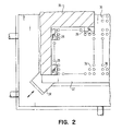
- FIGS. 1 and 2 serves to determine the exact location of each pattern 36 of connection contacts or soldering points on the substrate, with selected individual connection contacts or soldering points serving as reference points.
- the scanning probes 24, 26 and 28 attached to the scanning head 30 can be moved in the Z direction in engagement with or out of engagement with the patterns 36 from connection contacts or soldering support points on the substrate 32.
- the position of the substrate 32 can be adjusted by means of the servo control 22 in such a way that other patterns 36 of connection contacts or soldering points located on the substrate are located under the scanning head.
- the probes When the probe is moved down to contact the probes with the patterns of contacts or solder pads, the probes provide an accurate indication of the location of the reference points on the pattern 36, which contact subsequently makes an electrically conductive connection with the contacts or soldering points can be used by a scanning probe, so that the tests required to check the internal line connection of the substrate can be carried out. This information is then saved and can be used at a later time.
- the scanning probe consists of a base plate 40, in which can be clamped a number of leaf spring elements 42 in the bent state.
- the leaf spring element 42 shown in FIG. 3 has a central section 44, a contact section 46 and a connecting part 48. Stop faces 50 and 52 are provided on each side of the middle section 44.
- the leaf spring element 42 has a major axis 43 and a secondary axis 45.
- the leaf spring elements 42 are on their surface, with the exception of the contact surface 55 and the part 56 which is to be connected to a line 57, with a coating 54 made of a dielectric material, preferably of tetrafluoroethylene overdrawn.
- the leaf spring elements 42 are relatively thin, so that at least two of them will touch the terminal contact or the soldering base.
- the thickness of the leaf spring elements is in the range between 0.03 and 0.08 mm, while the thickness of the insulating coating 54 is in the range of 0.03 and 0.013 mm.
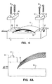
- the leaf spring elements 42 rest on the base plate 40 such that the central section is curved upwards, as shown, while the end sections 46 and 48 lie in a groove 47 and 49, respectively.
- each of the leaf spring elements is continuously slightly more curved than the previous one. This continuously greater curvature of the leaf spring elements is achieved in that an inwardly inclined stop surface 58 is provided, with which the stop surface 52 of the leaf spring elements 42 comes into engagement.
- leaf spring elements of the scanning probe are curved in the manner shown in FIG. 4, so that a limited mobility of the contact sections 46 of the individual leaf spring elements is possible. This allows a limited adaptation to an irregular surface.
- leaf spring members 42C, 42D, and 42E contact terminal 37. If leaf spring member 42D, which contacts the tip of terminal contact 37, were rigid, it would not be possible for the other two to close Leaf spring elements lying on both sides touch the connection contact. Furthermore, due to the progressively greater curvature of the individual elements due to the beveled surface 58 in FIG. 4, a certain flexibility is obtained for the leaf spring elements lying therebetween even when the adjacent leaf spring elements are in their original stretched position.
- a scanning probe which is however not shown, could consist, for example, of a number of leaf spring elements which are insulated from one another by a thin insulating coating and are individually clamped on one side.
- the leaf spring elements clamped on one side are thin L-shaped bent leaf springs, which are clamped in such a way that any deflection required for adaptation to a connection contact is absorbed by a slight bending of the leg of the clamped leaf spring element.
- the long or large portions of the leaf spring elements are held close to each other parallel to each other, corresponding to the end portions 46 of the leaf spring elements 42.
- the individual successive leaf spring elements can each be provided with a slightly longer leg, so that there is a slight distance that for a deflection of individual leaf spring elements is sufficient.
- the leg sections are fixed in a suitable manner so that the end sections of the leaf spring elements, which sense a connection contact or the like, are arranged in a plane parallel to the plane of the upper side of the substrate to be examined and tested.
- the sensing process of the sensing device according to FIG. 1 is initiated by lowering the scanning head 30 above the substrate 32, which contains a pattern 36 of connection contacts or soldering support points.
- the scanning probes 24, 26 and 28 are arranged on the scanning head 30 and are intended to determine predetermined connection contacts of the pattern which are to be used as reference points when determining the exact location of the pattern of connection contacts.
- the substrate 32 is attached beneath the scanning head 30 approximately to the desired location so that the scanning probes touch the connection contacts which serve as reference points.
- the contacts 37 which normally protrude slightly above the surface of the substrate, are contacted by two or more leaf spring elements 42. As shown in Fig.
- leaf spring elements 42C, 42D and 42E contact terminal 37, thereby shorting these three leaf spring elements together.
- This can be determined by a corresponding circuit, which is not shown here, since the leaf spring elements are provided with connecting lines 57A to 57G, which are connected to this circuit.
- Which leaf spring elements are short-circuited depends, of course, on the location of the connection contact37.
- a connection contact 37A is shown in Fig. 2A, which briefly the leaf spring elements 42C, 42D and 42E closes.
- the connection contact 37B short-circuits the leaf spring elements 42A, 42B and 42C in the position shown.
- connection contacts and the thickness or thickness of the leaf spring elements determines the number of leaf spring elements that are short-circuited by a connection contact. The location and number of leaf spring elements that are short-circuited together are determined, and this information is recorded either manually or via a program by a data processing system.
- the probe 24 can determine the precise location of a pattern of contacts with respect to the X direction, the probe 26 then determines the exact location of a pattern of contacts in the Y direction, and the probe 28 serves in conjunction with the Scanning probe 24 for determining the angular position of the pattern of connecting contacts.
- the leaf spring elements 42 are arranged so that the minor axis 45 is perpendicular to the X direction.
- the leaf spring elements 42 are arranged so that their minor axis 45 is perpendicular to the Y direction.
- the scanning probe 28 is arranged such that its leaf spring elements 42 are perpendicular to the X direction.
- the information determined by the short-circuited leaf spring elements enables, in conjunction with the reference point of the scanning probe, an exact determination of the location of a pattern of connection contacts on the substrate with only one pass.
- the substrate is then moved and the scanning head 30 is again moved down over a second pattern 36 of contacts, whereupon the process is repeated. In this way, information about the exact location of all patterns of connection contacts or soldering points on the substrate can be obtained.
- the locations of spaced connector patterns can be determined, and the location of the intermediate connector patterns can be approximated based on the precisely determined locations of the patterns by interpolation.
- the scanning head 30 can be lifted, after which test probes can establish an electrically conductive connection according to the individual patterns consisting of contact contacts, with a step-wise movement over the substrate in order to carry out the necessary tests.
- the servomotors 12, 14 and 16 can be used to drive the table 10 carrying the substrate 32 and to adjust the table with respect to the test probe, so that an electrically conductive connection is established with each connection contact.
- the substrate 32 is first placed below the scanning head so that the probes 24, 26 and 28 are likely to come into contact with the correct reference points of the patterns 36.
- the wrong reference points lie under the scanning probes can be the case if the distortion is exceptionally high. If, for example, the reference points are in the outer row and the scanning probes do not find the pattern in one direction, so that scanning probes lie outside the pattern, this state can be determined and the corresponding corrections can be carried out. If the same substrate is used both for testing and for determining the location of the pattern of connection contacts, then corresponding contact connections are made after connection pins 38 on the underside of substrate 32 for testing. However, the determination of the pattern of connection contacts does not require any contact to the circuit in the substrate, since the device and its work depend exclusively on a short circuit between adjacent leaf spring elements. The system can also be modified.
- the substrate can be set in the X and Y directions, and the scan head 30 can be moved from the location of one terminal to the location of the next terminal, if desired.
- the scanning probe can also be used for other purposes, i.e. H. to determine whether there are cable runs or cable patterns or not.
Landscapes
- Engineering & Computer Science (AREA)
- Physics & Mathematics (AREA)
- General Physics & Mathematics (AREA)
- Computer Hardware Design (AREA)
- Microelectronics & Electronic Packaging (AREA)
- General Engineering & Computer Science (AREA)
- Testing Of Short-Circuits, Discontinuities, Leakage, Or Incorrect Line Connections (AREA)
- Testing Or Measuring Of Semiconductors Or The Like (AREA)
- Measuring Leads Or Probes (AREA)
Applications Claiming Priority (2)
| Application Number | Priority Date | Filing Date | Title |
|---|---|---|---|
| US05/910,253 US4227149A (en) | 1978-05-30 | 1978-05-30 | Sensing probe for determining location of conductive features |
| US910253 | 1978-05-30 |
Publications (2)
| Publication Number | Publication Date |
|---|---|
| EP0005727A1 EP0005727A1 (de) | 1979-12-12 |
| EP0005727B1 true EP0005727B1 (de) | 1981-01-21 |
Family
ID=25428529
Family Applications (1)
| Application Number | Title | Priority Date | Filing Date |
|---|---|---|---|
| EP79101266A Expired EP0005727B1 (de) | 1978-05-30 | 1979-04-26 | Abfühlvorrichtung zum Feststellen des Ortes von elektrisch leitenden Punkten |
Country Status (4)
| Country | Link |
|---|---|
| US (1) | US4227149A (enExample) |
| EP (1) | EP0005727B1 (enExample) |
| JP (1) | JPS54157084A (enExample) |
| DE (1) | DE2960084D1 (enExample) |
Families Citing this family (14)
| Publication number | Priority date | Publication date | Assignee | Title |
|---|---|---|---|---|
| GB2034122B (en) * | 1978-10-02 | 1982-11-24 | British Gas Corp | Magnet assemblies for pipeline inspection vehicles |
| US4471298A (en) * | 1981-12-11 | 1984-09-11 | Cirdyne, Inc. | Apparatus for automatically electrically testing printed circuit boards |
| US4646009A (en) * | 1982-05-18 | 1987-02-24 | Ade Corporation | Contacts for conductivity-type sensors |
| US4810956A (en) * | 1987-12-21 | 1989-03-07 | Northern Telecom Limited | Mounting bracket for test probes |
| US5257024A (en) * | 1988-05-26 | 1993-10-26 | Quan-Scan, Inc. | Search position encoder |
| US5091693A (en) * | 1990-07-13 | 1992-02-25 | Schlumberger Technologies, Inc. | Dual-sided test head having floating contact surfaces |
| FR2670298B1 (fr) * | 1990-12-10 | 1993-03-05 | Aerospatiale | Systeme pour tester la continuite electrique et l'isolement des conducteurs electriques d'une piece de cablage. |
| US5597317A (en) * | 1995-08-11 | 1997-01-28 | W. L. Gore & Associates, Inc. | Surface mating electrical connector |
| CN1258212C (zh) * | 2001-04-04 | 2006-05-31 | 富士通株式会社 | 半导体器件用连接器装置以及半导体器件的测试方法 |
| US7128034B2 (en) | 2002-10-18 | 2006-10-31 | Maclean-Fogg Company | Valve lifter body |
| US7273026B2 (en) | 2002-10-18 | 2007-09-25 | Maclean-Fogg Company | Roller follower body |
| US6871622B2 (en) | 2002-10-18 | 2005-03-29 | Maclean-Fogg Company | Leakdown plunger |
| US7191745B2 (en) | 2002-10-18 | 2007-03-20 | Maclean-Fogg Company | Valve operating assembly |
| US7028654B2 (en) | 2002-10-18 | 2006-04-18 | The Maclean-Fogg Company | Metering socket |
Family Cites Families (10)
| Publication number | Priority date | Publication date | Assignee | Title |
|---|---|---|---|---|
| US806800A (en) * | 1905-06-30 | 1905-12-12 | Fleming E Greathouse | Reel-carrier. |
| US2932015A (en) * | 1956-12-26 | 1960-04-05 | Kelsey Hayes Co | Locating fixture and method |
| US3611128A (en) * | 1968-07-26 | 1971-10-05 | Hitachi Ltd | Probe header for testing integrated circuits |
| US3676776A (en) * | 1970-01-19 | 1972-07-11 | Siemens Ag | Testing probe construction |
| US3806801A (en) * | 1972-12-26 | 1974-04-23 | Ibm | Probe contactor having buckling beam probes |
| DE2344239B2 (de) * | 1973-09-01 | 1977-11-03 | Luther, Erich, 3050 Wunstorf; Maelzer, Fritz; Maelzer, Martin; 7910 Reutti Post Neu-Ulm; Türkkan, Tamer, 3011 Laatzen | Kontaktvorrichtung zum anschliessen einer gedruckten schaltung an ein pruefgeraet |
| US4019015A (en) * | 1973-09-10 | 1977-04-19 | International Business Machines Corporation | Precision tool and workpiece positioning apparatus with ringout detection |
| US4063172A (en) * | 1976-06-01 | 1977-12-13 | International Business Machines Corporation | Multiple site, differential displacement, surface contacting assembly |
| US4052793A (en) * | 1976-10-04 | 1977-10-11 | International Business Machines Corporation | Method of obtaining proper probe alignment in a multiple contact environment |
| US4177425A (en) * | 1977-09-06 | 1979-12-04 | Seymour Lenz | Multiple contact electrical test probe assembly |
-
1978
- 1978-05-30 US US05/910,253 patent/US4227149A/en not_active Expired - Lifetime
-
1979
- 1979-04-16 JP JP4553079A patent/JPS54157084A/ja active Granted
- 1979-04-26 EP EP79101266A patent/EP0005727B1/de not_active Expired
- 1979-04-26 DE DE7979101266T patent/DE2960084D1/de not_active Expired
Also Published As
| Publication number | Publication date |
|---|---|
| EP0005727A1 (de) | 1979-12-12 |
| DE2960084D1 (en) | 1981-03-12 |
| JPS5538827B2 (enExample) | 1980-10-07 |
| JPS54157084A (en) | 1979-12-11 |
| US4227149A (en) | 1980-10-07 |
Similar Documents
| Publication | Publication Date | Title |
|---|---|---|
| EP0078339B1 (de) | Tastkopfanordnung für Leiterzugüberprüfung mit mindestens einem, eine Vielzahl von federnden Kontakten aufweisenden Tastkopf | |
| DE2360801C2 (de) | Schaltungsprüfeinrichtung für integrierte Schaltkreise auf Schichtschaltungsträgern | |
| DE69422259T2 (de) | Verbindungseinrichtung | |
| EP0005727B1 (de) | Abfühlvorrichtung zum Feststellen des Ortes von elektrisch leitenden Punkten | |
| EP0468153B1 (de) | Kontaktierungsvorrichtung für Prüfzwecke | |
| EP0470118B1 (de) | Prüfvorrichtung zum prüfen von elektrischen oder elektronischen prüflingen | |
| DE2858098C2 (de) | Vorrichtung zum Aufbringen von rechteckigen oder länglichen Chips auf eine Leiterplatte | |
| DE19515154A1 (de) | Tastkopf-Meßhantiergerät, Verfahren zum Prüfen integrierter Schaltungen und integrierter Schaltungsbaustein | |
| DE2319011A1 (de) | Verfahren zum eektrischen pruefen eines chips untereinander verbindenden leiternetzes auf einem substrat | |
| EP2376930A1 (de) | Verfahren zum prüfen von leiterplatten | |
| EP1098200A2 (de) | Nadelkarten-Justageeinrichtung zur Planarisierung von Nadelsätzen einer Nadelkarte | |
| DE2744299A1 (de) | Verfahren zum ausrichten einer reihe von sonden auf eine reihe von kontakten | |
| DE4433693A1 (de) | Chipwiderstand, Schaltung und Verfahren zur Stromerfassung, die diesen Chipwiderstand verwenden, sowie Verfahren zum Einstellen des Wertes dieses Chipwiderstandes | |
| DE2906041A1 (de) | Vierquadranten-detektoranordnung | |
| WO2002021893A2 (de) | Verfahren und vorrichtung zum prüfen von leiterplatten mit einem paralleltester | |
| DE2547323C3 (de) | Trägerplatte für wenigstens eine integrierte Halbleitershaltung | |
| DE69422258T2 (de) | Verbindungseinrichtung | |
| DE68914005T2 (de) | Leitende Muster für den elektrischen Test von Halbleiterbausteinen. | |
| DE4302509B4 (de) | Verfahren zur Prüfung von Schaltungskarten | |
| DE9004562U1 (de) | Prüfvorrichtung zum Prüfen von elektrischen oder elektronischen Prüflingen | |
| DE69431233T2 (de) | Bestimmung des Oberflächenisolationswiderstands von Leiterplatten | |
| DE69423288T2 (de) | Verfahren zur Ankopplung einer Prüfanordnung an einen elektrischen Baustein | |
| DE4406674A1 (de) | Verfahren zum Prüfen einer zu prüfenden Elektrodenplatte | |
| DE4109684C2 (de) | Kontaktierungsvorrichtung für Prüfzwecke | |
| DE1913258C3 (de) | Abfühleinrichtung zum Überprüfen der Bestückung von Bauelementträgern |
Legal Events
| Date | Code | Title | Description |
|---|---|---|---|
| PUAI | Public reference made under article 153(3) epc to a published international application that has entered the european phase |
Free format text: ORIGINAL CODE: 0009012 |
|
| AK | Designated contracting states |
Designated state(s): DE FR GB |
|
| 17P | Request for examination filed | ||
| GRAA | (expected) grant |
Free format text: ORIGINAL CODE: 0009210 |
|
| AK | Designated contracting states |
Designated state(s): DE FR GB |
|
| REF | Corresponds to: |
Ref document number: 2960084 Country of ref document: DE Date of ref document: 19810312 |
|
| PGFP | Annual fee paid to national office [announced via postgrant information from national office to epo] |
Ref country code: FR Payment date: 19890324 Year of fee payment: 11 |
|
| PGFP | Annual fee paid to national office [announced via postgrant information from national office to epo] |
Ref country code: GB Payment date: 19890331 Year of fee payment: 11 |
|
| PG25 | Lapsed in a contracting state [announced via postgrant information from national office to epo] |
Ref country code: GB Effective date: 19900426 |
|
| PGFP | Annual fee paid to national office [announced via postgrant information from national office to epo] |
Ref country code: DE Payment date: 19900427 Year of fee payment: 12 |
|
| PG25 | Lapsed in a contracting state [announced via postgrant information from national office to epo] |
Ref country code: FR Effective date: 19901228 |
|
| GBPC | Gb: european patent ceased through non-payment of renewal fee | ||
| REG | Reference to a national code |
Ref country code: FR Ref legal event code: ST |
|
| PG25 | Lapsed in a contracting state [announced via postgrant information from national office to epo] |
Ref country code: DE Effective date: 19920201 |
|
| PLBE | No opposition filed within time limit |
Free format text: ORIGINAL CODE: 0009261 |
|
| STAA | Information on the status of an ep patent application or granted ep patent |
Free format text: STATUS: NO OPPOSITION FILED WITHIN TIME LIMIT |