EP0002433B1 - Verfahren zum Herstellen von Silicium-Photoelementen - Google Patents
Verfahren zum Herstellen von Silicium-Photoelementen Download PDFInfo
- Publication number
- EP0002433B1 EP0002433B1 EP78100845A EP78100845A EP0002433B1 EP 0002433 B1 EP0002433 B1 EP 0002433B1 EP 78100845 A EP78100845 A EP 78100845A EP 78100845 A EP78100845 A EP 78100845A EP 0002433 B1 EP0002433 B1 EP 0002433B1
- Authority
- EP
- European Patent Office
- Prior art keywords
- layer
- silicon
- aluminium
- doped
- pyramids
- Prior art date
- Legal status (The legal status is an assumption and is not a legal conclusion. Google has not performed a legal analysis and makes no representation as to the accuracy of the status listed.)
- Expired
Links
- 238000000034 method Methods 0.000 title claims description 77
- XUIMIQQOPSSXEZ-UHFFFAOYSA-N Silicon Chemical compound [Si] XUIMIQQOPSSXEZ-UHFFFAOYSA-N 0.000 title claims description 60
- 229910052710 silicon Inorganic materials 0.000 title claims description 60
- 239000010703 silicon Substances 0.000 title claims description 60
- 230000008569 process Effects 0.000 title claims description 22
- 229910052782 aluminium Inorganic materials 0.000 claims description 32
- XAGFODPZIPBFFR-UHFFFAOYSA-N aluminium Chemical compound [Al] XAGFODPZIPBFFR-UHFFFAOYSA-N 0.000 claims description 32
- 238000010438 heat treatment Methods 0.000 claims description 24
- 238000004519 manufacturing process Methods 0.000 claims description 14
- 239000000758 substrate Substances 0.000 claims description 12
- 239000011248 coating agent Substances 0.000 claims description 10
- 238000000576 coating method Methods 0.000 claims description 10
- 229910052751 metal Inorganic materials 0.000 claims description 9
- 239000002184 metal Substances 0.000 claims description 9
- 229910021421 monocrystalline silicon Inorganic materials 0.000 claims description 7
- 229910000838 Al alloy Inorganic materials 0.000 claims description 6
- 238000004544 sputter deposition Methods 0.000 claims description 6
- 239000007858 starting material Substances 0.000 claims description 6
- 229910000831 Steel Inorganic materials 0.000 claims description 5
- 238000000151 deposition Methods 0.000 claims description 5
- 239000010959 steel Substances 0.000 claims description 5
- 230000008021 deposition Effects 0.000 claims description 4
- 229910045601 alloy Inorganic materials 0.000 claims description 3
- 239000000956 alloy Substances 0.000 claims description 3
- 239000006117 anti-reflective coating Substances 0.000 claims description 3
- 239000012298 atmosphere Substances 0.000 claims description 3
- 238000007639 printing Methods 0.000 claims description 3
- 239000004568 cement Substances 0.000 claims description 2
- 230000005496 eutectics Effects 0.000 claims description 2
- 239000004411 aluminium Substances 0.000 claims 9
- KMWBBMXGHHLDKL-UHFFFAOYSA-N [AlH3].[Si] Chemical compound [AlH3].[Si] KMWBBMXGHHLDKL-UHFFFAOYSA-N 0.000 claims 1
- 239000012300 argon atmosphere Substances 0.000 claims 1
- 239000004065 semiconductor Substances 0.000 description 14
- 229910021417 amorphous silicon Inorganic materials 0.000 description 9
- 238000005496 tempering Methods 0.000 description 9
- 125000004429 atom Chemical group 0.000 description 8
- 238000000137 annealing Methods 0.000 description 6
- 230000015572 biosynthetic process Effects 0.000 description 5
- PXHVJJICTQNCMI-UHFFFAOYSA-N Nickel Chemical compound [Ni] PXHVJJICTQNCMI-UHFFFAOYSA-N 0.000 description 4
- 239000013078 crystal Substances 0.000 description 4
- 238000009792 diffusion process Methods 0.000 description 4
- 239000013067 intermediate product Substances 0.000 description 4
- 239000002244 precipitate Substances 0.000 description 4
- 238000007740 vapor deposition Methods 0.000 description 4
- 238000000637 aluminium metallisation Methods 0.000 description 3
- 230000008901 benefit Effects 0.000 description 3
- 238000006243 chemical reaction Methods 0.000 description 3
- 238000005530 etching Methods 0.000 description 3
- 238000001465 metallisation Methods 0.000 description 3
- 230000004048 modification Effects 0.000 description 3
- 238000012986 modification Methods 0.000 description 3
- 239000000243 solution Substances 0.000 description 3
- XKRFYHLGVUSROY-UHFFFAOYSA-N Argon Chemical compound [Ar] XKRFYHLGVUSROY-UHFFFAOYSA-N 0.000 description 2
- 238000005275 alloying Methods 0.000 description 2
- CSDREXVUYHZDNP-UHFFFAOYSA-N alumanylidynesilicon Chemical compound [Al].[Si] CSDREXVUYHZDNP-UHFFFAOYSA-N 0.000 description 2
- 238000002425 crystallisation Methods 0.000 description 2
- 230000008025 crystallization Effects 0.000 description 2
- 230000008020 evaporation Effects 0.000 description 2
- 238000001704 evaporation Methods 0.000 description 2
- 239000010408 film Substances 0.000 description 2
- 235000015244 frankfurter Nutrition 0.000 description 2
- LQBJWKCYZGMFEV-UHFFFAOYSA-N lead tin Chemical compound [Sn].[Pb] LQBJWKCYZGMFEV-UHFFFAOYSA-N 0.000 description 2
- 230000007935 neutral effect Effects 0.000 description 2
- 229910052759 nickel Inorganic materials 0.000 description 2
- -1 silane Chemical class 0.000 description 2
- 229910000679 solder Inorganic materials 0.000 description 2
- 229910018125 Al-Si Inorganic materials 0.000 description 1
- 229910018520 Al—Si Inorganic materials 0.000 description 1
- BLRPTPMANUNPDV-UHFFFAOYSA-N Silane Chemical compound [SiH4] BLRPTPMANUNPDV-UHFFFAOYSA-N 0.000 description 1
- QCWXUUIWCKQGHC-UHFFFAOYSA-N Zirconium Chemical compound [Zr] QCWXUUIWCKQGHC-UHFFFAOYSA-N 0.000 description 1
- 238000010521 absorption reaction Methods 0.000 description 1
- 239000012670 alkaline solution Substances 0.000 description 1
- 230000003667 anti-reflective effect Effects 0.000 description 1
- 229910052786 argon Inorganic materials 0.000 description 1
- 230000004888 barrier function Effects 0.000 description 1
- 239000003795 chemical substances by application Substances 0.000 description 1
- 150000001875 compounds Chemical class 0.000 description 1
- 239000000356 contaminant Substances 0.000 description 1
- 230000006378 damage Effects 0.000 description 1
- 230000007423 decrease Effects 0.000 description 1
- 230000007547 defect Effects 0.000 description 1
- 238000005516 engineering process Methods 0.000 description 1
- 239000000374 eutectic mixture Substances 0.000 description 1
- 239000000463 material Substances 0.000 description 1
- 230000008018 melting Effects 0.000 description 1
- 238000002844 melting Methods 0.000 description 1
- 229910052987 metal hydride Inorganic materials 0.000 description 1
- 150000004681 metal hydrides Chemical class 0.000 description 1
- 238000005272 metallurgy Methods 0.000 description 1
- 125000004437 phosphorous atom Chemical group 0.000 description 1
- 238000007747 plating Methods 0.000 description 1
- 229910021420 polycrystalline silicon Inorganic materials 0.000 description 1
- 238000001556 precipitation Methods 0.000 description 1
- 238000007788 roughening Methods 0.000 description 1
- 239000004576 sand Substances 0.000 description 1
- 229910000077 silane Inorganic materials 0.000 description 1
- 150000003377 silicon compounds Chemical class 0.000 description 1
- 239000010409 thin film Substances 0.000 description 1
- 230000007704 transition Effects 0.000 description 1
- 238000007738 vacuum evaporation Methods 0.000 description 1
- 229910052726 zirconium Inorganic materials 0.000 description 1
Images

Classifications
-
- H—ELECTRICITY
- H10—SEMICONDUCTOR DEVICES; ELECTRIC SOLID-STATE DEVICES NOT OTHERWISE PROVIDED FOR
- H10F—INORGANIC SEMICONDUCTOR DEVICES SENSITIVE TO INFRARED RADIATION, LIGHT, ELECTROMAGNETIC RADIATION OF SHORTER WAVELENGTH OR CORPUSCULAR RADIATION
- H10F77/00—Constructional details of devices covered by this subclass
- H10F77/20—Electrodes
- H10F77/206—Electrodes for devices having potential barriers
- H10F77/211—Electrodes for devices having potential barriers for photovoltaic cells
-
- H—ELECTRICITY
- H10—SEMICONDUCTOR DEVICES; ELECTRIC SOLID-STATE DEVICES NOT OTHERWISE PROVIDED FOR
- H10F—INORGANIC SEMICONDUCTOR DEVICES SENSITIVE TO INFRARED RADIATION, LIGHT, ELECTROMAGNETIC RADIATION OF SHORTER WAVELENGTH OR CORPUSCULAR RADIATION
- H10F77/00—Constructional details of devices covered by this subclass
- H10F77/70—Surface textures, e.g. pyramid structures
- H10F77/703—Surface textures, e.g. pyramid structures of the semiconductor bodies, e.g. textured active layers
-
- Y—GENERAL TAGGING OF NEW TECHNOLOGICAL DEVELOPMENTS; GENERAL TAGGING OF CROSS-SECTIONAL TECHNOLOGIES SPANNING OVER SEVERAL SECTIONS OF THE IPC; TECHNICAL SUBJECTS COVERED BY FORMER USPC CROSS-REFERENCE ART COLLECTIONS [XRACs] AND DIGESTS
- Y02—TECHNOLOGIES OR APPLICATIONS FOR MITIGATION OR ADAPTATION AGAINST CLIMATE CHANGE
- Y02E—REDUCTION OF GREENHOUSE GAS [GHG] EMISSIONS, RELATED TO ENERGY GENERATION, TRANSMISSION OR DISTRIBUTION
- Y02E10/00—Energy generation through renewable energy sources
- Y02E10/50—Photovoltaic [PV] energy
-
- Y—GENERAL TAGGING OF NEW TECHNOLOGICAL DEVELOPMENTS; GENERAL TAGGING OF CROSS-SECTIONAL TECHNOLOGIES SPANNING OVER SEVERAL SECTIONS OF THE IPC; TECHNICAL SUBJECTS COVERED BY FORMER USPC CROSS-REFERENCE ART COLLECTIONS [XRACs] AND DIGESTS
- Y10—TECHNICAL SUBJECTS COVERED BY FORMER USPC
- Y10S—TECHNICAL SUBJECTS COVERED BY FORMER USPC CROSS-REFERENCE ART COLLECTIONS [XRACs] AND DIGESTS
- Y10S148/00—Metal treatment
- Y10S148/033—Diffusion of aluminum
-
- Y—GENERAL TAGGING OF NEW TECHNOLOGICAL DEVELOPMENTS; GENERAL TAGGING OF CROSS-SECTIONAL TECHNOLOGIES SPANNING OVER SEVERAL SECTIONS OF THE IPC; TECHNICAL SUBJECTS COVERED BY FORMER USPC CROSS-REFERENCE ART COLLECTIONS [XRACs] AND DIGESTS
- Y10—TECHNICAL SUBJECTS COVERED BY FORMER USPC
- Y10S—TECHNICAL SUBJECTS COVERED BY FORMER USPC CROSS-REFERENCE ART COLLECTIONS [XRACs] AND DIGESTS
- Y10S438/00—Semiconductor device manufacturing: process
- Y10S438/964—Roughened surface
Definitions
- the invention relates to a method as can be seen in the preamble of claim 1.
- the invention has for its object to provide a manufacturing method for solar cells, which has been significantly simplified compared to previously and can provide operationally reliable and extremely effective solar cells or photo elements in a very simple manner with much less effort.
- the contacts of the N-doped layer becomes particularly simple. If non-monocrystalline silicon is used, an N layer can first be produced, which then changes into an N layer. A typical N concentration would then be 10 20 foreign atoms / cm 3 , whereas a typical N concentration could have 5 x 10 15 foreign atoms / cm 3 .
- the aluminum layer initially applied is approximately 400 nm thick and the silicon layer deposited thereon should have a thickness of 200 nm.
- the heating temperature and heating time are advantageously selected so that the lowest possible PN transition occurs, down to 0.1 ⁇ m, measured from the surface.
- a heating temperature of more than 500 ° C with a heating time of 4 to 5 hours is also advantageous to use.
- z. B amorphous silicon deposited on a substrate surface, consisting in particular of steel, so that a few 10 ⁇ m thick, amorphous, N-doped Si layer is formed on this metal substrate surface. Then, as already mentioned, aluminum and silicon are applied.
- the annealing to form the pyramid network according to the invention is carried out in a neutral atmosphere, such as. B. Argon to exclude reactions.
- the comb-like counterelectrode can be formed from the Al coating remaining after the tempering with the aid of photolithographic and printing processes known per se, or else advantageously by applying a wax layer to the released Al thin film after tempering.
- the wax layer can consist of vacuum cement and is applied in the form of the desired comb electrode.
- the metal surface areas exposed after this wax layer is exposed are a solution consisting of H 3 P0 4 HN0 3 , HCl and H 2 0 in a volume ratio of 20: 10: 10: 60, so that the metal is etched underneath. The remaining wax becomes then removed using CHCl 3 .
- the cross-sectional sections shown in FIG. 1 of the intermediate products resulting from process steps A to G do not represent true-to-scale illustrations, so that there is therefore no proportional enlargement of the individual elements. However, the same elements of the individual cross-sectional sections each have the same reference numerals.
- the method according to the invention is based on a Si layer 2, which is either by a silicon wafer alone, as in the process on the right. Step A is shown, or, as in method step A, can be represented on the left by a layer 2 deposited on a substrate 1, expediently at the same time serving as one of the electrodes, as is evident from method step B.
- the Si layer 2 is formed by an N semiconductor which is normally doped, ie below 5 ⁇ 10 18 foreign atoms / cm 3 , but then the Si layer 2 before metallization according to the known methods for producing ohmic contacts with N --doped Si is used.
- N semiconductor normally doped, ie below 5 ⁇ 10 18 foreign atoms / cm 3
- Electroless Nickel Plating for Making Ohmic Contacts to Silicon on pages 226 to 230 describes a process in which nickel is made an alkaline solution is electrolessly deposited on a Si substrate with 5x10 15 phosphorus atoms / cm 3 in order to then carry out an annealing at 700 ° C. This gives, for example, a contact square sheet resistance of approximately 0.01 ⁇ .
- Ohmic contacts can also be applied to Si semiconductors using lead-tin solder and fusing by means of laser beams, as described in the journal "Soviet Physics Semiconductors", Volume 3, No. 11, May 1970, pages 1383 to 1385.
- the Si layer 2 itself can consist of a wide variety of Si modifications.
- Si modifications in the case of quasi-monocrystalline and polycrystalline structures, as is evident from US Pat. No. 4,019,195 and German Offenlegungsschrift No. 2363135, there is an extremely inexpensive starting material for the production of silicon solar cells, which in the case of production using the method according to the invention has been by orders of magnitude so far are cheaper.
- Amorphous silicon can also be applied according to the invention to form the Si layer 2. This can be done in a manner known per se by means of vapor deposition or sputtering in conventional apparatus. However, it is a prerequisite that a corresponding proportion of N foreign atoms is involved in this process, the concentration of which advantageously decreases from N + to N - doping in the direction of the pyramid-covered surface, so that the desired doping of the Si layer 2 is established can.
- One of the possible application methods can also be found in the above-mentioned article »Amorphous Silicon for Semiconductor Manufacturing « in the »Frankfurter Symposium « from September 28, 1977.
- amorphous silicon modification z. B. proceed as follows: According to A in the left side of FIG. 1 serves as the electrode, that is for the substrate 1 of the Si layer 2, for B. a steel plate. This steel substrate 1 is fed into a known cathode sputtering device in order to then sputter N-type silicon in the amorphous state as layer 2 with a thickness of a few 10 ⁇ m. The resulting N-type precipitate as the Si layer 2 is excellently suitable for applying the antireflection coating according to the invention in the form of the network of the Si pyramids 7 with simultaneous formation of the P zone 4 and the counter electrode 5.
- a semiconductor 2 provided with a metal electrode 1 is thus present.
- the aluminum-silicon coating according to process step C is then applied to this monocrystalline, quasi-monocrystalline, polycrystalline or amorphous semiconductor of the Si layer 2.
- This coating can be applied either as an alloy layer 42 or in the form of separate aluminum and silicon films 40, 41 Precipitate Si layer 2, which, as stated, can represent either a wafer or a layer applied to a substrate.
- it is possible to use either cathode sputtering or vapor deposition methods, as are well known in the relevant art in both Precipitation processes can advantageously use a silicon-rich aluminum alloy as the starting material.
- the proportion of silicon in the aluminum is 1 to 5 percent by weight, namely d he solubility of silicon in aluminum increases with increasing heating temperature
- Another possibility for vapor deposition of the coating deposit 42 on the Si layer 2 can be carried out in such a way that a special crucible is used for each of aluminum and silicon, with different heating rates corresponding to the solubility of silicon in aluminum then having to be taken into account with simultaneous heating.
- separate aluminum and silicon layers 41, 40 can also be applied to the Si layer 2, likewise using the two methods mentioned above, in which case, of course, only one crucible during the deposition one layer is effective.
- a 400 nm thick aluminum layer 41 is first advantageously applied to the Si layer 2 in order to then deposit the 200 nm thick silicon layer 40 on the aluminum layer 41. It should be emphasized at this point that aluminum can provide P foreign atoms in a silicon semiconductor.
- the tempering process follows, which in all cases takes place below the melting point of the eutectic mixture of aluminum / silicon (89: 11 percent by weight).
- Si pyramids 7 are deposited in the precipitate 4 on the Si layer 2 as a dense network, so that after the method step D has been completed, the semiconductor surface is densely covered with Si pyramids 7.
- a monocrystalline or quasi-monocrystalline Si layer 2 epitaxially applied, P-doped Si pyramids 7 result.
- the Si pyramids 7 are doped with P foreign atoms, but the Si Layer 2 is essentially unable to accept any Al atoms, since the diffusion temperature required for this, in conjunction with the diffusion duration likewise necessary, is not achieved when the method according to the invention is used.
- the tempering process according to process step D is therefore carried out below the eutectic temperatures Al-Si and takes place in a neutral atmosphere, but preferably in argon, in order to exclude undesired reactions.
- the heating temperature used for the annealing is decisive for the height of the Si pyramids 7 that are formed and for the depth of the PN junction 3. It can be seen that at a relatively high heating temperature the rate of crystallization is correspondingly higher, so that lower Si pyramids 7 due to the formation of relatively small crystals, and the PN junction 3 also comes to a greater depth. It should be noted, however, that the duration of the annealing process can also have some influence. Accordingly, larger Si pyramids 7 form at a relatively low temperature, but then the PN junction then also has to be flatter; but, as already mentioned, can be lowered by a correspondingly longer annealing time. So z. B.
- the heating temperature is 500 ° C., as in the exemplary embodiment mentioned with a 400 nm thick aluminum layer 41 on the Si layer 2 and with an aluminum layer 41 on this in a thickness of 200 nm applied Si layer 40.
- the aluminum proportion should be chosen so large that the thickness of the aluminum layer 5 resulting after application of the tempering process in method step D is such that the electrical resistance in this aluminum layer 5 for use as silicon Is sufficiently low. It must of course be taken into account here that this aluminum layer 5 still has to be etched out to form a comb-like electrode 50 using method steps E to G. Since, in addition to the resistance in the P zone 4, the electrode resistance is of considerable importance for the efficiency of a silicon photoelement, adequate attention must also be paid to this point.
- the heating temperature during tempering in process step D is very decisive for the height of the Si pyramids 7 formed on the Si layer 2 and for the depth of the PN junction 3.
- the rate of crystallization also increases, so that lower Si pyramids 7 form on the surface of the Si layer 2, since smaller crystals are formed in the process.
- the depth of the PN junction 3 increases with the heating temperature, the duration of the tempering process also playing a role, of course, since the PN junction 3 comes to be correspondingly lower with a longer heating time. If the heating temperature is not so high during tempering, then correspondingly larger crystals form on the surface of the Si layer 2, the PN junction 3 simultaneously being correspondingly flatter. However, as said, this PN junction 3 can be lowered by increasing the heating time accordingly.
- the PN junction When using a monocrystal as the Si layer 2, the PN junction should be as deep as possible, namely up to about 0.1 flm, measured from the surface.
- the resulting intermediate product accordingly contains an N-doped Si layer 2, which is coated with a layer 4 containing P-doped Si pyramids 7 on its surface facing away from the electrode 1 in the form of a dense network, the Si pyramids 7 in turn are covered with an aluminum metallization 5, which, as mentioned, is applied in the thickness required for the application and is used to represent the counterelectrode by means of process steps E to G.
- the Si pyramids 7 on the surface of the Si layer 2 result in a density sufficient for the antireflectivity if silicon is provided in an appropriate amount for process step C.
- the Si pyramids 7 are microscopically small, the antireflectivity of the layer 4 is large enough and therefore sufficiently effective, since with high density of the Si pyramids 7 light rays incident on the surface of the Si layer 2 upon reflection on other Si pyramids 7 are steered and thus cannot be radiated outwards again.
- an additional increase in efficiency is brought about by internal multiple reflections of the longer-wave light between the back and front of the silicon photoelement.
- a method which is particularly advantageous for the silicon photoelement to be produced according to the invention consists in that a wax layer 10, for. B. vacuum putty, is applied in the form of the desired comb electrode 50 (process step F). Then, in continuation of process step F, the free surface of the aluminum metallization 5 is exposed to an etching solution which is made up of H 3 P0 4 , HN0 3 , HCl and H 2 0 in a volume ratio of 20: 10: 10: 60, so that can etch the aluminum metallization 5 in the desired manner.
- Si pyramids 7 previously covered are exposed when using method step G and the wax still present on the resulting comb electrode 50 is finally detached by means of a CHCI 3 solution.
- the comb electrode 50 thus formed forms the positive pole of the silicon photoelement produced according to the invention, the negative pole of which is represented by the metal electrode 1 which has already been attached.
- the PN junction 3, the metallization of the counterelectrode 50 and the antireflection layer 4 are formed in only two process steps when producing a silicon photoelement
- the advantage of the invention is obvious. This advantage is further increased by the fact that the PN junction 3 required for the provision of a photo element does not have to be subsequently introduced into the Si semiconductor, but rather automatically occurs when the Si pyramids 7 are formed.
Landscapes
- Photovoltaic Devices (AREA)
- Electrodes Of Semiconductors (AREA)
Description
- Die Erfindung betrifft em Verfahren, wie es dem Oberbegriff des Fatentanspruchs 1 zu entnehmen ist.
- Zur Herstellung von Silicium Photoelementen, insbesondere Sonnenzelien, sind bisher eine große Anzahl von Verfahrensschritten erforderlich, so daß allein schon hieraus ein erheblicher Herstellungsaufwand unabläßlich erscheint. Hierbei muß zunächst ein geeigneter Si-Wafer einer Diffusion zur Bildung eines PN-Überganges unterworfen werden, anschließend eine antireflektierende Schicht entweder durch Oberflä chenzerstörung oder Aufdampfen besonderer Schichten bereitgestellt werden, um anschließend die Elektrodenmetallisierung anzubringen, wovon dann die eine abschließend in üblicher Weise als Kammelektrode ausgebildet wird. Das Absorptionsvermögen und damit der Wirkungsgrad derartig hergestellter Sonnenzellen läßt sich erheblich verbessern, wenn, wie bereits in der deutschen Offenlegungsschrift 1 621 511 beschrieben. die bestrahlte Oberfläche mit einem dichten Netzwerk von Si-Pyramiden überzogen wird Dies laßt sich durchführen, indem eine Silicium-Monokristall-Oberfläche in (100)-Richtung angeätzt wird, so daß dann nach diesem Ätzvorgang Silicium-Pyramiden mit ihren (111)-Flanken auf der Oberfläche verbleiben. Nachteilig hierbei ist es, daß der PN-Übergang nachher hergestellt werden muß und daß das Ausgangsmaterial, nämlich die Silicium-Monokristallschicht, relativ teuer ist. Wenn auch als Ersatz nicht-monokristallines Silicium, jedoch überhaupt nicht polyknstallines Silicium, Anwendung finden kann, so ist dann noch von der Tatsache nicht abzusehen, daß die Herstellung eines derartigen Grundmaterials immerhin noch einen gewissen Aufwand erfordert und damit nicht ganz einfach ist
- Andererseits ist zwar die Verwendung von polykristallinem und amorphen Silicium für Sonnenzellen an sich bekannt, jedoch ergeben sich für das Anbringen der Elektroden und des Aufbringens von Antireflexbelägen, insbesondere aber für das Erzeugen eines flachen PN-Übergangs, nicht unwesentliche Schwierigkeiten. Eine Zusammenfassung über Sonnenzellen üblicher Bauart findet sich in der Zeitschrift »Umschau« Band 77 (1977), Heft 13, unter dem Titel »Elektrische Energie von der Sonne«, Seiten 421 bis 427.
- Demgegenüber liegt der Erfindung die Aufgabe zugrunde, ein Herstellungsverfahren für Sonnenzellen bereitzustellen, das gegenüber bisher wesentlich vereinfacht ist und bei sehr viel geringerem Aufwand betriebszuverlässige und äußerst wirksame Sonnenzellen bzw. Photoelemente in einfachster Weise bereitzustellen vermag.
-

- Wenn es auch für das Erreichen eines hohen Wirkungsgrades der Sonnenzelle von besonde rem Vorteil ist, von einer niedrig doberten Si-Lage auszugehen, läßt sich andererseits auch eine Dotierung oberhalb von 5 x 10¹⁸ Fremdato men pro cm3 anwenden, wobei die Kontakte rung der N-dotierten Lage besonders einfach wird. Bei Verwendung von nicht-monokristallinem Silicium kann erst eine N--Schicht, die dann in eine N--Schicht übergeht, erzeugt werden. Eine typische N-Konzentration wäre dann 1020 Fremdatome/cm3, wohingegen eine typische N--Konzentration 5 x 10¹⁵Fremdato me/cm3 aufweisen könnte.
- Zur Durchführung der erfindungsgemäßen Verfahrensschritte ergeben sich verschiedene Möglichkeiten, nämlich einmal mit Hilfe der Kathodenzerstäubung aus einer siliciumreichen Aluminiumlegierung als Target die Si-Lage entsprechend zubeschichten oder Aluminium oder Silicium auf die Si-Lage mittels Vakuumbeuampfung aufzutragen. Bei beiden Verfahrensschritte dient in vorteilhafter Weise eine Legierung als Ausgangsmaterial, bei der 1 bis 5 Gewichtsprozent von in Aluminium gelöstem Silicium unter Berücksichtigung der maximalen Siliciumlöslichkert bei der verwendeten Aufheiztemperatur gewänlt wird. Bei Verwendung getrennter Tiegel tur Aluminium und Silicium müssen bei gleichzeitiger Beheizung entsprechend unterschiedliche Aufdampfraten für Aluminium und Silicium angewendet werden.
- Andererseits ist es auch möglich, die Erfindung durchzuführen, indem getrennte Schichten von Aluminium und Silicium auf die Si-Lage aufgebracht werden. In vorteilhafter Weise ist dabei die zunächst aufgetragene Aluminium- schicht etwa 400 nm dick und die hierauf niedergeschlagene Siliciumschicht sollte eine Dicke von 200 nm aufweisen.
- Bei Verwendung einer monokristallinen Si-Lage werden vorteilhafter Weise Aufheiztemperatur und Aufheizdauer so gewählt, daß sich ein möglichst tiefer PN-Übergang einstellt, und zwar bis auf 0,1 µm, gemessen von der Oberfläche. Bei Verwendung von korngrenzfreien, monokristallinen Si-Lagen ist es weiterhin von Vorteil, eine Aufheiztemperatur von mehr als 500°C bei einer Aufheizdauer von 4 bis 5 Stunden Dauer anzuwenden.
- Dank der Vorteile des erfindungsgemäßen Verfahrens ist es auch ohne weiteres möglich, nicht-monokristallines Silicium als Si-Lage zu verwenden. Selbstverständlich gilt entsprechendes auch für eine Si-Lage, die mit Korngrenzen durchzogen ist In vorteilhafter Ausgestaltung der Erfindung wird hierbei z. B. amorphes Silicium auf eine Substratoberfläche, bestehend insbesondere aus Stahl, niedergeschlagen, so daß sich eine einige 10µm dicke, amorphe, N-dotierte Si-Lage auf dieser Metallsubstratoberfläche bildet. Hierauf erfolgt dann, wie bereits erwähnt, das Auftragen von Aluminium und Silicium.
- Zur Bildung der amorphen Si-Lage lassen sich verschiedene Verfahren anwenden, die an sich bekannt sind, nämlich einmal Kathodenzerstäubung und zum anderen Reaktionsniederschlag, wie in der »Frankfurter Zeitung« vom 28. 09. 1977 unter dem Titel »Amorphes Silicium für die Halbleiterfertigung« angegeben; wo von einer gasförmigen Siliciumverbindung, nämlich Silan, ausgegangen wird, das in einer elektrischen Entladung disoziiert wird, so daß sich auf einem geheizten Substrat ein amorpher Siliciumfilm ausbilden kann.
- Allgemein wird die Temperung zur Bildung des Pyramidennetzwerks gemäß der Erfindung in neutraler Atmosphäre durchgeführt, wie z. B. Argon, um Reaktionen auszuschließen.
- Die Ausbildung der kammartigen Gegenelektrode aus der nach der Temperung verbleibenden AI-Beschichtung kann mit Hilfe an sich bekannter photolithographischer und drucktechnischer Verfahren erfolgen oder aber auch in vorteilhafter Weise durch Auftragen einei Wachsschicht auf den freigesetzten Al-Dünnfirm nach Temperung. Die Wachsschicht kann aus Vakuumkitt bestehen und wird in Form der gewünschten Kammelektrode aufgebracht. Die nach Aufbringen dieser Wachsschicht freible benden Metalloberflächenbereiche werden ei ner Lösung, bestehend aus H3P04HN03, HCI und H20 im Volumenverhältnis 20 : 10 : 10 : 60 ausge setzt, so daß das Metall hierunter abgeätzt wird Das verbliebene Wachs wird dann anschließend mittels CHCl3abgelöst.
- Wie ersichtlich, wird also, dank der Erfindung, ein relativ einfaches Herstellungsverfahren für photoelektrische Elemente, bestehend aus Silicium, bereitgestellt, welches in seinen Verfab rensschritten eines wesentlich geringeren Aufwandes bedarf als es bei bisher üblichen Verfahren der Fall ist. Dadurch, daß die gewählte Aufheiztemperatur relativ gering ist, ergibt s'ch keine Diffusion von A1 in die Si-Lage entlang der Korngrenzen, so daß hierfür ohne weiteres amorphes, polykristallines und auch quasi-mcnokristallines Silicium Verwendung finden kann.
- Die Erfindung wird anschließend anhand einer Ausführungsbeispielsbeschreibung mit Hilfe der unten aufgeführten Zeichnungen näher erläutert.
- Es zeigt
- Fig. 1A-1G Querschnittsausschnitte des sich bei den einzelnen Verfahrensschritten jeweils ergebenden Zwischenproduktes in der Herstellung des Silicium-Photoelements gemäß der Erfindung,
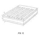
- Fig 2 eine perspektivische, schematische Ansicht des erfindungsgemäß fertiggestellten Silicium-Photoelements.
- Die in Fig. 1 dargestellten Querschnittsausschnitte der sich bei den Verfahrensschritten A bis G ergebenden Zwischenprodukte stellen keine maßstäblich genauen Abbildungen dar, so daß also keine proportionale Vergrößerung der einzelnen Elemente vorliegt. Gleiche Elemente der einzelnen Querschnittsausschnitte besitzen jedoch jeweils gleiches Bezugszeichen Das erfindungsgemäße Verfahren geht dabei von einer Si-Lage 2 aus, die entweder durch einen Silicium-Wafer allein, wie rechts beim Verfah. rensschritt A gezeigt, oder wie beim Verfahrensschritt A, links durch eine auf einem, zweckmäßigerweise gleichzeitig als eine der Elektroden dienendem Substrat 1 niedergeschlagenen Schicht 2 dargestellt werden kann, wie es sich aus Verfahrensschritt B ergibt. Die Si-Lage 2 wird durch einen N-Halbleiter gebildet, der normal dotiert ist, d. h. unterhalb von 5 x 10¹⁸ Fremdatomen/cm3, wobei dann allerdings vor Metallisierung die Si-Lage 2 nach den bekannten Methoden zur Herstellung ohmscher Kontakte mit N--dotiertem Si Anwendung findet. So ist z. B. in »Journal of the Electrochemical Society Band 104, Nr.4, April 1957 unter dem Titel »Electroless Nickel Plating for Making Ohmic Contacts to Silicon« auf den Seiten 226 bis 230 ein Verfahren beschrieben, bei dem Nickel aus einer alkalischen Lösung stromlos auf ein Si-Substrat mit 5x10¹⁵ Phosphoratomen/cm3 ausgeschieden wird, um dann eine Temperung bei 700°C durchzuführen. Hierbei ergibt sich beispielsweise ein Kontakt-Quadratflächenwiderstand von ca. 0,01 Ω.
- In einer weiteren Veröffentlichung in der gleichen Zeitschrift, Band 103, Nr.4, April 1956 unter dem Titel »Five Metal Hydrides as Alloying Agents on Silicon«, auf den Seiten 218 bis 220 zeigt sich eine Methode zum Kontaktieren von N--dotiertem Silicium durch Beschleunigung des Legierungsvorgangs von Blei-Zinnlot mit Hilfe von Zirkon- und Titanhydriden. Typische Kontaktwiderstände von 0,001 Ω/cm2 lassen sich hierbei erreichen.
- Ebenfalls unter Anwenden von Blei-Zinnlot und Verschmelzen mittels Laserstrahlen lassen sich ohmsche Kontakte auf Si-Halbleitern aufbringen, wie es in der Zeitschrift »Soviet Physics Semiconductors«, Band 3, Nr. 11, Mai 1970, Seiten 1383 bis 1385 beschrieben ist.
- Schließlich ist im Buch von Lindmayer-Wrigley »Fundamental of Semiconductor Devices«, auf den Seiten 358 und 359 die Bildung ohmscher Kontakte durch Hervorrufen hoher Defektdichten mittels mechanischem Aufrauhens der Kristalloberfläche, z. B. Sandblasen, angegeben. In allen Fällen ergibt sich, daß die Ausbildung einer Schottky-Sperrschicht verhindert wird, die andererseits bei Betrieb des erfindungsgemäß hergestellten Silicium-Photoelements den Wirkungsgrad nicht unwesentlich beeinträchtigen würde.
- Die Si-Lage 2 selbst kann aus den verschiedensten Si-Modifikationen bestehen. Bei quasimonokristalliner und bei polykristalliner Struktur, wie es sich aus der US-Patentschrift 4019195 und aus der deutschen Offenlegungsschrift 2363135 ergibt, liegt ein äußerst günstiges Ausgangsmaterial für die Herstellung von Silicium-Sonnenzellen vor, die bei Herstellung unter Anwendung des erfindungsgemäßen Verfahrens gegenüber bisher um Größenordnungen billiger sind.
- Mit Si-Pyramiden übersäte Halbleiteroberflächen als solche lassen sich durch epitaxiales Wachstum von 150-300 µm dichten Schichten, wie im Buch »Metallurgial Society Conferences«, Bd. 12, unter dem Titel »Metallurgy of Elemental and Compounds Semiconductors« auf den Seiten 246, 247, erschienen bei »Intercience Publishers«, New York/London 1961, angegeben, herstellen. Derartige Strukturen lassen sich aber nicht als Solarzellen anwenden, da die Ausbildung eines PN-Übergangs in definierter Tiefe nicht in einem und demselben Verfahrensgang bereitgestellt werden kann.
- Auch amorphes Silicium läßt sich gemäß der Erfindung zur Ausbildung der Si-Lage 2 auftragen. Dies kann in an sich bekannter Weise mittels Aufdampfen oder Kathodenzerstäuben in gebräuchlichen Apparaturen erfolgen. Voraussetzung ist allerdings, daß bei diesem Vorgang ein entsprechender Anteil an N-Fremdatomen beteiligt ist, deren Konzentration in vorteilhafter Weise von N+- zur N--Dotierung in Richtung zur pyramidenbesetzten Oberfläche abnimmt, damit sich die gewünschte Dotierung der Si-Lage 2 einstellen kann. Eines der möglichen Auftragungsverfahren ist auch dem obengenannten Artikel »Amorphes Silicium für die Halbleiterfertigung« in der »Frankfurter Zeitung« vom 28.09.1977 zu entnehmen. Es bleibt jedoch festzuhalten, daß bei allen anwendbaren Verfahren zum Niederschlag einer amorphen Si-Lage 2 die in vorgegebener Weise mit N-Fremdatomen dotiert ist, keinerlei Schwierigkeiten bei der Fertigstellung des Silicium-Photoelements auftreten, da bei Anwendung des erfindungsgemäßen Verfahrens nach Aufbringen der Si-Lage 2 auf das jeweilige Substrat 1 bzw. nach entsprechender Behandlung des Wafers hierin kein PN-Übergang mehr eingebracht zu werden braucht. Jedenfalls kann ein Metallsubstrat 1 der Si-Lage 2 gleichzeitig als negative Elektrode des herzustellenden Silicium-Photoelements dienen.
- Bei Verwendung einer amorphen Silicium-Modifikation läßt sich z. B. wie folgt verfahren: Gemäß A in der linken Seite der Fig. 1 dient als Elektrode, also für das Substrat 1 der Si-Lage 2, z. B. ein Stahlplättchen. Dieses Stahlsubstrat 1 wird in eine bekannte Kathodenzerstäubungseinrichtung eingegeben, um hierauf N-leitendes Silicium im amorphen Zustand als Lage 2 in einer Dicke von einigen 10 µm aufzustäuben. Der sich ergebende N-leitende Niederschlag als Si-Lage 2 ist in hervorragender Weise für das Aufbringen des Antireflexbelages gemäß der Erfindung in Form des Netzwerks der Si-Pyramiden 7 unter gleichzeitiger Bildung der P-Zone 4 und der Gegenelektrode 5 geeignet.
- Nach Abschluß des Verfahrensschrittes B liegt also ein mit einer Metallelektrode 1 versehener Halbleiter 2 vor. Auf diesen monokristallinen, quasi-monokristallinen, polykristallinen oder amorphen Halbleiter der Si-Lage 2 wird anschließend die Aluminium-Siliciumbeschichtung gemäß dem Verfahrensschritt C aufgebracht Diese Beschichtung läßt sich entweder als Legierungsschicht 42 oder in Form jeweils getrennter Aluminium- und Siliciumfilme 40, 41 auf die Si-Lage 2 niederschlagen, die, wie gesagt, entweder ein Wafer oder eine auf einem Substrat aufgebrachte Schicht darstellen kann In anderen Fällen jedoch ist es möglich, hierzu entweder Kathodenzerstäubungs- oder Aufdampfverfahren anzuwenden, wie sie in der einschlägigen Technik durchaus bekannt sind Bei beiden Niederschlagsverfahren läßt sich in vorteilhafter Weise als Ausgangsmaterial eine siliciumreiche Aluminiumlegierung anwenden Je nach Höhe der Aufheiztemperatur, wie sie nach Aufbringen der siliciumreichen Aluminium- legierung auf die Si-Lage 2 Anwendung findet, beträgt der Anteil des Siliciums im Aluminium 1 bis 5 Gewichtsprozent, da nämlich die Löslich keit von Silicium in Aluminium mit steigender Aufheiztemperatur wächst
- Wird ein Verdampfungsvorgang zum Bp schichtungsniederschlag angewendet, dann geschieht dies zweckmäßiger Weise im Vakuum, um das Eindringen von Verunreinigungen in den Beschichtungsniederschlag 42 von vornherein auszuschalten. Der Tiegel mit der hierin enthaltenen siliciumreichen Aluminiumlegierung wird also entsprechend beheizt, bis sich die Beschichtung 42 auf der Si-Lage 2 in ausreichender Dicke eingestellt hat.
- Eine andere Möglichkeit zum Aufdampfen des Beschichtungsniederschlags 42 auf die Si-Lage 2 läßt sich so durchführen, daß je für Aluminium und Silicium ein besonderer Tiegel verwendet wird, wobei dann bei gleichzeitiger Beheizung jeweils unterschiedliche Aufheizungsraten entsprechend der Löslichkeit von Silicium in Aluminium berücksichtigt werden müssen. Schließlich lassen sich auch, wie beim Verfahrensschritt C auf der linken Seite gezeigt, getrennte Aluminium- und Siliciumschichten 41, 40 auf die Si-Lage 2 aufbringen, und zwar ebenfalls unter Anwenden der beiden obengenannten Verfahren, wobei dann natürlich jeweils nur ein Tiegel beim Niederschlagen einer Schicht wirksam ist. Hierbei wird in vorteilhafter Weise zunächst eine 400 nm dicke Aluminium- schicht 41 auf die Si-Lage 2 aufgebracht, um anschließend die 200 nm dicke Siliciumschicht 40 auf die Aluminiumschicht 41 ihrerseits niederzuschlagen. Hervorzuheben ist an dieser Stelle, daß Aluminium in einem Siliciumhalbleiter P-Fremdatome bereitzustellen vermag.
- Nach Aufbringen der Silicium-Aluminium-Beschichtung 42 bzw. 40, 41 schließt sich erfindungsgemäß der Temperungsvorgang an, der in allen Fällen unterhalb des Schmelzpunktes des eutektischen Gemisches von Aluminium/Silicium (89 : 11 Gewichtsprozent) erfolgt. Bei diesem Temperungsvorgang (Verfahrensschritt D) setzen sich Si-Pyramiden 7 im Niederschlag 4 auf die Si-Lage 2 als dichtes Netzwerk ab, so daß nach Abschluß des Verfahrensschrittes D die Halbleiteroberfläche mit Si-Pyramiden 7 dicht übersät ist. Im Falle einer monokristallinen oder quasi-monokristallinen Si-Lage 2 ergeben sich epitaxial aufgetragene, P-dotierte Si-Pyramiden 7. Bedeutsam ist, daß bei diesem Vorgang zwar die Si-Pyramiden 7 mit P-Fremdatomen dotiert werden, jedoch die darunterliegende Si-Lage 2 im wesentlichen keine AI-Atome aufzunehmen vermag, da die hierzu erforderliche Diffusionstemperatur in Verbindung mit der ebenfalls notwendigen Diffusionsdauer bei Anwendung des erfindungsgemäßen Verfahrens nicht erreicht wird. Der Temperungsvorgang gemäß Verfahrensschritt D wird also unterhalb der eutektischen Temperaturen AI-Si durchgeführt und findet in neutraler Atmosphäre, vorzugsweise jedoch in Argon, statt, um unerwünschte Reaktionen auszuschließen.
- Die zur Temperung angewendete Aufheiztemperatur ist entscheidend für die Höhe der sich ausbildenden Si-Pyramiden 7 und für die Tiefe des PN-Übergangs 3. So zeigt sich, daß bei relativ hoher Aufheiztemperatur die Kristallisationsgeschwindigkeit entsprechend höher ist, so daß sich niedrigere Si-Pyramiden 7 aufgrund der Ausbildung relativ kleiner Kristalle ergeben, und dabei auch der PN-Übergang 3 in größere Tiefe zu liegen kommt. Zu berücksichtigen ist allerdings, daß außerdem auch die Temperungsdauer von gewissem Einfluß sein kann. Bei relativ niedriger Temperatur bilden sich dementsprechend größere Si-Pyramiden 7 aus, wobei dann jedoch der PN-Übergang auch flacher zu liegen kommt; aber, wie bereits erwähnt, durch entsprechend längere Temperungsdauer tiefer gelegt werden kann. So kann z. B. bei einer Temperungsdauer von 4 bis 5 Stunden die Aufheiztemperatur bei 500°C liegen, wie im angeführten Ausführungsbeispiel mit einer 400 nm dicken Aluminium-Schicht 41 auf der Si-Lage 2 und mit einer auf diese Aluminium- Schicht 41 in einer Dicke von 200 nm aufgetragenen Si-Schicht40.
- Im Ausgangsmaterial für die Beschichtung der Si-Lage 2 sollte der Aluminiumanteil so groß gewählt sein, daß die sich nach Anwendung des Temperungsvorganges im Verfahrensschritt D ergebende Dicke der Aluminiumschicht 5 derart einstellt, daß der elektrische Widerstand in dieser Aluminiumschicht 5 für die Anwendung als Silicium-Photoelement ausreichend niedrig ist. Hierbei muß natürlich berücksichtigt werden, daß diese Aluminiumschicht 5 ja noch zur Bildung einer kammartigen Elektrode 50 unter Anwenden der Verfahrensschritte E bis G ausgeätzt werden muß. Da neben dem Widerstand in der P-Zone 4 der Elektrodenwiderstand für den Wirkungsgrad eines Silicium-Photoelements von erheblicher Bedeutung ist, muß diesem Punkt entsprechend auch hinreichende Beachtung geschenkt werden.
- Zusammenfassend läßt sich sagen, daß die Aufheiztemperatur bei Temperung im Verfahrensschritt D für die Höhe der sich auf der Si-Lage 2 bildenden Si-Pyramiden 7 und für die Tiefe des PN-Übergangs 3 ganz entscheidend ist. Mit bei Temperung steigender Temperatur wächst auch die Kristallisationsgeschwindigkeit, so daß sich niedrigere Si-Pyramiden 7 auf der Oberfläche der Si-Lage 2 ausbilden, da hierbei kleinere Kristalle entstehen. Außerdem wächst die Tiefe des PN-Übergangs 3 mit der Aufheiztemperatur an, wobei natürlich auch die Dauer des Temperungsvorganges eine Rolle spielt, da bei längerer Aufheizdauer der PN-Übergang 3 entsprechend tiefer zu liegen kommt. Ist die Aufheiztemperatur bei Temperung nicht so hoch, dann bilden sich entsprechend größere Kristalle an der Oberfläche Si-Lage 2 aus, wobei sich gleichzeitig der PN-Übergang 3 entsprechend flacher einstellt. Jedoch kann, wie gesagt, durch entsprechendes Erhöhen der Aufheizdauer dieser PN-Übergang 3 tiefer gelegt werden.
- Bei Verwendung eines Monokristalls als Si-Lage 2 sollte der PN-Übergang so tief wie möglich liegen, nämlich bis etwa zu 0,1 flm, gemessen von der Oberfläche.
- Das sich nach Abschluß des Verfahrensschrittes D ergebende Zwischenprodukt enthält demnach eine N-dotierte Si-Lage 2, die mit einer P-dotierte Si-Pyramiden 7 enthaltenden Schicht 4 an ihrer, der Elektrode 1 abgewandten Fläche in Form eines dichten Netzes überzogen ist, wobei die Si-Pyramiden 7 ihrerseits hinwiederum mit einer Aluminium-Metallisierung 5 bedeckt sind, die, wie erwähnt, in für die Anwendungszwecke erforderlicher Dicke aufgebracht ist und zur Darstellung der Gegenelektrode mittels der Verfahrensschritte E bis G herangezogen wird.
- Die Si-Pyramiden 7 auf der Oberfläche der Si-Lage 2 ergeben sich in für das Antireflexionsvermögen ausreichender Dichte, wenn für den Verfahrensschritt C Silicium in entsprechender Menge vorgesehen wird. Obwohl die Si-Pyramiden 7 mikroskopisch klein sind, ist das Antireflexionsvermögen der Schicht 4 groß genug und damit hinreichend wirksam, da bei großer Dichte der Si-Pyramiden 7 auf der Oberfläche der Si-Lage 2 einfallende Lichtstrahlen bei Reflexion auf jeweils andere Si-Pyramiden 7 gelenkt werden und damit nicht wieder nach außen abgestrahlt werden können. Hinzu kommt, daß dank der mit den Si-Pyramiden 7 übersäten Oberfläche der Si-Lage 2 durch interne Mehrfachreflexionen des langwelligeren Lichtes zwischen Rück- und Vorderseite des Silicium-Photoelements eine zusätzliche Erhöhung des Wirkungsgrades herbeigeführt wird.
- Zur speziellen Ausbildung der Gegenelektrode 50 in kammartiger Form lassen sich photolithographische Verfahren oder drucktechnische Verfahren bekannter Art anwenden, wie sie auch zur Herstellung von monolythisch integrierten Halbleiterschaltungen Anwendung finden. Eine speziell für das erfindungsgemäß herzustellende Silicium-Photoelement vorteilhafte Methode besteht darin, daß auf die Aluminiummetallisierung 5 gemäß Verfahrensschritt E eine Wachsschicht 10, z. B. Vakuumkitt, in Form der gewünschten Kammelektrode 50 aufgetragen wird (Verfahrensschritt F). Anschließend wird dann in Fortsetzung des Verfahrensschrittes F die freie Oberfläche der Aluminiummetallisierung 5 einer Ätzlösung ausgesetzt, die aus H3P04, HN03, HCI und H20 im Volumen-Verhältnis 20 : 10 : 10 : 60 angesetzt ist, so daß sich die Aluminiummetallisierung 5 in gewünschter Weise abätzen läßt. Vorher abgedeckte Si-Pyramiden 7 werden bei Anwendung des Verfahrensschrittes G freigelegt und das sich noch auf der hierbei ergebenden Kammelektrode 50 befindende Wachs wird abschließend mittels einer CHCI3-Lösung abgelöst. Die so gebildete Kammelektrode 50 bildet den Pluspol des erfindungsgemäß hergestellten Silicium-Photoelements, dessen Minuspol ja durch die bereits angebrachte Metallelektrode 1 dargestellt wird.
- Abschließend läßt sich sagen, daß mit Hilfe des erfindungsgemäßen Verfahrens nur in zwei Verfahrensgängen der PN-Übergang 3, die Metallisierung der Gegenelektrode 50 und die Antireflexionsschicht 4 bei Herstellung eines Silicium-Photoelements gebildet werden Dies allein stellt schon eine wesentliche Verringerung des Herstellungsaufwandes für Photoelemente dar. Wenn hinzukommt, daß dank der Anwendung des erfindungsgemäßen Verfahrens für die Si-Lage 2 nicht nur eine teure, monoknstalline Struktur, sondern auch andere, wesentlich billigere Si-Modifikationen Anwendung finden können, dann liegt der Vorteil der Erfindung auf der Hand. Dieser Vorteil wird noch dadurch erhöht, daß der für die Bereitstelluig eines Photoelements erforderliche PN-Übergang 3 nicht nachträglich erst in den Si-Halbleiter eingebracht zu werden braucht, sondern sich vielmehr selbsttätig bei Ausbildung der Si-Pyramiden 7 einstellt. Nicht zuletzt ergibt sich auch noch daraus eine wesentliche Vereinfachung des Herstellungsprozesses, daß gemäß der Erfindung die zur Herstellung erforderlichen Wärmeverfahrensschritte in abgeschlossenem Zyklus Anwendung finden können ohne daß die Werkstücke bzw. Zwischenprodukte kontaminierenden Einflüssen in den zwischen den einzelnen Verfahrensschritten gelegenen Phasen ausgesetzt sind.
Claims (14)
Applications Claiming Priority (2)
| Application Number | Priority Date | Filing Date | Title |
|---|---|---|---|
| DE19772754652 DE2754652A1 (de) | 1977-12-08 | 1977-12-08 | Verfahren zum herstellen von silicium-photoelementen |
| DE2754652 | 1977-12-08 |
Publications (3)
| Publication Number | Publication Date |
|---|---|
| EP0002433A2 EP0002433A2 (de) | 1979-06-27 |
| EP0002433A3 EP0002433A3 (en) | 1979-07-11 |
| EP0002433B1 true EP0002433B1 (de) | 1981-08-12 |
Family
ID=6025591
Family Applications (1)
| Application Number | Title | Priority Date | Filing Date |
|---|---|---|---|
| EP78100845A Expired EP0002433B1 (de) | 1977-12-08 | 1978-09-07 | Verfahren zum Herstellen von Silicium-Photoelementen |
Country Status (7)
| Country | Link |
|---|---|
| US (1) | US4239810A (de) |
| EP (1) | EP0002433B1 (de) |
| JP (1) | JPS5487198A (de) |
| AT (1) | AT376328B (de) |
| CA (1) | CA1101740A (de) |
| DE (2) | DE2754652A1 (de) |
| IT (1) | IT1160271B (de) |
Families Citing this family (43)
| Publication number | Priority date | Publication date | Assignee | Title |
|---|---|---|---|---|
| US4246043A (en) * | 1979-12-03 | 1981-01-20 | Solarex Corporation | Yttrium oxide antireflective coating for solar cells |
| US4663188A (en) * | 1982-09-27 | 1987-05-05 | Rca Corporation | Method for making a photodetector with enhanced light absorption |
| US4532537A (en) * | 1982-09-27 | 1985-07-30 | Rca Corporation | Photodetector with enhanced light absorption |
| DE8232497U1 (de) * | 1982-11-19 | 1986-01-30 | Siemens AG, 1000 Berlin und 8000 München | Solarzelle aus amorphem Silizium |
| GB2139421B (en) * | 1983-03-07 | 1987-09-23 | Semiconductor Energy Lab | Semiconductor photoelectric conversion device and method of manufacture |
| DE3310331A1 (de) * | 1983-03-22 | 1984-09-27 | Siemens AG, 1000 Berlin und 8000 München | Verfahren zur oberflaechenvergroesserung eines substrates |
| US4966437A (en) * | 1988-04-19 | 1990-10-30 | Litton Systems, Inc. | Fault-tolerant anti-reflective coatings |
| US4927770A (en) * | 1988-11-14 | 1990-05-22 | Electric Power Research Inst. Corp. Of District Of Columbia | Method of fabricating back surface point contact solar cells |
| US4933022A (en) * | 1988-11-14 | 1990-06-12 | Board Of Trustees Of The Leland Stanford Univ. & Electric Power Research Institute | Solar cell having interdigitated contacts and internal bypass diodes |
| US4933021A (en) * | 1988-11-14 | 1990-06-12 | Electric Power Research Institute | Monolithic series-connected solar cells employing shorted p-n junctions for electrical isolation |
| JPH0690014A (ja) * | 1992-07-22 | 1994-03-29 | Mitsubishi Electric Corp | 薄型太陽電池及びその製造方法,エッチング方法及び自動エッチング装置,並びに半導体装置の製造方法 |
| US5358574A (en) * | 1993-11-22 | 1994-10-25 | Midwest Research Institute | Dry texturing of solar cells |
| US5907766A (en) * | 1996-10-21 | 1999-05-25 | Electric Power Research Institute, Inc. | Method of making a solar cell having improved anti-reflection passivation layer |
| US6317053B1 (en) * | 1997-03-11 | 2001-11-13 | Hans-Dieter Seeliger | Switch cabinet with a fire extinguishing system |
| AUPO638997A0 (en) | 1997-04-23 | 1997-05-22 | Unisearch Limited | Metal contact scheme using selective silicon growth |
| AU742750B2 (en) * | 1997-04-23 | 2002-01-10 | Unisearch Limited | Metal contact scheme using selective silicon growth |
| DE19741832A1 (de) | 1997-09-23 | 1999-03-25 | Inst Solarenergieforschung | Verfahren zur Herstellung einer Solarzelle und Solarzelle |
| US20130164883A1 (en) * | 2007-10-06 | 2013-06-27 | Solexel, Inc. | Laser annealing applications in high-efficiency solar cells |
| WO2006102180A2 (en) | 2005-03-18 | 2006-09-28 | Applied Materials, Inc. | Contact metallization methods and processes |
| US7659203B2 (en) | 2005-03-18 | 2010-02-09 | Applied Materials, Inc. | Electroless deposition process on a silicon contact |
| US20070099806A1 (en) * | 2005-10-28 | 2007-05-03 | Stewart Michael P | Composition and method for selectively removing native oxide from silicon-containing surfaces |
| US20080121276A1 (en) * | 2006-11-29 | 2008-05-29 | Applied Materials, Inc. | Selective electroless deposition for solar cells |
| US8338693B2 (en) * | 2009-01-16 | 2012-12-25 | Genie Lens Technology, LLC | Solar arrays and other photovoltaic (PV) devices using PV enhancement films for trapping light |
| US7904871B2 (en) * | 2009-01-16 | 2011-03-08 | Genie Lens Technologies, Llc | Computer-implemented method of optimizing refraction and TIR structures to enhance path lengths in PV devices |
| US8048250B2 (en) * | 2009-01-16 | 2011-11-01 | Genie Lens Technologies, Llc | Method of manufacturing photovoltaic (PV) enhancement films |
| US7968790B2 (en) * | 2009-01-16 | 2011-06-28 | Genie Lens Technologies, Llc | Photovoltaic (PV) enhancement films for enhancing optical path lengths and for trapping reflected light |
| US9960302B1 (en) | 2016-10-18 | 2018-05-01 | Tesla, Inc. | Cascaded photovoltaic structures with interdigitated back contacts |
| US10937915B2 (en) | 2016-10-28 | 2021-03-02 | Tesla, Inc. | Obscuring, color matching, and camouflaging solar panels |
| US10381973B2 (en) | 2017-05-17 | 2019-08-13 | Tesla, Inc. | Uniformly and directionally colored photovoltaic modules |
| US11258398B2 (en) | 2017-06-05 | 2022-02-22 | Tesla, Inc. | Multi-region solar roofing modules |
| US10734938B2 (en) | 2017-07-21 | 2020-08-04 | Tesla, Inc. | Packaging for solar roof tiles |
| US10857764B2 (en) | 2017-07-25 | 2020-12-08 | Tesla, Inc. | Method for improving adhesion between glass cover and encapsulant for solar roof tiles |
| US10978990B2 (en) | 2017-09-28 | 2021-04-13 | Tesla, Inc. | Glass cover with optical-filtering coating for managing color of a solar roof tile |
| US10454409B2 (en) | 2018-02-02 | 2019-10-22 | Tesla, Inc. | Non-flat solar roof tiles |
| US10862420B2 (en) | 2018-02-20 | 2020-12-08 | Tesla, Inc. | Inter-tile support for solar roof tiles |
| US11190128B2 (en) | 2018-02-27 | 2021-11-30 | Tesla, Inc. | Parallel-connected solar roof tile modules |
| CA3055609C (en) | 2018-03-01 | 2025-10-07 | Tesla Inc | System and method for packaging photovoltaic roof tiles |
| US11431279B2 (en) | 2018-07-02 | 2022-08-30 | Tesla, Inc. | Solar roof tile with a uniform appearance |
| US11245354B2 (en) | 2018-07-31 | 2022-02-08 | Tesla, Inc. | Solar roof tile spacer with embedded circuitry |
| US11082005B2 (en) | 2018-07-31 | 2021-08-03 | Tesla, Inc. | External electrical contact for solar roof tiles |
| US11245355B2 (en) | 2018-09-04 | 2022-02-08 | Tesla, Inc. | Solar roof tile module |
| US11581843B2 (en) | 2018-09-14 | 2023-02-14 | Tesla, Inc. | Solar roof tile free of back encapsulant layer |
| US11431280B2 (en) | 2019-08-06 | 2022-08-30 | Tesla, Inc. | System and method for improving color appearance of solar roofs |
Family Cites Families (12)
| Publication number | Priority date | Publication date | Assignee | Title |
|---|---|---|---|---|
| NL167899B (nl) * | 1951-03-10 | Heidelberger Druckmasch Ag | Ombouweenheid voor een offset-rotatiedrukmachine. | |
| FR1339543A (fr) * | 1962-06-08 | 1963-10-11 | Europ Des Semi Conducteurs Soc | Cellule photovoltaïque à haut rendement |
| US3413157A (en) * | 1965-10-21 | 1968-11-26 | Ibm | Solid state epitaxial growth of silicon by migration from a silicon-aluminum alloy deposit |
| US3555669A (en) * | 1967-12-15 | 1971-01-19 | Int Rectifier Corp | Process for soldering silicon wafers to contacts |
| US3772768A (en) * | 1970-02-13 | 1973-11-20 | Licentia Gmbh | Method of producing a solar cell |
| US3755015A (en) * | 1971-12-10 | 1973-08-28 | Gen Electric | Anti-reflection coating for semiconductor diode array targets |
| US3895975A (en) * | 1973-02-13 | 1975-07-22 | Communications Satellite Corp | Method for the post-alloy diffusion of impurities into a semiconductor |
| US3956023A (en) * | 1973-10-30 | 1976-05-11 | General Electric Company | Process for making a deep power diode by thermal migration of dopant |
| US4011582A (en) * | 1973-10-30 | 1977-03-08 | General Electric Company | Deep power diode |
| US4012235A (en) * | 1975-04-04 | 1977-03-15 | California Institute Of Technology | Solid phase epitaxial growth |
| US3990097A (en) * | 1975-09-18 | 1976-11-02 | Solarex Corporation | Silicon solar energy cell having improved back contact and method forming same |
| DE2635817A1 (de) * | 1976-08-09 | 1978-02-16 | Siemens Ag | Verfahren zum herstellen von grossflaechigen, aus silicium bestehenden halbleitermaterialkoerpern |
-
1977
- 1977-12-08 DE DE19772754652 patent/DE2754652A1/de not_active Withdrawn
-
1978
- 1978-08-23 AT AT0615578A patent/AT376328B/de not_active IP Right Cessation
- 1978-09-07 DE DE7878100845T patent/DE2860945D1/de not_active Expired
- 1978-09-07 EP EP78100845A patent/EP0002433B1/de not_active Expired
- 1978-10-30 CA CA314,923A patent/CA1101740A/en not_active Expired
- 1978-11-13 US US05/959,540 patent/US4239810A/en not_active Expired - Lifetime
- 1978-11-28 IT IT30249/78A patent/IT1160271B/it active
- 1978-12-05 JP JP14978378A patent/JPS5487198A/ja active Granted
Also Published As
| Publication number | Publication date |
|---|---|
| EP0002433A3 (en) | 1979-07-11 |
| ATA615578A (de) | 1984-03-15 |
| DE2860945D1 (en) | 1981-11-12 |
| CA1101740A (en) | 1981-05-26 |
| IT1160271B (it) | 1987-03-11 |
| EP0002433A2 (de) | 1979-06-27 |
| JPS5487198A (en) | 1979-07-11 |
| AT376328B (de) | 1984-11-12 |
| IT7830249A0 (it) | 1978-11-28 |
| DE2754652A1 (de) | 1979-06-13 |
| US4239810A (en) | 1980-12-16 |
| JPS5520391B2 (de) | 1980-06-02 |
Similar Documents
| Publication | Publication Date | Title |
|---|---|---|
| EP0002433B1 (de) | Verfahren zum Herstellen von Silicium-Photoelementen | |
| EP1314208B1 (de) | Multikristalline laserkristallisierte silicium-dünnschicht solarzelle auf einem glassubstrat | |
| DE4302396B4 (de) | Verfahren zur Herstellung von Dünnschicht-Solarzellen | |
| DE69811511T2 (de) | Herstellungsverfahren für ein photovoltaisches bauelement | |
| EP0948820B1 (de) | Solarzelle mit geringer abschattung und verfahren zur herstellung | |
| DE102008017312B4 (de) | Verfahren zur Herstellung einer Solarzelle | |
| DE4138121C2 (de) | Verfahren zur Herstellung einer Solarzelle | |
| DE2917564A1 (de) | Verfahren zum herstellen von solarzellen und dadurch hergestellte gegenstaende | |
| DE4134261A1 (de) | Verfahren zur herstellung von halbleiterschichten und photovoltaischen einrichtungen | |
| EP0025872A2 (de) | Halbleiterbauelement für die Umsetzung solarer Strahlung in elektrische Energie | |
| EP0630525A1 (de) | Solarzelle mit kombinierter metallisierung und herstellungsverfahren dafür | |
| DE112012006610T5 (de) | Solarzelle, Solarzellenmodul und Verfahren zum Fertigen einer Solarzelle | |
| EP0698297A1 (de) | Elektronische einrichtung mit mikrostrukturierten elektroden und verfahren zur herstellung einer solchen einrichtung | |
| DE2818261A1 (de) | Halbleiter-solarzelle und verfahren zu ihrer herstellung | |
| DE2631881A1 (de) | Verfahren zur herstellung einer halbleitervorrichtung | |
| DE2523307A1 (de) | Halbleiter-bauelemente mit verbesserter lebensdauer | |
| DE1521396B1 (de) | Verfahren und vorrichtung zum herstellen eines halbleiter bauelementes mit einer schottky sperrschicht | |
| DE3790981B4 (de) | Verfahren zum Herstellen einer Photovoltaik-Solarzelle | |
| DE3815512C2 (de) | Solarzelle und Verfahren zu ihrer Herstellung | |
| DE102012102745A1 (de) | Verfahren zur Herstellung einer Solarzelle sowie Solarzelle | |
| DE3209548A1 (de) | Solarzellenanordnung in duennschichtbauweise aus halbleitermaterial sowie verfahren zu ihrer herstellung | |
| DE102016207303A1 (de) | Solarzelle und Verfahren zur Herstellung | |
| DE2517252A1 (de) | Halbleiterelement | |
| DE1816748C3 (de) | Halbleiteranordnung und Verfahren zu ihrer Herstellung | |
| DE3830131C2 (de) |
Legal Events
| Date | Code | Title | Description |
|---|---|---|---|
| PUAI | Public reference made under article 153(3) epc to a published international application that has entered the european phase |
Free format text: ORIGINAL CODE: 0009012 |
|
| PUAL | Search report despatched |
Free format text: ORIGINAL CODE: 0009013 |
|
| AK | Designated contracting states |
Designated state(s): BE DE FR GB |
|
| AK | Designated contracting states |
Designated state(s): BE DE FR GB |
|
| 17P | Request for examination filed | ||
| GRAA | (expected) grant |
Free format text: ORIGINAL CODE: 0009210 |
|
| AK | Designated contracting states |
Designated state(s): BE DE FR GB |
|
| REF | Corresponds to: |
Ref document number: 2860945 Country of ref document: DE Date of ref document: 19811112 |
|
| PGFP | Annual fee paid to national office [announced via postgrant information from national office to epo] |
Ref country code: BE Payment date: 19840630 Year of fee payment: 7 |
|
| PGFP | Annual fee paid to national office [announced via postgrant information from national office to epo] |
Ref country code: FR Payment date: 19840829 Year of fee payment: 7 |
|
| PG25 | Lapsed in a contracting state [announced via postgrant information from national office to epo] |
Ref country code: BE Effective date: 19850930 |
|
| BERE | Be: lapsed |
Owner name: INTERNATIONAL BUSINESS MACHINES CORP. Effective date: 19850907 |
|
| PG25 | Lapsed in a contracting state [announced via postgrant information from national office to epo] |
Ref country code: GB Effective date: 19890907 |
|
| PGFP | Annual fee paid to national office [announced via postgrant information from national office to epo] |
Ref country code: DE Payment date: 19891012 Year of fee payment: 12 |
|
| GBPC | Gb: european patent ceased through non-payment of renewal fee | ||
| PG25 | Lapsed in a contracting state [announced via postgrant information from national office to epo] |
Ref country code: FR Effective date: 19900531 |
|
| REG | Reference to a national code |
Ref country code: FR Ref legal event code: ST |
|
| PG25 | Lapsed in a contracting state [announced via postgrant information from national office to epo] |
Ref country code: DE Effective date: 19910601 |
|
| PLBE | No opposition filed within time limit |
Free format text: ORIGINAL CODE: 0009261 |
|
| STAA | Information on the status of an ep patent application or granted ep patent |
Free format text: STATUS: NO OPPOSITION FILED WITHIN TIME LIMIT |