DE102005058794A1 - Device and clocked process for pressure sintering - Google Patents
Device and clocked process for pressure sintering Download PDFInfo
- Publication number
- DE102005058794A1 DE102005058794A1 DE102005058794A DE102005058794A DE102005058794A1 DE 102005058794 A1 DE102005058794 A1 DE 102005058794A1 DE 102005058794 A DE102005058794 A DE 102005058794A DE 102005058794 A DE102005058794 A DE 102005058794A DE 102005058794 A1 DE102005058794 A1 DE 102005058794A1
- Authority
- DE
- Germany
- Prior art keywords
- substrate
- components
- protective film
- pressure
- conveyor belt
- Prior art date
- Legal status (The legal status is an assumption and is not a legal conclusion. Google has not performed a legal analysis and makes no representation as to the accuracy of the status listed.)
- Withdrawn
Links
Classifications
-
- H—ELECTRICITY
- H01—ELECTRIC ELEMENTS
- H01L—SEMICONDUCTOR DEVICES NOT COVERED BY CLASS H10
- H01L24/00—Arrangements for connecting or disconnecting semiconductor or solid-state bodies; Methods or apparatus related thereto
- H01L24/74—Apparatus for manufacturing arrangements for connecting or disconnecting semiconductor or solid-state bodies
- H01L24/75—Apparatus for connecting with bump connectors or layer connectors
-
- H—ELECTRICITY
- H01—ELECTRIC ELEMENTS
- H01L—SEMICONDUCTOR DEVICES NOT COVERED BY CLASS H10
- H01L21/00—Processes or apparatus adapted for the manufacture or treatment of semiconductor or solid state devices or of parts thereof
- H01L21/67—Apparatus specially adapted for handling semiconductor or electric solid state devices during manufacture or treatment thereof; Apparatus specially adapted for handling wafers during manufacture or treatment of semiconductor or electric solid state devices or components ; Apparatus not specifically provided for elsewhere
- H01L21/683—Apparatus specially adapted for handling semiconductor or electric solid state devices during manufacture or treatment thereof; Apparatus specially adapted for handling wafers during manufacture or treatment of semiconductor or electric solid state devices or components ; Apparatus not specifically provided for elsewhere for supporting or gripping
- H01L21/6835—Apparatus specially adapted for handling semiconductor or electric solid state devices during manufacture or treatment thereof; Apparatus specially adapted for handling wafers during manufacture or treatment of semiconductor or electric solid state devices or components ; Apparatus not specifically provided for elsewhere for supporting or gripping using temporarily an auxiliary support
-
- H—ELECTRICITY
- H01—ELECTRIC ELEMENTS
- H01L—SEMICONDUCTOR DEVICES NOT COVERED BY CLASS H10
- H01L24/00—Arrangements for connecting or disconnecting semiconductor or solid-state bodies; Methods or apparatus related thereto
- H01L24/01—Means for bonding being attached to, or being formed on, the surface to be connected, e.g. chip-to-package, die-attach, "first-level" interconnects; Manufacturing methods related thereto
- H01L24/26—Layer connectors, e.g. plate connectors, solder or adhesive layers; Manufacturing methods related thereto
- H01L24/31—Structure, shape, material or disposition of the layer connectors after the connecting process
- H01L24/32—Structure, shape, material or disposition of the layer connectors after the connecting process of an individual layer connector
-
- H—ELECTRICITY
- H01—ELECTRIC ELEMENTS
- H01L—SEMICONDUCTOR DEVICES NOT COVERED BY CLASS H10
- H01L24/00—Arrangements for connecting or disconnecting semiconductor or solid-state bodies; Methods or apparatus related thereto
- H01L24/80—Methods for connecting semiconductor or other solid state bodies using means for bonding being attached to, or being formed on, the surface to be connected
- H01L24/83—Methods for connecting semiconductor or other solid state bodies using means for bonding being attached to, or being formed on, the surface to be connected using a layer connector
-
- H—ELECTRICITY
- H01—ELECTRIC ELEMENTS
- H01L—SEMICONDUCTOR DEVICES NOT COVERED BY CLASS H10
- H01L25/00—Assemblies consisting of a plurality of individual semiconductor or other solid state devices ; Multistep manufacturing processes thereof
- H01L25/50—Multistep manufacturing processes of assemblies consisting of devices, each device being of a type provided for in group H01L27/00 or H01L29/00
-
- H—ELECTRICITY
- H05—ELECTRIC TECHNIQUES NOT OTHERWISE PROVIDED FOR
- H05K—PRINTED CIRCUITS; CASINGS OR CONSTRUCTIONAL DETAILS OF ELECTRIC APPARATUS; MANUFACTURE OF ASSEMBLAGES OF ELECTRICAL COMPONENTS
- H05K3/00—Apparatus or processes for manufacturing printed circuits
- H05K3/30—Assembling printed circuits with electric components, e.g. with resistor
- H05K3/32—Assembling printed circuits with electric components, e.g. with resistor electrically connecting electric components or wires to printed circuits
- H05K3/321—Assembling printed circuits with electric components, e.g. with resistor electrically connecting electric components or wires to printed circuits by conductive adhesives
-
- H—ELECTRICITY
- H01—ELECTRIC ELEMENTS
- H01L—SEMICONDUCTOR DEVICES NOT COVERED BY CLASS H10
- H01L2221/00—Processes or apparatus adapted for the manufacture or treatment of semiconductor or solid state devices or of parts thereof covered by H01L21/00
- H01L2221/67—Apparatus for handling semiconductor or electric solid state devices during manufacture or treatment thereof; Apparatus for handling wafers during manufacture or treatment of semiconductor or electric solid state devices or components; Apparatus not specifically provided for elsewhere
- H01L2221/683—Apparatus for handling semiconductor or electric solid state devices during manufacture or treatment thereof; Apparatus for handling wafers during manufacture or treatment of semiconductor or electric solid state devices or components; Apparatus not specifically provided for elsewhere for supporting or gripping
- H01L2221/68304—Apparatus for handling semiconductor or electric solid state devices during manufacture or treatment thereof; Apparatus for handling wafers during manufacture or treatment of semiconductor or electric solid state devices or components; Apparatus not specifically provided for elsewhere for supporting or gripping using temporarily an auxiliary support
- H01L2221/6834—Apparatus for handling semiconductor or electric solid state devices during manufacture or treatment thereof; Apparatus for handling wafers during manufacture or treatment of semiconductor or electric solid state devices or components; Apparatus not specifically provided for elsewhere for supporting or gripping using temporarily an auxiliary support used to protect an active side of a device or wafer
-
- H—ELECTRICITY
- H01—ELECTRIC ELEMENTS
- H01L—SEMICONDUCTOR DEVICES NOT COVERED BY CLASS H10
- H01L2224/00—Indexing scheme for arrangements for connecting or disconnecting semiconductor or solid-state bodies and methods related thereto as covered by H01L24/00
- H01L2224/01—Means for bonding being attached to, or being formed on, the surface to be connected, e.g. chip-to-package, die-attach, "first-level" interconnects; Manufacturing methods related thereto
- H01L2224/02—Bonding areas; Manufacturing methods related thereto
- H01L2224/04—Structure, shape, material or disposition of the bonding areas prior to the connecting process
- H01L2224/06—Structure, shape, material or disposition of the bonding areas prior to the connecting process of a plurality of bonding areas
- H01L2224/0601—Structure
- H01L2224/0603—Bonding areas having different sizes, e.g. different heights or widths
-
- H—ELECTRICITY
- H01—ELECTRIC ELEMENTS
- H01L—SEMICONDUCTOR DEVICES NOT COVERED BY CLASS H10
- H01L2224/00—Indexing scheme for arrangements for connecting or disconnecting semiconductor or solid-state bodies and methods related thereto as covered by H01L24/00
- H01L2224/01—Means for bonding being attached to, or being formed on, the surface to be connected, e.g. chip-to-package, die-attach, "first-level" interconnects; Manufacturing methods related thereto
- H01L2224/26—Layer connectors, e.g. plate connectors, solder or adhesive layers; Manufacturing methods related thereto
- H01L2224/31—Structure, shape, material or disposition of the layer connectors after the connecting process
- H01L2224/32—Structure, shape, material or disposition of the layer connectors after the connecting process of an individual layer connector
- H01L2224/321—Disposition
- H01L2224/32151—Disposition the layer connector connecting between a semiconductor or solid-state body and an item not being a semiconductor or solid-state body, e.g. chip-to-substrate, chip-to-passive
- H01L2224/32221—Disposition the layer connector connecting between a semiconductor or solid-state body and an item not being a semiconductor or solid-state body, e.g. chip-to-substrate, chip-to-passive the body and the item being stacked
- H01L2224/32225—Disposition the layer connector connecting between a semiconductor or solid-state body and an item not being a semiconductor or solid-state body, e.g. chip-to-substrate, chip-to-passive the body and the item being stacked the item being non-metallic, e.g. insulating substrate with or without metallisation
-
- H—ELECTRICITY
- H01—ELECTRIC ELEMENTS
- H01L—SEMICONDUCTOR DEVICES NOT COVERED BY CLASS H10
- H01L2224/00—Indexing scheme for arrangements for connecting or disconnecting semiconductor or solid-state bodies and methods related thereto as covered by H01L24/00
- H01L2224/74—Apparatus for manufacturing arrangements for connecting or disconnecting semiconductor or solid-state bodies and for methods related thereto
- H01L2224/75—Apparatus for connecting with bump connectors or layer connectors
- H01L2224/7525—Means for applying energy, e.g. heating means
- H01L2224/753—Means for applying energy, e.g. heating means by means of pressure
- H01L2224/75301—Bonding head
- H01L2224/75314—Auxiliary members on the pressing surface
- H01L2224/75315—Elastomer inlay
-
- H—ELECTRICITY
- H01—ELECTRIC ELEMENTS
- H01L—SEMICONDUCTOR DEVICES NOT COVERED BY CLASS H10
- H01L2224/00—Indexing scheme for arrangements for connecting or disconnecting semiconductor or solid-state bodies and methods related thereto as covered by H01L24/00
- H01L2224/74—Apparatus for manufacturing arrangements for connecting or disconnecting semiconductor or solid-state bodies and for methods related thereto
- H01L2224/75—Apparatus for connecting with bump connectors or layer connectors
- H01L2224/7525—Means for applying energy, e.g. heating means
- H01L2224/753—Means for applying energy, e.g. heating means by means of pressure
- H01L2224/75301—Bonding head
- H01L2224/75314—Auxiliary members on the pressing surface
- H01L2224/75317—Removable auxiliary member
-
- H—ELECTRICITY
- H01—ELECTRIC ELEMENTS
- H01L—SEMICONDUCTOR DEVICES NOT COVERED BY CLASS H10
- H01L2224/00—Indexing scheme for arrangements for connecting or disconnecting semiconductor or solid-state bodies and methods related thereto as covered by H01L24/00
- H01L2224/74—Apparatus for manufacturing arrangements for connecting or disconnecting semiconductor or solid-state bodies and for methods related thereto
- H01L2224/75—Apparatus for connecting with bump connectors or layer connectors
- H01L2224/7598—Apparatus for connecting with bump connectors or layer connectors specially adapted for batch processes
-
- H—ELECTRICITY
- H01—ELECTRIC ELEMENTS
- H01L—SEMICONDUCTOR DEVICES NOT COVERED BY CLASS H10
- H01L2224/00—Indexing scheme for arrangements for connecting or disconnecting semiconductor or solid-state bodies and methods related thereto as covered by H01L24/00
- H01L2224/80—Methods for connecting semiconductor or other solid state bodies using means for bonding being attached to, or being formed on, the surface to be connected
- H01L2224/83—Methods for connecting semiconductor or other solid state bodies using means for bonding being attached to, or being formed on, the surface to be connected using a layer connector
- H01L2224/83001—Methods for connecting semiconductor or other solid state bodies using means for bonding being attached to, or being formed on, the surface to be connected using a layer connector involving a temporary auxiliary member not forming part of the bonding apparatus
- H01L2224/83005—Methods for connecting semiconductor or other solid state bodies using means for bonding being attached to, or being formed on, the surface to be connected using a layer connector involving a temporary auxiliary member not forming part of the bonding apparatus being a temporary or sacrificial substrate
-
- H—ELECTRICITY
- H01—ELECTRIC ELEMENTS
- H01L—SEMICONDUCTOR DEVICES NOT COVERED BY CLASS H10
- H01L2224/00—Indexing scheme for arrangements for connecting or disconnecting semiconductor or solid-state bodies and methods related thereto as covered by H01L24/00
- H01L2224/80—Methods for connecting semiconductor or other solid state bodies using means for bonding being attached to, or being formed on, the surface to be connected
- H01L2224/83—Methods for connecting semiconductor or other solid state bodies using means for bonding being attached to, or being formed on, the surface to be connected using a layer connector
- H01L2224/83009—Pre-treatment of the layer connector or the bonding area
- H01L2224/83048—Thermal treatments, e.g. annealing, controlled pre-heating or pre-cooling
-
- H—ELECTRICITY
- H01—ELECTRIC ELEMENTS
- H01L—SEMICONDUCTOR DEVICES NOT COVERED BY CLASS H10
- H01L2224/00—Indexing scheme for arrangements for connecting or disconnecting semiconductor or solid-state bodies and methods related thereto as covered by H01L24/00
- H01L2224/80—Methods for connecting semiconductor or other solid state bodies using means for bonding being attached to, or being formed on, the surface to be connected
- H01L2224/83—Methods for connecting semiconductor or other solid state bodies using means for bonding being attached to, or being formed on, the surface to be connected using a layer connector
- H01L2224/832—Applying energy for connecting
- H01L2224/83201—Compression bonding
- H01L2224/83209—Compression bonding applying isostatic pressure, e.g. degassing using vacuum or a pressurised liquid
-
- H—ELECTRICITY
- H01—ELECTRIC ELEMENTS
- H01L—SEMICONDUCTOR DEVICES NOT COVERED BY CLASS H10
- H01L2224/00—Indexing scheme for arrangements for connecting or disconnecting semiconductor or solid-state bodies and methods related thereto as covered by H01L24/00
- H01L2224/80—Methods for connecting semiconductor or other solid state bodies using means for bonding being attached to, or being formed on, the surface to be connected
- H01L2224/83—Methods for connecting semiconductor or other solid state bodies using means for bonding being attached to, or being formed on, the surface to be connected using a layer connector
- H01L2224/838—Bonding techniques
- H01L2224/8384—Sintering
-
- H—ELECTRICITY
- H01—ELECTRIC ELEMENTS
- H01L—SEMICONDUCTOR DEVICES NOT COVERED BY CLASS H10
- H01L2924/00—Indexing scheme for arrangements or methods for connecting or disconnecting semiconductor or solid-state bodies as covered by H01L24/00
- H01L2924/01—Chemical elements
- H01L2924/01027—Cobalt [Co]
-
- H—ELECTRICITY
- H01—ELECTRIC ELEMENTS
- H01L—SEMICONDUCTOR DEVICES NOT COVERED BY CLASS H10
- H01L2924/00—Indexing scheme for arrangements or methods for connecting or disconnecting semiconductor or solid-state bodies as covered by H01L24/00
- H01L2924/01—Chemical elements
- H01L2924/01033—Arsenic [As]
-
- H—ELECTRICITY
- H01—ELECTRIC ELEMENTS
- H01L—SEMICONDUCTOR DEVICES NOT COVERED BY CLASS H10
- H01L2924/00—Indexing scheme for arrangements or methods for connecting or disconnecting semiconductor or solid-state bodies as covered by H01L24/00
- H01L2924/01—Chemical elements
- H01L2924/01082—Lead [Pb]
-
- H—ELECTRICITY
- H01—ELECTRIC ELEMENTS
- H01L—SEMICONDUCTOR DEVICES NOT COVERED BY CLASS H10
- H01L2924/00—Indexing scheme for arrangements or methods for connecting or disconnecting semiconductor or solid-state bodies as covered by H01L24/00
- H01L2924/10—Details of semiconductor or other solid state devices to be connected
- H01L2924/11—Device type
- H01L2924/13—Discrete devices, e.g. 3 terminal devices
- H01L2924/1301—Thyristor
-
- H—ELECTRICITY
- H01—ELECTRIC ELEMENTS
- H01L—SEMICONDUCTOR DEVICES NOT COVERED BY CLASS H10
- H01L2924/00—Indexing scheme for arrangements or methods for connecting or disconnecting semiconductor or solid-state bodies as covered by H01L24/00
- H01L2924/15—Details of package parts other than the semiconductor or other solid state devices to be connected
- H01L2924/151—Die mounting substrate
- H01L2924/156—Material
- H01L2924/15786—Material with a principal constituent of the material being a non metallic, non metalloid inorganic material
- H01L2924/15787—Ceramics, e.g. crystalline carbides, nitrides or oxides
-
- H—ELECTRICITY
- H05—ELECTRIC TECHNIQUES NOT OTHERWISE PROVIDED FOR
- H05K—PRINTED CIRCUITS; CASINGS OR CONSTRUCTIONAL DETAILS OF ELECTRIC APPARATUS; MANUFACTURE OF ASSEMBLAGES OF ELECTRICAL COMPONENTS
- H05K1/00—Printed circuits
- H05K1/02—Details
- H05K1/09—Use of materials for the conductive, e.g. metallic pattern
- H05K1/092—Dispersed materials, e.g. conductive pastes or inks
-
- H—ELECTRICITY
- H05—ELECTRIC TECHNIQUES NOT OTHERWISE PROVIDED FOR
- H05K—PRINTED CIRCUITS; CASINGS OR CONSTRUCTIONAL DETAILS OF ELECTRIC APPARATUS; MANUFACTURE OF ASSEMBLAGES OF ELECTRICAL COMPONENTS
- H05K2203/00—Indexing scheme relating to apparatus or processes for manufacturing printed circuits covered by H05K3/00
- H05K2203/01—Tools for processing; Objects used during processing
- H05K2203/0191—Using tape or non-metallic foil in a process, e.g. during filling of a hole with conductive paste
-
- H—ELECTRICITY
- H05—ELECTRIC TECHNIQUES NOT OTHERWISE PROVIDED FOR
- H05K—PRINTED CIRCUITS; CASINGS OR CONSTRUCTIONAL DETAILS OF ELECTRIC APPARATUS; MANUFACTURE OF ASSEMBLAGES OF ELECTRICAL COMPONENTS
- H05K2203/00—Indexing scheme relating to apparatus or processes for manufacturing printed circuits covered by H05K3/00
- H05K2203/02—Details related to mechanical or acoustic processing, e.g. drilling, punching, cutting, using ultrasound
- H05K2203/0278—Flat pressure, e.g. for connecting terminals with anisotropic conductive adhesive
-
- H—ELECTRICITY
- H05—ELECTRIC TECHNIQUES NOT OTHERWISE PROVIDED FOR
- H05K—PRINTED CIRCUITS; CASINGS OR CONSTRUCTIONAL DETAILS OF ELECTRIC APPARATUS; MANUFACTURE OF ASSEMBLAGES OF ELECTRICAL COMPONENTS
- H05K2203/00—Indexing scheme relating to apparatus or processes for manufacturing printed circuits covered by H05K3/00
- H05K2203/11—Treatments characterised by their effect, e.g. heating, cooling, roughening
- H05K2203/1131—Sintering, i.e. fusing of metal particles to achieve or improve electrical conductivity
-
- H—ELECTRICITY
- H05—ELECTRIC TECHNIQUES NOT OTHERWISE PROVIDED FOR
- H05K—PRINTED CIRCUITS; CASINGS OR CONSTRUCTIONAL DETAILS OF ELECTRIC APPARATUS; MANUFACTURE OF ASSEMBLAGES OF ELECTRICAL COMPONENTS
- H05K3/00—Apparatus or processes for manufacturing printed circuits
- H05K3/10—Apparatus or processes for manufacturing printed circuits in which conductive material is applied to the insulating support in such a manner as to form the desired conductive pattern
- H05K3/102—Apparatus or processes for manufacturing printed circuits in which conductive material is applied to the insulating support in such a manner as to form the desired conductive pattern by bonding of conductive powder, i.e. metallic powder
-
- Y—GENERAL TAGGING OF NEW TECHNOLOGICAL DEVELOPMENTS; GENERAL TAGGING OF CROSS-SECTIONAL TECHNOLOGIES SPANNING OVER SEVERAL SECTIONS OF THE IPC; TECHNICAL SUBJECTS COVERED BY FORMER USPC CROSS-REFERENCE ART COLLECTIONS [XRACs] AND DIGESTS
- Y10—TECHNICAL SUBJECTS COVERED BY FORMER USPC
- Y10T—TECHNICAL SUBJECTS COVERED BY FORMER US CLASSIFICATION
- Y10T156/00—Adhesive bonding and miscellaneous chemical manufacture
- Y10T156/10—Methods of surface bonding and/or assembly therefor
- Y10T156/1089—Methods of surface bonding and/or assembly therefor of discrete laminae to single face of additional lamina
-
- Y—GENERAL TAGGING OF NEW TECHNOLOGICAL DEVELOPMENTS; GENERAL TAGGING OF CROSS-SECTIONAL TECHNOLOGIES SPANNING OVER SEVERAL SECTIONS OF THE IPC; TECHNICAL SUBJECTS COVERED BY FORMER USPC CROSS-REFERENCE ART COLLECTIONS [XRACs] AND DIGESTS
- Y10—TECHNICAL SUBJECTS COVERED BY FORMER USPC
- Y10T—TECHNICAL SUBJECTS COVERED BY FORMER US CLASSIFICATION
- Y10T29/00—Metal working
- Y10T29/53—Means to assemble or disassemble
- Y10T29/5313—Means to assemble electrical device
- Y10T29/53187—Multiple station assembly apparatus
Landscapes
- Engineering & Computer Science (AREA)
- Microelectronics & Electronic Packaging (AREA)
- Computer Hardware Design (AREA)
- Power Engineering (AREA)
- Manufacturing & Machinery (AREA)
- General Physics & Mathematics (AREA)
- Physics & Mathematics (AREA)
- Condensed Matter Physics & Semiconductors (AREA)
- Die Bonding (AREA)
- Electric Connection Of Electric Components To Printed Circuits (AREA)
- Encapsulation Of And Coatings For Semiconductor Or Solid State Devices (AREA)
- Manufacturing Of Printed Wiring (AREA)
- Powder Metallurgy (AREA)
Abstract
Die Erfindung beschreibt eine Vorrichtung und ein getaktetes Verfahren zur Drucksinterverbindung in einer Mehrzahl von chipförmigen Bauelementen mit Leiterbahnen eines Substrats. Hierbei weist die Vorrichtung eine Pressvorrichtung, ein Transportband und eine weitere Vorrichtung zur Abdeckung des Substrats mit einer Schutzfolie auf. Hierbei ist die Pressvorrichtung für den getakteten Betrieb geeignet, weist einen Pressstempel und einen beheizbaren Presstisch auf. Das Transportband ist ausreichend druckstabil und direkt oberhalb des Presstisches verlaufend angeordnet. Die Schutzfolie ist zwischen dem Substrat mit den hierauf angeordneten Bauelementen und dem Pressstempel angeordnet. Während des getakteten Verfahrens wird die Oberseite des Substrats mit der Schutzfolie bedeckt und anschließend der Drucksintervorgang gestartet.The The invention describes a device and a clocked method for pressure sintering in a plurality of chip-shaped components with tracks of a substrate. In this case, the device a pressing device, a conveyor belt and another device to cover the substrate with a protective film. Here is the pressing device for the clocked operation suitable, has a ram and a heated press table on. The conveyor belt is sufficiently pressure stable and arranged directly above the press table running. The Protective film is disposed between the substrate with the thereon Components arranged and the press stamp. During the clocked procedure the top of the substrate is covered with the protective film and subsequently the print sintering process started.
Description
Die Erfindung beschreibt eine Vorrichtung und ein Verfahren zur gleichzeitigen Drucksinterverbindung einer Mehrzahl von chipförmigen Bauelementen auf einem Substrat. Unter einem getakteten Drucksinterverfahren soll im Weiteren verstanden werden, dass hierbei nacheinander eine Mehrzahl von Substraten mit den jeweiligen Bauelementen einem zyklischen Verfahren in definierter Zeitabfolge mittels einer geeigneten Vorrichtung verbunden werden.The The invention describes a device and a method for simultaneous Drucksinterverbindung a plurality of chip-shaped components on a Substrate. Under a clocked pressure sintering method is intended below be understood that this successively a plurality of substrates with the respective components a cyclic method in defined Time sequence can be connected by means of a suitable device.
Grundlegenden
Stand der Technik hierzu bilden die
- • Aufbringen einer Mischung aus einem Metallpulver und einem Lösungsmittel, im weiteren als Sintermetall bezeichnet, bestehenden pastösen Schicht auf die zu verbindende Kontaktfläche des Bauelements oder des Substrats;
- • Aufbringen des Bauelements auf das Substrat, wobei die pastöse Schicht zwischen dem Bauelement und dem Substrat angeordnet ist;
- • Austreiben des Lösungsmittels aus dem Verbund aus Bauelement, pastöser Schicht und Substrat;
- • Druckbeaufschlagung des Verbunds, vorzugsweise unter zusätzlicher Erwärmung auf Sintertemperatur, wobei die Drucksinterverbindung ausgebildet wird.
- Applying a mixture of a metal powder and a solvent, hereinafter referred to as sintered metal, existing pasty layer on the contact surface of the device or the substrate to be connected;
- Applying the device to the substrate, wherein the pasty layer is disposed between the device and the substrate;
- • expelling the solvent from the composite of component, pasty layer and substrate;
- Pressurizing the composite, preferably with additional heating to sintering temperature, whereby the pressure sintering compound is formed.
Dieses
Verfahren ist hierbei für
die Verbindung von genau einem Bauelement und einem zugeordneten
Substrat offenbart. Die
Die
ebenso zum Stand der Technik zählende
Der Erfindung liegt die Aufgabe zugrunde eine Vorrichtung und ein zugehöriges Verfahren vorzustellen, welche ein getaktetes Drucksinterverfahren einer Mehrzahl von Substraten mit jeweils einer Mehrzahl von chipförmigen Bauelementen erlauben.Of the Invention is the object of a device and an associated method to introduce which a pulsed pressure sintering method of a plurality of substrates each having a plurality of chip-shaped components allow.
Die Aufgabe wird erfindungsgemäß gelöst, durch die Maßnahmen der Merkmale der Ansprüche 1 und 5. Bevorzugte Ausführungsformen sind in den Unteransprüchen beschrieben.The The object is achieved by, by the measures the features of claims 1 and 5. Preferred embodiments are in the subclaims described.
Der erfinderische Gedanke geht aus von einem Substrat, vorzugsweise bestehend aus einem Grundkörper und einer hierauf angeordneten metallischen Schicht. Diese metallische Schicht weist vorzugsweise an ihrer Oberseite eine dünne Lage eines Edelmetalls auf, wie es als Basis von Drucksinterverbindungen besonders bevorzugt ist. Auf der metallischen Schicht des Substrats ist eine in einer Mehrzahl von chipförmigen Bauelementen angeordnet. Zwischen den Bauelementen und der metallischen Schicht ist gemäß dem Stand der Technik das Sintermetall in bekannter Schichtdicke und Ausprägung angeordnet.Of the inventive idea is based on a substrate, preferably consisting of a basic body and a metallic layer disposed thereon. This metallic Layer preferably has a thin layer on its upper side of a precious metal, as it is the basis of pressure sintered compounds is particularly preferred. On the metallic layer of the substrate one is arranged in a plurality of chip-shaped components. Between the components and the metallic layer is according to the state the technique arranged the sintered metal in a known layer thickness and expression.
Die Vorrichtung, die für ein getakteten Herstellungsverfahren von Drucksinterverbindungen geeignet ist, weist mindestens eine Pressvorrichtung, ein Transportband und einer Vorrichtung zur Abdeckung des Substrats mit einer Schutzfolie auf.The Device for a clocked manufacturing process of pressure sintered compounds is suitable, has at least one pressing device, a conveyor belt and a device for covering the substrate with a protective film on.
Die Pressvorrichtung ist derart ausgebildet, dass sie für den getakteten Betrieb geeignet ist. Sie weist hierzu einen Pressstempel und einen beheizbaren Presstisch auf. Das Transportband ist ausreichend druckstabil ausgebildet um während des Drucksinterprozesses zwischen dem Presstisch und dem Substrat zu verbleiben. Um die Substrate befördern zu können ist es direkt oberhalb des Presstischs verlaufend angeordnet. Die Schutzfolie ist zwischen dem Substrat mit den hierauf angeordneten Bauelementen und dem Pressstempel angeordnet ist.The Pressing device is designed such that it is for the clocked Operation is suitable. She has a press stamp and a heated press table on. The conveyor belt is sufficiently pressure stable trained around during the pressure sintering process between the press table and the substrate to remain. To be able to transport the substrates, it is directly above arranged the pressing table extending. The protective film is between the Substrate with the components arranged thereon and the press die is arranged.
Das zugehörige getaktete Verfahren zur Drucksinterverbindung einer Mehrzahl von chipförmigen Bauelementen mit einem Substrat mittels der genannten Vorrichtung besteht pro Taktzyklus aus den wesentlichen Schritten:
- • Ein Substrat mit hierauf angeordneten Bauelementen wird mittels des Transportbands auf den Presstisch befördert.
- • Mittels der Vorrichtung zur Abdeckung der Oberseite des Substrats mit hierauf angeordneten Bauelementen wird dieses mit einer Schutzfolie bedeckt. Der Pressstempel drückt auf den Verbund aus Folie, Bauelementen und Substrat wobei mittels des Gegendrucks durch den Presstisch die Drucksinterverbindung hergestellt wird.
- • Anschließend wird der Druck gelöst und das Substrat wird mittels des Transportbands weiterbefördert.
- • A substrate with components arranged thereon is transported by means of the conveyor belt on the press table.
- • By means of the device for covering the upper side of the substrate with components arranged thereon, this is covered with a protective film. The press die presses on the composite of film, components and substrate whereby the pressure sintered connection is produced by means of the back pressure through the press table.
- • Subsequently, the pressure is released and the substrate is conveyed by means of the conveyor belt.
Diese Verfahrensschritte werden zyklisch wiederholt, wodurch eine laufende Fertigung von Substraten mit hierauf mittels Drucksinterverfahren angeordneten Bauelementen erreicht wird.These Process steps are repeated cyclically, whereby a running Production of substrates arranged thereon by means of pressure sintering process Components is achieved.
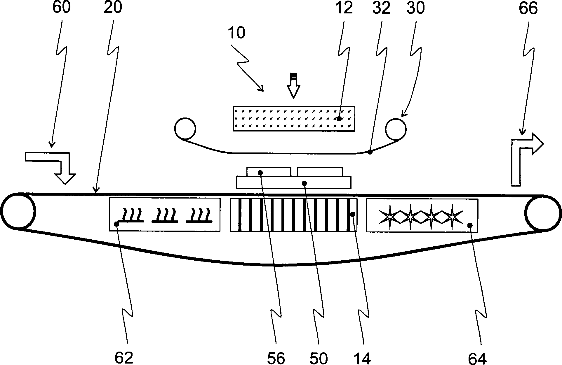
Die
erfinderische Lösung
wird an Hand der Ausführungsbeispiele
der
Weiterhin
dargestellt ist die Vorrichtung (
Weiterhin
dargestellt sind vorteilhafte Stationen der Vorrichtung. Zur Beladung
des Transportbands dient eine Beladestation (
Auf
diesen Leiterbahnen sind die chipförmigen Bauelemente (
Zwischen
der metallischen Kaschierung (
Weiterhin
ist ein Abschnitt des Transportbands (
Oberhalb
des Substrats (
Der
Pressstempel (
Hierbei
erfolgt die Druckeinleitung quasihydrostatische, da das Druckkissen
(
Claims (7)
Priority Applications (5)
| Application Number | Priority Date | Filing Date | Title |
|---|---|---|---|
| DE102005058794A DE102005058794A1 (en) | 2005-12-09 | 2005-12-09 | Device and clocked process for pressure sintering |
| DK06023023T DK1796137T3 (en) | 2005-12-09 | 2006-11-06 | A device and method for pulsed pressure inter-connection |
| ES06023023.2T ES2534205T3 (en) | 2005-12-09 | 2006-11-06 | Timed pressure sintering device and procedure |
| EP06023023.2A EP1796137B1 (en) | 2005-12-09 | 2006-11-06 | Apparatus and clocked method for pressure sintering |
| US11/636,845 US20070131353A1 (en) | 2005-12-09 | 2006-12-11 | Apparatus and clocked method for pressure-sintered bonding |
Applications Claiming Priority (1)
| Application Number | Priority Date | Filing Date | Title |
|---|---|---|---|
| DE102005058794A DE102005058794A1 (en) | 2005-12-09 | 2005-12-09 | Device and clocked process for pressure sintering |
Publications (1)
| Publication Number | Publication Date |
|---|---|
| DE102005058794A1 true DE102005058794A1 (en) | 2007-06-14 |
Family
ID=37896075
Family Applications (1)
| Application Number | Title | Priority Date | Filing Date |
|---|---|---|---|
| DE102005058794A Withdrawn DE102005058794A1 (en) | 2005-12-09 | 2005-12-09 | Device and clocked process for pressure sintering |
Country Status (5)
| Country | Link |
|---|---|
| US (1) | US20070131353A1 (en) |
| EP (1) | EP1796137B1 (en) |
| DE (1) | DE102005058794A1 (en) |
| DK (1) | DK1796137T3 (en) |
| ES (1) | ES2534205T3 (en) |
Cited By (14)
| Publication number | Priority date | Publication date | Assignee | Title |
|---|---|---|---|---|
| WO2009019091A1 (en) * | 2007-08-09 | 2009-02-12 | Robert Bosch Gmbh | Unit and production of a unit |
| EP2148556A2 (en) | 2008-07-26 | 2010-01-27 | Semikron Elektronik GmbH & Co. KG Patentabteilung | Noble metal connection and application method thereof |
| EP2148363A2 (en) | 2008-07-26 | 2010-01-27 | Semikron Elektronik GmbH & Co. KG Patentabteilung | Nobel metal based connection means with a solid fraction and a fluid fraction and application method for same |
| EP2147739A2 (en) | 2008-07-26 | 2010-01-27 | Semikron Elektronik GmbH & Co. KG Patentabteilung | Nobel metal based connection means in the form of a foil with a solid faction and a liquid fraction and application and production method for same |
| DE102010020696A1 (en) | 2010-05-17 | 2011-11-17 | Danfoss Silicon Power Gmbh | Method for sintering three-dimensional contour exhibiting semiconductor component for power electronics using low-temperature joining technique, involves applying sintering pressure by upper die with contours of semiconductor component |
| EP2390914A1 (en) | 2010-05-27 | 2011-11-30 | SEMIKRON Elektronik GmbH & Co. KG | Assembly of two connection partners with low temperature pressure interconnection and method for producing same |
| EP2390904A2 (en) | 2010-05-27 | 2011-11-30 | SEMIKRON Elektronik GmbH & Co. KG | Method for low temperature pressure interconnection of two connection partners and assembly manufactured using same |
| DE102007022338B4 (en) * | 2007-07-26 | 2013-12-05 | Semikron Elektronik Gmbh & Co. Kg | Manufacturing method for a power semiconductor device with metal contact layer |
| DE102012222791A1 (en) | 2012-12-11 | 2014-06-12 | Robert Bosch Gmbh | Method for contacting a semiconductor and semiconductor device with increased stability to thermomechanical influences |
| DE102013101124A1 (en) | 2013-02-05 | 2014-08-07 | Seho Systemtechnik Gmbh | Apparatus, useful for sintering product, comprises construction element and substrate having pressing unit that comprises table and stamp, where press stamp comprises pressure body coupled to heating device such that pressure body expands |
| DE102014103013A1 (en) * | 2014-03-06 | 2015-09-10 | Infineon Technologies Ag | Method for producing a dried paste layer, method for producing a sintered connection, method for producing a power semiconductor module and continuous-flow system |
| DE102014114095A1 (en) * | 2014-09-29 | 2016-03-31 | Danfoss Silicon Power Gmbh | sintering apparatus |
| DE102015120156A1 (en) | 2015-11-20 | 2017-05-24 | Semikron Elektronik Gmbh & Co. Kg | Device for material connection of connection partners of a Leistungselekronik component |
| DE102019105465B3 (en) * | 2019-03-04 | 2020-07-23 | Danfoss Silicon Power Gmbh | Pressure sintering device and method for producing an electronic component |
Families Citing this family (11)
| Publication number | Priority date | Publication date | Assignee | Title |
|---|---|---|---|---|
| US8293586B2 (en) | 2008-09-25 | 2012-10-23 | Infineon Technologies Ag | Method of manufacturing an electronic system |
| SE537052C2 (en) * | 2012-08-28 | 2014-12-16 | Copolia Company Sa | Device and method for dewatering wood chips |
| DE102014114096A1 (en) | 2014-09-29 | 2016-03-31 | Danfoss Silicon Power Gmbh | Sintering tool for the lower punch of a sintering device |
| DE102014114097B4 (en) | 2014-09-29 | 2017-06-01 | Danfoss Silicon Power Gmbh | Sintering tool and method for sintering an electronic assembly |
| DE102014114093B4 (en) * | 2014-09-29 | 2017-03-23 | Danfoss Silicon Power Gmbh | Method for low-temperature pressure sintering |
| DE102015107712B3 (en) * | 2015-05-18 | 2016-10-20 | Danfoss Silicon Power Gmbh | Method for producing a circuit carrier |
| NL2015895B1 (en) * | 2015-12-02 | 2017-06-28 | Besi Netherlands Bv | Device and method for thermal compression bonding electronic components on a carrier. |
| DE102017116372B3 (en) * | 2017-07-20 | 2018-10-18 | Semikron Elektronik Gmbh & Co. Kg | Pressure sintering method and pressure transmission device therefor |
| DE102019204683A1 (en) * | 2019-04-02 | 2020-10-08 | Volkswagen Aktiengesellschaft | Method and device for the material connection of at least one semiconductor module to at least one housing part of a cooling module |
| DE102019206896A1 (en) * | 2019-05-13 | 2020-11-19 | Siemens Aktiengesellschaft | Improvements in power semiconductor components on heat pipes |
| US11676937B2 (en) | 2021-05-04 | 2023-06-13 | Asmpt Singapore Pte. Ltd. | Flexible sinter tool for bonding semiconductor devices |
Citations (6)
| Publication number | Priority date | Publication date | Assignee | Title |
|---|---|---|---|---|
| DE3414065C2 (en) * | 1984-04-13 | 1989-07-27 | Siemens Ag, 1000 Berlin Und 8000 Muenchen, De | |
| EP0242626B1 (en) * | 1986-04-22 | 1991-06-12 | Siemens Aktiengesellschaft | Method for mounting electronic components on a substrate |
| EP1282162A2 (en) * | 2001-08-03 | 2003-02-05 | Matsushita Electric Industrial Co., Ltd. | Method for fabricating semiconductor-mounting body and apparatus for fabricating semiconductor-mounting body |
| US6544377B1 (en) * | 1997-11-20 | 2003-04-08 | Matsushita Electric Industrial Co., Ltd. | Heating and pressurizing apparatus for use in mounting electronic components, and apparatus and method for mounting electronic components |
| DE10245398B3 (en) * | 2002-09-28 | 2004-06-03 | Mühlbauer Ag | Device and method for applying semiconductor chips to carriers |
| DE102004019567B3 (en) * | 2004-04-22 | 2006-01-12 | Semikron Elektronik Gmbh & Co. Kg | Securing electronic components to substrate by subjecting the electronic component, supporting film and paste-like layer to pressure and connecting the substrate and the component by sintering |
Family Cites Families (6)
| Publication number | Priority date | Publication date | Assignee | Title |
|---|---|---|---|---|
| EP0330895B1 (en) * | 1988-03-03 | 1994-12-14 | Siemens Aktiengesellschaft | Method for attaching electronic components to substrates, and arrangement for carrying it out |
| EP0330896A3 (en) * | 1988-03-03 | 1991-01-09 | Siemens Aktiengesellschaft | Method for attaching semiconductor components to substrates, and arrangement for carrying it out |
| DK168368B1 (en) * | 1988-06-30 | 1994-03-21 | Milliken Denmark | Label for labeling a vulcanizable rubber blanket |
| US6152353A (en) * | 1999-01-14 | 2000-11-28 | Celestica International Inc. | Printed circuit board header attachment station |
| JP3949072B2 (en) | 2003-03-26 | 2007-07-25 | 日機装株式会社 | Pressurizing device |
| DE102004056702B3 (en) * | 2004-04-22 | 2006-03-02 | Semikron Elektronik Gmbh & Co. Kg | Method for mounting electronic components on a substrate |
-
2005
- 2005-12-09 DE DE102005058794A patent/DE102005058794A1/en not_active Withdrawn
-
2006
- 2006-11-06 DK DK06023023T patent/DK1796137T3/en active
- 2006-11-06 ES ES06023023.2T patent/ES2534205T3/en active Active
- 2006-11-06 EP EP06023023.2A patent/EP1796137B1/en active Active
- 2006-12-11 US US11/636,845 patent/US20070131353A1/en not_active Abandoned
Patent Citations (6)
| Publication number | Priority date | Publication date | Assignee | Title |
|---|---|---|---|---|
| DE3414065C2 (en) * | 1984-04-13 | 1989-07-27 | Siemens Ag, 1000 Berlin Und 8000 Muenchen, De | |
| EP0242626B1 (en) * | 1986-04-22 | 1991-06-12 | Siemens Aktiengesellschaft | Method for mounting electronic components on a substrate |
| US6544377B1 (en) * | 1997-11-20 | 2003-04-08 | Matsushita Electric Industrial Co., Ltd. | Heating and pressurizing apparatus for use in mounting electronic components, and apparatus and method for mounting electronic components |
| EP1282162A2 (en) * | 2001-08-03 | 2003-02-05 | Matsushita Electric Industrial Co., Ltd. | Method for fabricating semiconductor-mounting body and apparatus for fabricating semiconductor-mounting body |
| DE10245398B3 (en) * | 2002-09-28 | 2004-06-03 | Mühlbauer Ag | Device and method for applying semiconductor chips to carriers |
| DE102004019567B3 (en) * | 2004-04-22 | 2006-01-12 | Semikron Elektronik Gmbh & Co. Kg | Securing electronic components to substrate by subjecting the electronic component, supporting film and paste-like layer to pressure and connecting the substrate and the component by sintering |
Cited By (30)
| Publication number | Priority date | Publication date | Assignee | Title |
|---|---|---|---|---|
| DE102007022338B4 (en) * | 2007-07-26 | 2013-12-05 | Semikron Elektronik Gmbh & Co. Kg | Manufacturing method for a power semiconductor device with metal contact layer |
| US9233436B2 (en) | 2007-08-09 | 2016-01-12 | Robert Bosch Gmbh | Assembly and production of an assembly |
| US8552306B2 (en) | 2007-08-09 | 2013-10-08 | Robert Bosch Gmbh | Assembly and production of an assembly |
| WO2009019091A1 (en) * | 2007-08-09 | 2009-02-12 | Robert Bosch Gmbh | Unit and production of a unit |
| DE102008034952A1 (en) | 2008-07-26 | 2010-01-28 | Semikron Elektronik Gmbh & Co. Kg | Noble metal compounding agents and methods of use for this purpose |
| DE102008034946A1 (en) | 2008-07-26 | 2010-01-28 | Semikron Elektronik Gmbh & Co. Kg | Noble metal compounding agents as well as production and use methods for this purpose |
| DE102008034953A1 (en) | 2008-07-26 | 2010-01-28 | Semikron Elektronik Gmbh & Co. Kg | Noble metal compounding agents and methods of use for this purpose |
| EP2147739A2 (en) | 2008-07-26 | 2010-01-27 | Semikron Elektronik GmbH & Co. KG Patentabteilung | Nobel metal based connection means in the form of a foil with a solid faction and a liquid fraction and application and production method for same |
| EP2148363A2 (en) | 2008-07-26 | 2010-01-27 | Semikron Elektronik GmbH & Co. KG Patentabteilung | Nobel metal based connection means with a solid fraction and a fluid fraction and application method for same |
| EP2148556A2 (en) | 2008-07-26 | 2010-01-27 | Semikron Elektronik GmbH & Co. KG Patentabteilung | Noble metal connection and application method thereof |
| DE102010020696A1 (en) | 2010-05-17 | 2011-11-17 | Danfoss Silicon Power Gmbh | Method for sintering three-dimensional contour exhibiting semiconductor component for power electronics using low-temperature joining technique, involves applying sintering pressure by upper die with contours of semiconductor component |
| EP2390904A2 (en) | 2010-05-27 | 2011-11-30 | SEMIKRON Elektronik GmbH & Co. KG | Method for low temperature pressure interconnection of two connection partners and assembly manufactured using same |
| DE102010021764A1 (en) | 2010-05-27 | 2011-12-01 | Semikron Elektronik Gmbh & Co. Kg | Process for the low-temperature pressure sintering connection of two connection partners and arrangement produced thereby |
| CN102263068A (en) * | 2010-05-27 | 2011-11-30 | 赛米控电子股份有限公司 | Assembly of two connection partners with low temperature pressure interconnection and method for producing same |
| EP2390914A1 (en) | 2010-05-27 | 2011-11-30 | SEMIKRON Elektronik GmbH & Co. KG | Assembly of two connection partners with low temperature pressure interconnection and method for producing same |
| DE102010021765B4 (en) * | 2010-05-27 | 2014-06-12 | Semikron Elektronik Gmbh & Co. Kg | Manufacturing method for the arrangement of two connection partners by means of a low-temperature pressure sintered connection |
| DE102010021765A1 (en) | 2010-05-27 | 2011-12-01 | Semikron Elektronik Gmbh & Co. Kg | Arrangement of two connection partners with a low-temperature pressure sintered interconnect production method |
| CN102263068B (en) * | 2010-05-27 | 2015-08-26 | 赛米控电子股份有限公司 | Two the connection mating member systems connected with low-temperature pressure sintering and manufacture method thereof |
| EP2743973A2 (en) | 2012-12-11 | 2014-06-18 | Robert Bosch Gmbh | Method for contacting a semiconductor element by welding a contact element to a sintered layer on the semiconductor element and semiconductor component with increased stability against thermomechanical influence |
| DE102012222791A1 (en) | 2012-12-11 | 2014-06-12 | Robert Bosch Gmbh | Method for contacting a semiconductor and semiconductor device with increased stability to thermomechanical influences |
| DE102013101124B4 (en) * | 2013-02-05 | 2020-12-03 | Seho Systemtechnik Gmbh | Device and method for sintering a sintered product |
| DE102013101124A1 (en) | 2013-02-05 | 2014-08-07 | Seho Systemtechnik Gmbh | Apparatus, useful for sintering product, comprises construction element and substrate having pressing unit that comprises table and stamp, where press stamp comprises pressure body coupled to heating device such that pressure body expands |
| DE102014103013A1 (en) * | 2014-03-06 | 2015-09-10 | Infineon Technologies Ag | Method for producing a dried paste layer, method for producing a sintered connection, method for producing a power semiconductor module and continuous-flow system |
| DE102014103013B4 (en) * | 2014-03-06 | 2017-09-21 | Infineon Technologies Ag | Method for producing a dried paste layer, method for producing a sintered connection and continuous system for carrying out the method |
| DE102014114095B4 (en) * | 2014-09-29 | 2017-03-23 | Danfoss Silicon Power Gmbh | sintering apparatus |
| DE102014114095A1 (en) * | 2014-09-29 | 2016-03-31 | Danfoss Silicon Power Gmbh | sintering apparatus |
| DE102015120156A1 (en) | 2015-11-20 | 2017-05-24 | Semikron Elektronik Gmbh & Co. Kg | Device for material connection of connection partners of a Leistungselekronik component |
| DE102015120156B4 (en) | 2015-11-20 | 2019-07-04 | Semikron Elektronik Gmbh & Co. Kg | Device for the material connection of connection partners of a Leistungselekronik component and use of such a device |
| US10603741B2 (en) | 2015-11-20 | 2020-03-31 | Semikron Elektronik Gmbh & Co., Kg | Apparatus for the material-bonded connection of connection partners of a power-electronics component |
| DE102019105465B3 (en) * | 2019-03-04 | 2020-07-23 | Danfoss Silicon Power Gmbh | Pressure sintering device and method for producing an electronic component |
Also Published As
| Publication number | Publication date |
|---|---|
| EP1796137B1 (en) | 2015-01-07 |
| EP1796137A2 (en) | 2007-06-13 |
| DK1796137T3 (en) | 2015-04-13 |
| ES2534205T3 (en) | 2015-04-20 |
| EP1796137A3 (en) | 2011-05-04 |
| US20070131353A1 (en) | 2007-06-14 |
Similar Documents
| Publication | Publication Date | Title |
|---|---|---|
| EP1796137B1 (en) | Apparatus and clocked method for pressure sintering | |
| DE102015120156B4 (en) | Device for the material connection of connection partners of a Leistungselekronik component and use of such a device | |
| DE102013216633B4 (en) | Pre-sintered semiconductor chip structure and method of manufacture | |
| DE102014103013B4 (en) | Method for producing a dried paste layer, method for producing a sintered connection and continuous system for carrying out the method | |
| DE102004019567B3 (en) | Securing electronic components to substrate by subjecting the electronic component, supporting film and paste-like layer to pressure and connecting the substrate and the component by sintering | |
| DE102010021764B4 (en) | Method for low-temperature pressure sintering of two connection partners | |
| DE102016208196B4 (en) | Method for the generative production of three-dimensional composite components | |
| WO2007137547A1 (en) | Method and device for heat treatment, especially connection by soldering | |
| EP2205391B1 (en) | Method for operation of a wave soldering system which uses perfluoric polyether for reaction with impurities containing lead | |
| DE102015225757A1 (en) | Device and method for the continuous generative production of components | |
| EP3123500A1 (en) | Carrier and clip each having sinterable, solidified paste for connection to a semiconductor element, corresponding sintering paste, and corresponding production method and use | |
| DE2359154C2 (en) | Soldering arrangement | |
| DE2357625A1 (en) | PROCESS AND DEVICE FOR MANUFACTURING CERAMIC-METAL COMPONENTS | |
| WO2010083976A1 (en) | Device for soldering a conductor onto a circuit carrier | |
| EP2498283B1 (en) | Method for manufacturing a power-semiconductor substrate | |
| DE2358279C3 (en) | Reaction vessel for depositing semiconductor material on heated substrates | |
| EP3639950A1 (en) | Device for producing metallic or ceramic parts | |
| DE102007022338B4 (en) | Manufacturing method for a power semiconductor device with metal contact layer | |
| DE102014114096A1 (en) | Sintering tool for the lower punch of a sintering device | |
| WO2019115557A1 (en) | Method and device for equipping an antenna structure with an electronic component | |
| DE102022102745A1 (en) | Apparatus and method for pressurized sintering | |
| EP1514302B1 (en) | Device for producing an electronic component having external contact surfaces and use of the device for producing an electronic component | |
| DE2722140C2 (en) | Method and device for metallizing the end faces of ceramic multilayer capacitors or other electrical components | |
| EP3785829A1 (en) | Substrate semifinished product comprising a sintered material | |
| EP3275576A1 (en) | Method for connection of metallic building components |
Legal Events
| Date | Code | Title | Description |
|---|---|---|---|
| OP8 | Request for examination as to paragraph 44 patent law | ||
| R130 | Divisional application to |
Ref document number: 102005063643 Country of ref document: DE |
|
| R119 | Application deemed withdrawn, or ip right lapsed, due to non-payment of renewal fee |