EP2390904A2 - Method for low temperature pressure interconnection of two connection partners and assembly manufactured using same - Google Patents
Method for low temperature pressure interconnection of two connection partners and assembly manufactured using same Download PDFInfo
- Publication number
- EP2390904A2 EP2390904A2 EP11162103A EP11162103A EP2390904A2 EP 2390904 A2 EP2390904 A2 EP 2390904A2 EP 11162103 A EP11162103 A EP 11162103A EP 11162103 A EP11162103 A EP 11162103A EP 2390904 A2 EP2390904 A2 EP 2390904A2
- Authority
- EP
- European Patent Office
- Prior art keywords
- connection
- layer
- sintered
- contact surface
- partners
- Prior art date
- Legal status (The legal status is an assumption and is not a legal conclusion. Google has not performed a legal analysis and makes no representation as to the accuracy of the status listed.)
- Withdrawn
Links
Images

Classifications
-
- H—ELECTRICITY
- H01—ELECTRIC ELEMENTS
- H01L—SEMICONDUCTOR DEVICES NOT COVERED BY CLASS H10
- H01L24/00—Arrangements for connecting or disconnecting semiconductor or solid-state bodies; Methods or apparatus related thereto
- H01L24/80—Methods for connecting semiconductor or other solid state bodies using means for bonding being attached to, or being formed on, the surface to be connected
- H01L24/83—Methods for connecting semiconductor or other solid state bodies using means for bonding being attached to, or being formed on, the surface to be connected using a layer connector
-
- H—ELECTRICITY
- H01—ELECTRIC ELEMENTS
- H01L—SEMICONDUCTOR DEVICES NOT COVERED BY CLASS H10
- H01L24/00—Arrangements for connecting or disconnecting semiconductor or solid-state bodies; Methods or apparatus related thereto
- H01L24/01—Means for bonding being attached to, or being formed on, the surface to be connected, e.g. chip-to-package, die-attach, "first-level" interconnects; Manufacturing methods related thereto
- H01L24/26—Layer connectors, e.g. plate connectors, solder or adhesive layers; Manufacturing methods related thereto
- H01L24/27—Manufacturing methods
-
- H—ELECTRICITY
- H01—ELECTRIC ELEMENTS
- H01L—SEMICONDUCTOR DEVICES NOT COVERED BY CLASS H10
- H01L24/00—Arrangements for connecting or disconnecting semiconductor or solid-state bodies; Methods or apparatus related thereto
- H01L24/01—Means for bonding being attached to, or being formed on, the surface to be connected, e.g. chip-to-package, die-attach, "first-level" interconnects; Manufacturing methods related thereto
- H01L24/26—Layer connectors, e.g. plate connectors, solder or adhesive layers; Manufacturing methods related thereto
- H01L24/28—Structure, shape, material or disposition of the layer connectors prior to the connecting process
- H01L24/29—Structure, shape, material or disposition of the layer connectors prior to the connecting process of an individual layer connector
-
- H—ELECTRICITY
- H01—ELECTRIC ELEMENTS
- H01L—SEMICONDUCTOR DEVICES NOT COVERED BY CLASS H10
- H01L2224/00—Indexing scheme for arrangements for connecting or disconnecting semiconductor or solid-state bodies and methods related thereto as covered by H01L24/00
- H01L2224/01—Means for bonding being attached to, or being formed on, the surface to be connected, e.g. chip-to-package, die-attach, "first-level" interconnects; Manufacturing methods related thereto
- H01L2224/02—Bonding areas; Manufacturing methods related thereto
- H01L2224/04—Structure, shape, material or disposition of the bonding areas prior to the connecting process
- H01L2224/06—Structure, shape, material or disposition of the bonding areas prior to the connecting process of a plurality of bonding areas
- H01L2224/0601—Structure
- H01L2224/0603—Bonding areas having different sizes, e.g. different heights or widths
-
- H—ELECTRICITY
- H01—ELECTRIC ELEMENTS
- H01L—SEMICONDUCTOR DEVICES NOT COVERED BY CLASS H10
- H01L2224/00—Indexing scheme for arrangements for connecting or disconnecting semiconductor or solid-state bodies and methods related thereto as covered by H01L24/00
- H01L2224/01—Means for bonding being attached to, or being formed on, the surface to be connected, e.g. chip-to-package, die-attach, "first-level" interconnects; Manufacturing methods related thereto
- H01L2224/02—Bonding areas; Manufacturing methods related thereto
- H01L2224/04—Structure, shape, material or disposition of the bonding areas prior to the connecting process
- H01L2224/06—Structure, shape, material or disposition of the bonding areas prior to the connecting process of a plurality of bonding areas
- H01L2224/061—Disposition
- H01L2224/0618—Disposition being disposed on at least two different sides of the body, e.g. dual array
- H01L2224/06181—On opposite sides of the body
-
- H—ELECTRICITY
- H01—ELECTRIC ELEMENTS
- H01L—SEMICONDUCTOR DEVICES NOT COVERED BY CLASS H10
- H01L2224/00—Indexing scheme for arrangements for connecting or disconnecting semiconductor or solid-state bodies and methods related thereto as covered by H01L24/00
- H01L2224/01—Means for bonding being attached to, or being formed on, the surface to be connected, e.g. chip-to-package, die-attach, "first-level" interconnects; Manufacturing methods related thereto
- H01L2224/26—Layer connectors, e.g. plate connectors, solder or adhesive layers; Manufacturing methods related thereto
- H01L2224/27—Manufacturing methods
- H01L2224/273—Manufacturing methods by local deposition of the material of the layer connector
- H01L2224/2731—Manufacturing methods by local deposition of the material of the layer connector in liquid form
- H01L2224/2732—Screen printing, i.e. using a stencil
-
- H—ELECTRICITY
- H01—ELECTRIC ELEMENTS
- H01L—SEMICONDUCTOR DEVICES NOT COVERED BY CLASS H10
- H01L2224/00—Indexing scheme for arrangements for connecting or disconnecting semiconductor or solid-state bodies and methods related thereto as covered by H01L24/00
- H01L2224/01—Means for bonding being attached to, or being formed on, the surface to be connected, e.g. chip-to-package, die-attach, "first-level" interconnects; Manufacturing methods related thereto
- H01L2224/26—Layer connectors, e.g. plate connectors, solder or adhesive layers; Manufacturing methods related thereto
- H01L2224/27—Manufacturing methods
- H01L2224/278—Post-treatment of the layer connector
- H01L2224/27848—Thermal treatments, e.g. annealing, controlled cooling
-
- H—ELECTRICITY
- H01—ELECTRIC ELEMENTS
- H01L—SEMICONDUCTOR DEVICES NOT COVERED BY CLASS H10
- H01L2224/00—Indexing scheme for arrangements for connecting or disconnecting semiconductor or solid-state bodies and methods related thereto as covered by H01L24/00
- H01L2224/01—Means for bonding being attached to, or being formed on, the surface to be connected, e.g. chip-to-package, die-attach, "first-level" interconnects; Manufacturing methods related thereto
- H01L2224/26—Layer connectors, e.g. plate connectors, solder or adhesive layers; Manufacturing methods related thereto
- H01L2224/28—Structure, shape, material or disposition of the layer connectors prior to the connecting process
- H01L2224/29—Structure, shape, material or disposition of the layer connectors prior to the connecting process of an individual layer connector
- H01L2224/29001—Core members of the layer connector
- H01L2224/29075—Plural core members
- H01L2224/2908—Plural core members being stacked
- H01L2224/29082—Two-layer arrangements
-
- H—ELECTRICITY
- H01—ELECTRIC ELEMENTS
- H01L—SEMICONDUCTOR DEVICES NOT COVERED BY CLASS H10
- H01L2224/00—Indexing scheme for arrangements for connecting or disconnecting semiconductor or solid-state bodies and methods related thereto as covered by H01L24/00
- H01L2224/01—Means for bonding being attached to, or being formed on, the surface to be connected, e.g. chip-to-package, die-attach, "first-level" interconnects; Manufacturing methods related thereto
- H01L2224/26—Layer connectors, e.g. plate connectors, solder or adhesive layers; Manufacturing methods related thereto
- H01L2224/28—Structure, shape, material or disposition of the layer connectors prior to the connecting process
- H01L2224/29—Structure, shape, material or disposition of the layer connectors prior to the connecting process of an individual layer connector
- H01L2224/29001—Core members of the layer connector
- H01L2224/29099—Material
- H01L2224/2919—Material with a principal constituent of the material being a polymer, e.g. polyester, phenolic based polymer, epoxy
- H01L2224/29191—The principal constituent being an elastomer, e.g. silicones, isoprene, neoprene
-
- H—ELECTRICITY
- H01—ELECTRIC ELEMENTS
- H01L—SEMICONDUCTOR DEVICES NOT COVERED BY CLASS H10
- H01L2224/00—Indexing scheme for arrangements for connecting or disconnecting semiconductor or solid-state bodies and methods related thereto as covered by H01L24/00
- H01L2224/01—Means for bonding being attached to, or being formed on, the surface to be connected, e.g. chip-to-package, die-attach, "first-level" interconnects; Manufacturing methods related thereto
- H01L2224/26—Layer connectors, e.g. plate connectors, solder or adhesive layers; Manufacturing methods related thereto
- H01L2224/28—Structure, shape, material or disposition of the layer connectors prior to the connecting process
- H01L2224/29—Structure, shape, material or disposition of the layer connectors prior to the connecting process of an individual layer connector
- H01L2224/29001—Core members of the layer connector
- H01L2224/29099—Material
- H01L2224/29198—Material with a principal constituent of the material being a combination of two or more materials in the form of a matrix with a filler, i.e. being a hybrid material, e.g. segmented structures, foams
- H01L2224/29199—Material of the matrix
- H01L2224/292—Material of the matrix with a principal constituent of the material being a metal or a metalloid, e.g. boron [B], silicon [Si], germanium [Ge], arsenic [As], antimony [Sb], tellurium [Te] and polonium [Po], and alloys thereof
- H01L2224/29238—Material of the matrix with a principal constituent of the material being a metal or a metalloid, e.g. boron [B], silicon [Si], germanium [Ge], arsenic [As], antimony [Sb], tellurium [Te] and polonium [Po], and alloys thereof the principal constituent melting at a temperature of greater than or equal to 950°C and less than 1550°C
- H01L2224/29239—Silver [Ag] as principal constituent
-
- H—ELECTRICITY
- H01—ELECTRIC ELEMENTS
- H01L—SEMICONDUCTOR DEVICES NOT COVERED BY CLASS H10
- H01L2224/00—Indexing scheme for arrangements for connecting or disconnecting semiconductor or solid-state bodies and methods related thereto as covered by H01L24/00
- H01L2224/01—Means for bonding being attached to, or being formed on, the surface to be connected, e.g. chip-to-package, die-attach, "first-level" interconnects; Manufacturing methods related thereto
- H01L2224/26—Layer connectors, e.g. plate connectors, solder or adhesive layers; Manufacturing methods related thereto
- H01L2224/28—Structure, shape, material or disposition of the layer connectors prior to the connecting process
- H01L2224/29—Structure, shape, material or disposition of the layer connectors prior to the connecting process of an individual layer connector
- H01L2224/29001—Core members of the layer connector
- H01L2224/29099—Material
- H01L2224/29198—Material with a principal constituent of the material being a combination of two or more materials in the form of a matrix with a filler, i.e. being a hybrid material, e.g. segmented structures, foams
- H01L2224/29199—Material of the matrix
- H01L2224/29294—Material of the matrix with a principal constituent of the material being a liquid not provided for in groups H01L2224/292 - H01L2224/29291
-
- H—ELECTRICITY
- H01—ELECTRIC ELEMENTS
- H01L—SEMICONDUCTOR DEVICES NOT COVERED BY CLASS H10
- H01L2224/00—Indexing scheme for arrangements for connecting or disconnecting semiconductor or solid-state bodies and methods related thereto as covered by H01L24/00
- H01L2224/01—Means for bonding being attached to, or being formed on, the surface to be connected, e.g. chip-to-package, die-attach, "first-level" interconnects; Manufacturing methods related thereto
- H01L2224/26—Layer connectors, e.g. plate connectors, solder or adhesive layers; Manufacturing methods related thereto
- H01L2224/28—Structure, shape, material or disposition of the layer connectors prior to the connecting process
- H01L2224/29—Structure, shape, material or disposition of the layer connectors prior to the connecting process of an individual layer connector
- H01L2224/29001—Core members of the layer connector
- H01L2224/29099—Material
- H01L2224/29198—Material with a principal constituent of the material being a combination of two or more materials in the form of a matrix with a filler, i.e. being a hybrid material, e.g. segmented structures, foams
- H01L2224/29298—Fillers
- H01L2224/29299—Base material
- H01L2224/293—Base material with a principal constituent of the material being a metal or a metalloid, e.g. boron [B], silicon [Si], germanium [Ge], arsenic [As], antimony [Sb], tellurium [Te] and polonium [Po], and alloys thereof
- H01L2224/29338—Base material with a principal constituent of the material being a metal or a metalloid, e.g. boron [B], silicon [Si], germanium [Ge], arsenic [As], antimony [Sb], tellurium [Te] and polonium [Po], and alloys thereof the principal constituent melting at a temperature of greater than or equal to 950°C and less than 1550°C
- H01L2224/29339—Silver [Ag] as principal constituent
-
- H—ELECTRICITY
- H01—ELECTRIC ELEMENTS
- H01L—SEMICONDUCTOR DEVICES NOT COVERED BY CLASS H10
- H01L2224/00—Indexing scheme for arrangements for connecting or disconnecting semiconductor or solid-state bodies and methods related thereto as covered by H01L24/00
- H01L2224/01—Means for bonding being attached to, or being formed on, the surface to be connected, e.g. chip-to-package, die-attach, "first-level" interconnects; Manufacturing methods related thereto
- H01L2224/26—Layer connectors, e.g. plate connectors, solder or adhesive layers; Manufacturing methods related thereto
- H01L2224/28—Structure, shape, material or disposition of the layer connectors prior to the connecting process
- H01L2224/29—Structure, shape, material or disposition of the layer connectors prior to the connecting process of an individual layer connector
- H01L2224/29001—Core members of the layer connector
- H01L2224/29099—Material
- H01L2224/29198—Material with a principal constituent of the material being a combination of two or more materials in the form of a matrix with a filler, i.e. being a hybrid material, e.g. segmented structures, foams
- H01L2224/29298—Fillers
- H01L2224/29299—Base material
- H01L2224/29395—Base material with a principal constituent of the material being a gas not provided for in groups H01L2224/293 - H01L2224/29391
-
- H—ELECTRICITY
- H01—ELECTRIC ELEMENTS
- H01L—SEMICONDUCTOR DEVICES NOT COVERED BY CLASS H10
- H01L2224/00—Indexing scheme for arrangements for connecting or disconnecting semiconductor or solid-state bodies and methods related thereto as covered by H01L24/00
- H01L2224/01—Means for bonding being attached to, or being formed on, the surface to be connected, e.g. chip-to-package, die-attach, "first-level" interconnects; Manufacturing methods related thereto
- H01L2224/26—Layer connectors, e.g. plate connectors, solder or adhesive layers; Manufacturing methods related thereto
- H01L2224/31—Structure, shape, material or disposition of the layer connectors after the connecting process
- H01L2224/32—Structure, shape, material or disposition of the layer connectors after the connecting process of an individual layer connector
- H01L2224/3201—Structure
- H01L2224/32012—Structure relative to the bonding area, e.g. bond pad
- H01L2224/32014—Structure relative to the bonding area, e.g. bond pad the layer connector being smaller than the bonding area, e.g. bond pad
-
- H—ELECTRICITY
- H01—ELECTRIC ELEMENTS
- H01L—SEMICONDUCTOR DEVICES NOT COVERED BY CLASS H10
- H01L2224/00—Indexing scheme for arrangements for connecting or disconnecting semiconductor or solid-state bodies and methods related thereto as covered by H01L24/00
- H01L2224/01—Means for bonding being attached to, or being formed on, the surface to be connected, e.g. chip-to-package, die-attach, "first-level" interconnects; Manufacturing methods related thereto
- H01L2224/26—Layer connectors, e.g. plate connectors, solder or adhesive layers; Manufacturing methods related thereto
- H01L2224/31—Structure, shape, material or disposition of the layer connectors after the connecting process
- H01L2224/32—Structure, shape, material or disposition of the layer connectors after the connecting process of an individual layer connector
- H01L2224/3205—Shape
- H01L2224/32052—Shape in top view
-
- H—ELECTRICITY
- H01—ELECTRIC ELEMENTS
- H01L—SEMICONDUCTOR DEVICES NOT COVERED BY CLASS H10
- H01L2224/00—Indexing scheme for arrangements for connecting or disconnecting semiconductor or solid-state bodies and methods related thereto as covered by H01L24/00
- H01L2224/01—Means for bonding being attached to, or being formed on, the surface to be connected, e.g. chip-to-package, die-attach, "first-level" interconnects; Manufacturing methods related thereto
- H01L2224/26—Layer connectors, e.g. plate connectors, solder or adhesive layers; Manufacturing methods related thereto
- H01L2224/31—Structure, shape, material or disposition of the layer connectors after the connecting process
- H01L2224/32—Structure, shape, material or disposition of the layer connectors after the connecting process of an individual layer connector
- H01L2224/3205—Shape
- H01L2224/32057—Shape in side view
- H01L2224/32058—Shape in side view being non uniform along the layer connector
-
- H—ELECTRICITY
- H01—ELECTRIC ELEMENTS
- H01L—SEMICONDUCTOR DEVICES NOT COVERED BY CLASS H10
- H01L2224/00—Indexing scheme for arrangements for connecting or disconnecting semiconductor or solid-state bodies and methods related thereto as covered by H01L24/00
- H01L2224/01—Means for bonding being attached to, or being formed on, the surface to be connected, e.g. chip-to-package, die-attach, "first-level" interconnects; Manufacturing methods related thereto
- H01L2224/26—Layer connectors, e.g. plate connectors, solder or adhesive layers; Manufacturing methods related thereto
- H01L2224/31—Structure, shape, material or disposition of the layer connectors after the connecting process
- H01L2224/32—Structure, shape, material or disposition of the layer connectors after the connecting process of an individual layer connector
- H01L2224/321—Disposition
- H01L2224/32151—Disposition the layer connector connecting between a semiconductor or solid-state body and an item not being a semiconductor or solid-state body, e.g. chip-to-substrate, chip-to-passive
- H01L2224/32221—Disposition the layer connector connecting between a semiconductor or solid-state body and an item not being a semiconductor or solid-state body, e.g. chip-to-substrate, chip-to-passive the body and the item being stacked
- H01L2224/32225—Disposition the layer connector connecting between a semiconductor or solid-state body and an item not being a semiconductor or solid-state body, e.g. chip-to-substrate, chip-to-passive the body and the item being stacked the item being non-metallic, e.g. insulating substrate with or without metallisation
- H01L2224/32227—Disposition the layer connector connecting between a semiconductor or solid-state body and an item not being a semiconductor or solid-state body, e.g. chip-to-substrate, chip-to-passive the body and the item being stacked the item being non-metallic, e.g. insulating substrate with or without metallisation the layer connector connecting to a bond pad of the item
-
- H—ELECTRICITY
- H01—ELECTRIC ELEMENTS
- H01L—SEMICONDUCTOR DEVICES NOT COVERED BY CLASS H10
- H01L2224/00—Indexing scheme for arrangements for connecting or disconnecting semiconductor or solid-state bodies and methods related thereto as covered by H01L24/00
- H01L2224/01—Means for bonding being attached to, or being formed on, the surface to be connected, e.g. chip-to-package, die-attach, "first-level" interconnects; Manufacturing methods related thereto
- H01L2224/26—Layer connectors, e.g. plate connectors, solder or adhesive layers; Manufacturing methods related thereto
- H01L2224/31—Structure, shape, material or disposition of the layer connectors after the connecting process
- H01L2224/32—Structure, shape, material or disposition of the layer connectors after the connecting process of an individual layer connector
- H01L2224/321—Disposition
- H01L2224/32151—Disposition the layer connector connecting between a semiconductor or solid-state body and an item not being a semiconductor or solid-state body, e.g. chip-to-substrate, chip-to-passive
- H01L2224/32221—Disposition the layer connector connecting between a semiconductor or solid-state body and an item not being a semiconductor or solid-state body, e.g. chip-to-substrate, chip-to-passive the body and the item being stacked
- H01L2224/32225—Disposition the layer connector connecting between a semiconductor or solid-state body and an item not being a semiconductor or solid-state body, e.g. chip-to-substrate, chip-to-passive the body and the item being stacked the item being non-metallic, e.g. insulating substrate with or without metallisation
- H01L2224/32238—Disposition the layer connector connecting between a semiconductor or solid-state body and an item not being a semiconductor or solid-state body, e.g. chip-to-substrate, chip-to-passive the body and the item being stacked the item being non-metallic, e.g. insulating substrate with or without metallisation the layer connector connecting to a bonding area protruding from the surface of the item
-
- H—ELECTRICITY
- H01—ELECTRIC ELEMENTS
- H01L—SEMICONDUCTOR DEVICES NOT COVERED BY CLASS H10
- H01L2224/00—Indexing scheme for arrangements for connecting or disconnecting semiconductor or solid-state bodies and methods related thereto as covered by H01L24/00
- H01L2224/01—Means for bonding being attached to, or being formed on, the surface to be connected, e.g. chip-to-package, die-attach, "first-level" interconnects; Manufacturing methods related thereto
- H01L2224/26—Layer connectors, e.g. plate connectors, solder or adhesive layers; Manufacturing methods related thereto
- H01L2224/31—Structure, shape, material or disposition of the layer connectors after the connecting process
- H01L2224/33—Structure, shape, material or disposition of the layer connectors after the connecting process of a plurality of layer connectors
- H01L2224/3301—Structure
- H01L2224/3303—Layer connectors having different sizes, e.g. different heights or widths
-
- H—ELECTRICITY
- H01—ELECTRIC ELEMENTS
- H01L—SEMICONDUCTOR DEVICES NOT COVERED BY CLASS H10
- H01L2224/00—Indexing scheme for arrangements for connecting or disconnecting semiconductor or solid-state bodies and methods related thereto as covered by H01L24/00
- H01L2224/01—Means for bonding being attached to, or being formed on, the surface to be connected, e.g. chip-to-package, die-attach, "first-level" interconnects; Manufacturing methods related thereto
- H01L2224/26—Layer connectors, e.g. plate connectors, solder or adhesive layers; Manufacturing methods related thereto
- H01L2224/31—Structure, shape, material or disposition of the layer connectors after the connecting process
- H01L2224/33—Structure, shape, material or disposition of the layer connectors after the connecting process of a plurality of layer connectors
- H01L2224/331—Disposition
- H01L2224/3318—Disposition being disposed on at least two different sides of the body, e.g. dual array
- H01L2224/33183—On contiguous sides of the body
-
- H—ELECTRICITY
- H01—ELECTRIC ELEMENTS
- H01L—SEMICONDUCTOR DEVICES NOT COVERED BY CLASS H10
- H01L2224/00—Indexing scheme for arrangements for connecting or disconnecting semiconductor or solid-state bodies and methods related thereto as covered by H01L24/00
- H01L2224/80—Methods for connecting semiconductor or other solid state bodies using means for bonding being attached to, or being formed on, the surface to be connected
- H01L2224/83—Methods for connecting semiconductor or other solid state bodies using means for bonding being attached to, or being formed on, the surface to be connected using a layer connector
- H01L2224/83001—Methods for connecting semiconductor or other solid state bodies using means for bonding being attached to, or being formed on, the surface to be connected using a layer connector involving a temporary auxiliary member not forming part of the bonding apparatus
- H01L2224/83002—Methods for connecting semiconductor or other solid state bodies using means for bonding being attached to, or being formed on, the surface to be connected using a layer connector involving a temporary auxiliary member not forming part of the bonding apparatus being a removable or sacrificial coating
-
- H—ELECTRICITY
- H01—ELECTRIC ELEMENTS
- H01L—SEMICONDUCTOR DEVICES NOT COVERED BY CLASS H10
- H01L2224/00—Indexing scheme for arrangements for connecting or disconnecting semiconductor or solid-state bodies and methods related thereto as covered by H01L24/00
- H01L2224/80—Methods for connecting semiconductor or other solid state bodies using means for bonding being attached to, or being formed on, the surface to be connected
- H01L2224/83—Methods for connecting semiconductor or other solid state bodies using means for bonding being attached to, or being formed on, the surface to be connected using a layer connector
- H01L2224/83009—Pre-treatment of the layer connector or the bonding area
- H01L2224/83022—Cleaning the bonding area, e.g. oxide removal step, desmearing
-
- H—ELECTRICITY
- H01—ELECTRIC ELEMENTS
- H01L—SEMICONDUCTOR DEVICES NOT COVERED BY CLASS H10
- H01L2224/00—Indexing scheme for arrangements for connecting or disconnecting semiconductor or solid-state bodies and methods related thereto as covered by H01L24/00
- H01L2224/80—Methods for connecting semiconductor or other solid state bodies using means for bonding being attached to, or being formed on, the surface to be connected
- H01L2224/83—Methods for connecting semiconductor or other solid state bodies using means for bonding being attached to, or being formed on, the surface to be connected using a layer connector
- H01L2224/831—Methods for connecting semiconductor or other solid state bodies using means for bonding being attached to, or being formed on, the surface to be connected using a layer connector the layer connector being supplied to the parts to be connected in the bonding apparatus
-
- H—ELECTRICITY
- H01—ELECTRIC ELEMENTS
- H01L—SEMICONDUCTOR DEVICES NOT COVERED BY CLASS H10
- H01L2224/00—Indexing scheme for arrangements for connecting or disconnecting semiconductor or solid-state bodies and methods related thereto as covered by H01L24/00
- H01L2224/80—Methods for connecting semiconductor or other solid state bodies using means for bonding being attached to, or being formed on, the surface to be connected
- H01L2224/83—Methods for connecting semiconductor or other solid state bodies using means for bonding being attached to, or being formed on, the surface to be connected using a layer connector
- H01L2224/8319—Arrangement of the layer connectors prior to mounting
- H01L2224/83192—Arrangement of the layer connectors prior to mounting wherein the layer connectors are disposed only on another item or body to be connected to the semiconductor or solid-state body
-
- H—ELECTRICITY
- H01—ELECTRIC ELEMENTS
- H01L—SEMICONDUCTOR DEVICES NOT COVERED BY CLASS H10
- H01L2224/00—Indexing scheme for arrangements for connecting or disconnecting semiconductor or solid-state bodies and methods related thereto as covered by H01L24/00
- H01L2224/80—Methods for connecting semiconductor or other solid state bodies using means for bonding being attached to, or being formed on, the surface to be connected
- H01L2224/83—Methods for connecting semiconductor or other solid state bodies using means for bonding being attached to, or being formed on, the surface to be connected using a layer connector
- H01L2224/832—Applying energy for connecting
- H01L2224/83201—Compression bonding
- H01L2224/83203—Thermocompression bonding, e.g. diffusion bonding, pressure joining, thermocompression welding or solid-state welding
-
- H—ELECTRICITY
- H01—ELECTRIC ELEMENTS
- H01L—SEMICONDUCTOR DEVICES NOT COVERED BY CLASS H10
- H01L2224/00—Indexing scheme for arrangements for connecting or disconnecting semiconductor or solid-state bodies and methods related thereto as covered by H01L24/00
- H01L2224/80—Methods for connecting semiconductor or other solid state bodies using means for bonding being attached to, or being formed on, the surface to be connected
- H01L2224/83—Methods for connecting semiconductor or other solid state bodies using means for bonding being attached to, or being formed on, the surface to be connected using a layer connector
- H01L2224/8338—Bonding interfaces outside the semiconductor or solid-state body
- H01L2224/83399—Material
- H01L2224/834—Material with a principal constituent of the material being a metal or a metalloid, e.g. boron [B], silicon [Si], germanium [Ge], arsenic [As], antimony [Sb], tellurium [Te] and polonium [Po], and alloys thereof
- H01L2224/83438—Material with a principal constituent of the material being a metal or a metalloid, e.g. boron [B], silicon [Si], germanium [Ge], arsenic [As], antimony [Sb], tellurium [Te] and polonium [Po], and alloys thereof the principal constituent melting at a temperature of greater than or equal to 950°C and less than 1550°C
-
- H—ELECTRICITY
- H01—ELECTRIC ELEMENTS
- H01L—SEMICONDUCTOR DEVICES NOT COVERED BY CLASS H10
- H01L2224/00—Indexing scheme for arrangements for connecting or disconnecting semiconductor or solid-state bodies and methods related thereto as covered by H01L24/00
- H01L2224/80—Methods for connecting semiconductor or other solid state bodies using means for bonding being attached to, or being formed on, the surface to be connected
- H01L2224/83—Methods for connecting semiconductor or other solid state bodies using means for bonding being attached to, or being formed on, the surface to be connected using a layer connector
- H01L2224/838—Bonding techniques
- H01L2224/8384—Sintering
-
- H—ELECTRICITY
- H01—ELECTRIC ELEMENTS
- H01L—SEMICONDUCTOR DEVICES NOT COVERED BY CLASS H10
- H01L2224/00—Indexing scheme for arrangements for connecting or disconnecting semiconductor or solid-state bodies and methods related thereto as covered by H01L24/00
- H01L2224/80—Methods for connecting semiconductor or other solid state bodies using means for bonding being attached to, or being formed on, the surface to be connected
- H01L2224/83—Methods for connecting semiconductor or other solid state bodies using means for bonding being attached to, or being formed on, the surface to be connected using a layer connector
- H01L2224/838—Bonding techniques
- H01L2224/8385—Bonding techniques using a polymer adhesive, e.g. an adhesive based on silicone, epoxy, polyimide, polyester
-
- H—ELECTRICITY
- H01—ELECTRIC ELEMENTS
- H01L—SEMICONDUCTOR DEVICES NOT COVERED BY CLASS H10
- H01L2224/00—Indexing scheme for arrangements for connecting or disconnecting semiconductor or solid-state bodies and methods related thereto as covered by H01L24/00
- H01L2224/80—Methods for connecting semiconductor or other solid state bodies using means for bonding being attached to, or being formed on, the surface to be connected
- H01L2224/83—Methods for connecting semiconductor or other solid state bodies using means for bonding being attached to, or being formed on, the surface to be connected using a layer connector
- H01L2224/83905—Combinations of bonding methods provided for in at least two different groups from H01L2224/838 - H01L2224/83904
- H01L2224/83907—Intermediate bonding, i.e. intermediate bonding step for temporarily bonding the semiconductor or solid-state body, followed by at least a further bonding step
-
- H—ELECTRICITY
- H01—ELECTRIC ELEMENTS
- H01L—SEMICONDUCTOR DEVICES NOT COVERED BY CLASS H10
- H01L2224/00—Indexing scheme for arrangements for connecting or disconnecting semiconductor or solid-state bodies and methods related thereto as covered by H01L24/00
- H01L2224/80—Methods for connecting semiconductor or other solid state bodies using means for bonding being attached to, or being formed on, the surface to be connected
- H01L2224/83—Methods for connecting semiconductor or other solid state bodies using means for bonding being attached to, or being formed on, the surface to be connected using a layer connector
- H01L2224/83986—Specific sequence of steps, e.g. repetition of manufacturing steps, time sequence
-
- H—ELECTRICITY
- H01—ELECTRIC ELEMENTS
- H01L—SEMICONDUCTOR DEVICES NOT COVERED BY CLASS H10
- H01L24/00—Arrangements for connecting or disconnecting semiconductor or solid-state bodies; Methods or apparatus related thereto
- H01L24/01—Means for bonding being attached to, or being formed on, the surface to be connected, e.g. chip-to-package, die-attach, "first-level" interconnects; Manufacturing methods related thereto
- H01L24/26—Layer connectors, e.g. plate connectors, solder or adhesive layers; Manufacturing methods related thereto
- H01L24/31—Structure, shape, material or disposition of the layer connectors after the connecting process
- H01L24/32—Structure, shape, material or disposition of the layer connectors after the connecting process of an individual layer connector
-
- H—ELECTRICITY
- H01—ELECTRIC ELEMENTS
- H01L—SEMICONDUCTOR DEVICES NOT COVERED BY CLASS H10
- H01L24/00—Arrangements for connecting or disconnecting semiconductor or solid-state bodies; Methods or apparatus related thereto
- H01L24/01—Means for bonding being attached to, or being formed on, the surface to be connected, e.g. chip-to-package, die-attach, "first-level" interconnects; Manufacturing methods related thereto
- H01L24/26—Layer connectors, e.g. plate connectors, solder or adhesive layers; Manufacturing methods related thereto
- H01L24/31—Structure, shape, material or disposition of the layer connectors after the connecting process
- H01L24/33—Structure, shape, material or disposition of the layer connectors after the connecting process of a plurality of layer connectors
-
- H—ELECTRICITY
- H01—ELECTRIC ELEMENTS
- H01L—SEMICONDUCTOR DEVICES NOT COVERED BY CLASS H10
- H01L2924/00—Indexing scheme for arrangements or methods for connecting or disconnecting semiconductor or solid-state bodies as covered by H01L24/00
- H01L2924/0001—Technical content checked by a classifier
- H01L2924/00011—Not relevant to the scope of the group, the symbol of which is combined with the symbol of this group
-
- H—ELECTRICITY
- H01—ELECTRIC ELEMENTS
- H01L—SEMICONDUCTOR DEVICES NOT COVERED BY CLASS H10
- H01L2924/00—Indexing scheme for arrangements or methods for connecting or disconnecting semiconductor or solid-state bodies as covered by H01L24/00
- H01L2924/01—Chemical elements
- H01L2924/01005—Boron [B]
-
- H—ELECTRICITY
- H01—ELECTRIC ELEMENTS
- H01L—SEMICONDUCTOR DEVICES NOT COVERED BY CLASS H10
- H01L2924/00—Indexing scheme for arrangements or methods for connecting or disconnecting semiconductor or solid-state bodies as covered by H01L24/00
- H01L2924/01—Chemical elements
- H01L2924/01006—Carbon [C]
-
- H—ELECTRICITY
- H01—ELECTRIC ELEMENTS
- H01L—SEMICONDUCTOR DEVICES NOT COVERED BY CLASS H10
- H01L2924/00—Indexing scheme for arrangements or methods for connecting or disconnecting semiconductor or solid-state bodies as covered by H01L24/00
- H01L2924/01—Chemical elements
- H01L2924/01013—Aluminum [Al]
-
- H—ELECTRICITY
- H01—ELECTRIC ELEMENTS
- H01L—SEMICONDUCTOR DEVICES NOT COVERED BY CLASS H10
- H01L2924/00—Indexing scheme for arrangements or methods for connecting or disconnecting semiconductor or solid-state bodies as covered by H01L24/00
- H01L2924/01—Chemical elements
- H01L2924/01029—Copper [Cu]
-
- H—ELECTRICITY
- H01—ELECTRIC ELEMENTS
- H01L—SEMICONDUCTOR DEVICES NOT COVERED BY CLASS H10
- H01L2924/00—Indexing scheme for arrangements or methods for connecting or disconnecting semiconductor or solid-state bodies as covered by H01L24/00
- H01L2924/01—Chemical elements
- H01L2924/01033—Arsenic [As]
-
- H—ELECTRICITY
- H01—ELECTRIC ELEMENTS
- H01L—SEMICONDUCTOR DEVICES NOT COVERED BY CLASS H10
- H01L2924/00—Indexing scheme for arrangements or methods for connecting or disconnecting semiconductor or solid-state bodies as covered by H01L24/00
- H01L2924/01—Chemical elements
- H01L2924/01047—Silver [Ag]
-
- H—ELECTRICITY
- H01—ELECTRIC ELEMENTS
- H01L—SEMICONDUCTOR DEVICES NOT COVERED BY CLASS H10
- H01L2924/00—Indexing scheme for arrangements or methods for connecting or disconnecting semiconductor or solid-state bodies as covered by H01L24/00
- H01L2924/013—Alloys
- H01L2924/014—Solder alloys
-
- H—ELECTRICITY
- H01—ELECTRIC ELEMENTS
- H01L—SEMICONDUCTOR DEVICES NOT COVERED BY CLASS H10
- H01L2924/00—Indexing scheme for arrangements or methods for connecting or disconnecting semiconductor or solid-state bodies as covered by H01L24/00
- H01L2924/30—Technical effects
- H01L2924/301—Electrical effects
- H01L2924/30101—Resistance
-
- H—ELECTRICITY
- H01—ELECTRIC ELEMENTS
- H01L—SEMICONDUCTOR DEVICES NOT COVERED BY CLASS H10
- H01L2924/00—Indexing scheme for arrangements or methods for connecting or disconnecting semiconductor or solid-state bodies as covered by H01L24/00
- H01L2924/30—Technical effects
- H01L2924/37—Effects of the manufacturing process
- H01L2924/37001—Yield
Definitions
- the invention describes a production method for the low-temperature pressure sintering connection of two connection partners, each having contact surfaces to be connected, and an arrangement produced by means of this method.
- power semiconductor components are materially connected to substrates and arranged in power semiconductor modules.
- Exemplary describes the DE 10 2005 058 794 A1 a device for a clocked method for forming such a compound wherein the pressing device for the clocked operation has a press ram and a heated press table and wherein a pressure-stable conveyor belt is arranged to extend directly above the press table.
- a protective film is provided between the substrate with the components arranged thereon and the pressing die.
- the known methods have the disadvantage that the solvent only after arranging the connection partner in the device for Low-temperature pressure sintered connection, the temperature is applied and thus it comes to voids in the formation of the compound.
- Such voids are gas inclusions in the sintered metal layer with a diameter of at least 30 .mu.m.
- the object of the invention is to present a production method and an arrangement to be formed with a material connection in the form of a low-temperature pressure sintered connection of two connection partners, wherein the formation of voids in the sintered metal layer of the low-temperature pressure sintered connection is prevented or at least substantially reduced in size.
- This sintered metal layer is formed according to the invention as a homogeneous layer has only voids with a maximum diameter of 10 microns.
- the essential advantage of the method according to the invention or the arrangement produced thereby is that the smaller number and / or smaller size of the voids in the sintered metal layer improves the electrical properties, in particular reduces the ohmic resistance, and also improves the durability of the connection becomes. Especially in connection with the application of ultrasound in addition to the necessary pressure to form this compound over the prior art can be reduced by more than 10%. Any reduction of the necessary and applied pressure immediately increases the yield of the process, as this can reduce the breakage rate.
- Fig. 1 shows different steps of the manufacturing method according to the invention.
- Fig. 1a shows as the first connection partner a section of a typical substrate (10), as it is used in the field of power electronics.
- This substrate (10) consists of an insulating body (12), preferably an industrial ceramic such as aluminum nitride and on at least one of the main surfaces of this insulating body (12) of a plurality of metallic conductor tracks (14), one of which is shown.
- These interconnects (14) are preferably made of copper and form against each other electrically isolated from the switching structures of the substrate (10).
- the contact surface of the substrate with which the second connection partner is to be brought into electrically conductive contact has a surface accessible to a low-temperature pressure sintering compound.
- the contact surface (16) has a noble metal surface (18).
- a sintering paste (30) arranged on this contact surface (16), which in turn consists of silver particles and a solvent. Prior to the application of this sintering paste (30) was started to apply the surface with ultrasound (20). This application also continued during the application of the sintering paste (30). By this measure, impurities that could affect the later formation of the low-temperature pressure sintered connection are removed.
- Fig. 1b shows schematically as a subsequent process step, the temperature-induced expulsion of the solvent from the sintering paste.
- the effect of temperature (22) can be designed as desired, for example, it can in addition to the direct action on the sintering paste (30) also be formed by a heating of the substrate (10).
- the main advantage of the expulsion of the solvent already at this time is that in a later expulsion after the arrangement of the second connection partner, this can no longer be achieved in such a comprehensive manner. Remaining solvent leads to voids, which are formed much smaller in the inventive method.
- the sintering layer (32) has no or very little adhesive forces of its free surface on second connecting partners.
- this liquid (40) forms a very thin layer, the adhesive forces between the sintered layer (32) and the second connection part, here a power semiconductor component (50, cf. Fig. 1d ) trains.
- this power semiconductor device (50) is fixed in position on the sintered layer (32), whereby the further handling during the process is substantially simplified.
- Short-chain, polyhydric alcohols, such as glycerol have proved to be particularly suitable fluids on account of their physical properties, such as low vapor pressure and simultaneously low boiling point.
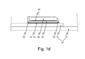
- the second connection partner with its contact surface (56), the power semiconductor device (50), by means of a further adhesive means (60) in its and the edge region of the sinter layer (32) and with contact to the first connection partner, the substrate (10), to be fixed to this.
- Fig. 1d on the left shows an arrangement of the adhesive (60) which extends to the top of the second connection partner, the power semiconductor device (50), while on the right the adhesive (62) is arranged exclusively laterally on the power semiconductor device (50) and otherwise the same on the right side ,
Landscapes
- Engineering & Computer Science (AREA)
- Computer Hardware Design (AREA)
- Microelectronics & Electronic Packaging (AREA)
- Power Engineering (AREA)
- Manufacturing & Machinery (AREA)
- Die Bonding (AREA)
- Powder Metallurgy (AREA)
- Pressure Welding/Diffusion-Bonding (AREA)
- Connections Effected By Soldering, Adhesion, Or Permanent Deformation (AREA)
- Prostheses (AREA)
- Materials For Medical Uses (AREA)
Abstract
Description
Die Erfindung beschreibt ein Herstellungsverfahren zur Niedertemperatur-Drucksinterverbindung zweier Verbindungspartner mit jeweils zu verbindenden Kontaktflächen sowie eine mittels dieses Verfahrens hergestellte Anordnung.The invention describes a production method for the low-temperature pressure sintering connection of two connection partners, each having contact surfaces to be connected, and an arrangement produced by means of this method.
Derartige Anordnungen sind beispielhaft auf dem Gebiet der leistungselektronischen Schaltungen hinlänglich bekannt. Dort werden beispielhaft Leistungshalbleiterbauelemente stoffschlüssig mit Substraten verbunden und in Leistungshalbleitermodulen angeordnet.Such arrangements are well known by way of example in the field of power electronic circuits. There, by way of example, power semiconductor components are materially connected to substrates and arranged in power semiconductor modules.
Beispielhaft beschreibt die
Die bekannten Verfahren weisen allerdings den Nachteil auf, dass das Lösungsmittel erst nach dem Anordnen der Verbindungspartner in der Vorrichtung zur Niedertemperatur- Drucksinterverbindung die Temperaturbeaufschlagung erfolgt und es somit bei der Ausbildung der Verbindung zu Lunkern kommt. Derartige Lunker sind Gaseinschlüsse in der Sintermetallschicht mit einem Durchmesser von mindestens 30µm.However, the known methods have the disadvantage that the solvent only after arranging the connection partner in the device for Low-temperature pressure sintered connection, the temperature is applied and thus it comes to voids in the formation of the compound. Such voids are gas inclusions in the sintered metal layer with a diameter of at least 30 .mu.m.
Der Erfindung liegt die Aufgabe zugrunde ein Herstellungsverfahren und eine hierdurch auszubildende Anordnung mit einer stoffschlüssigen Verbindung in Form einer Niedertemperatur-Drucksinterverbindung zweier Verbindungspartner vorzustellen, wobei die Bildung von Lunkern in der Sintermetallschicht der Niedertemperatur-Drucksinterverbindung verhindert oder zumindest deren Größe wesentlich reduziert wird.The object of the invention is to present a production method and an arrangement to be formed with a material connection in the form of a low-temperature pressure sintered connection of two connection partners, wherein the formation of voids in the sintered metal layer of the low-temperature pressure sintered connection is prevented or at least substantially reduced in size.
Die Aufgabe wird erfindungsgemäß gelöst, durch ein Verfahren mit den Merkmalen des Anspruchs 1, sowie durch eine Anordnung gemäß Anspruch 7. Bevorzugte Ausführungsformen sind in den jeweiligen abhängigen Ansprüchen beschrieben.The object is achieved by a method having the features of claim 1, and by an arrangement according to claim 7. Preferred embodiments are described in the respective dependent claims.
Mittels des erfindungsgemäßen Verfahrens wird eine Anordnung mit einem ersten und einem zweiten Verbindungspartner hergestellt, wobei diese Verbindungspartner mittels einer Niedertemperatur-Drucksinterverbindung stoffschlüssig miteinander verbunden sind. Hierbei weist jeder der Verbindungspartner jeweils eine mit dem anderen Verbindungspartner zu verbindenden Kontaktfläche auf, wobei zwischen diesen Kontaktflächen eine Sintermetallschicht angeordnet ist. Dieses Verfahren umfasst die im Folgenden genannten Schritte. Im Rahmen des erfindungsgemäßen Verfahrens werden die Schritte d) und f) vorteilhafterweise in der genannten Reihenfolge ausgeführt. Es kann allerdings auch bevorzugt sein nur einen der beiden Schritte d) oder f) alternativ auszuführen.
- a) Bereitstellen eines ersten Verbindungspartners mit einer ersten Kontaktfläche, wobei diese vorzugsweise eine Edelmetalloberfläche aufweist. Im Folgenden ist es vorteilhaft, diese Kontaktfläche mittels Einwirkung von Ultraschall von vorhandenen Verunreinigungen zu befreien. Die Einwirkung von Ultraschall kann vor dem nächsten Verfahrensschritt beendet werden, allerdings ist es besonders vorteilhaft um neuerliche Verunreinigungen zu verhindern diese Einwirkung mit dem nächsten Verarbeitungsschritt zeitlich überlappen zu lassen.
- b) Aufbringen einer Schicht aus einer Sinterpaste, bestehend aus Sintermetallpartikeln, vorzugsweise Silberpartikeln, und einem Lösungsmittel, auf die erste Kontaktfläche.
- c) Temperaturbeaufschlagung der Sinterpaste und hierdurch Austreiben des Lösungsmittels unter Bildung der Sinterschicht, die aus noch nicht miteinander verbundenen Sintermetallpartikeln besteht.
- d) Aufbringen einer Flüssigkeit auf der Sinterschicht, wobei diese Flüssigkeit vorzugsweise eine polare Flüssigkeit, wie beispielhaft Glycerin ist. Diese Flüssigkeit dient im nachfolgenden Schritt der Fixierung des zweiten Verbindungspartners auf der Sinterschicht, die nach dem Austreiben des Lösungsmittels nur geringe adhäsive Kräfte zu Fixierung des zweiten Verbindungspartners aufweist.
- e) Anordnen des zweiten Verbindungspartners derart, dass dessen zweite Kontaktfläche auf der Schicht aus Sinterpaste, respektive bei Vorhandensein der Flüssigkeit gemäß Schritt d) präzise ausgedrückt auf dieser, zu liegen kommt.
- f) Anordnen eines Adhäsionsmittels im Randbereich der Sinterschicht und des zweiten Verbindungspartners mit Kontakt des Adhäsionsmittels zum ersten Verbindungspartner zur Fixierung der Verbindungspartner zueinander. Hierbei kann es ausreichend sein das Adhäsionsmittel, das vorzugsweise ein Silikon ist, nur an mindestens zwei einzelnen Stellen der Anordnung aufzubringen. Besonders vorteilhaft ist es allerdings den gesamten beschriebenen Bereich umlaufend mit diesem Adhäsionsmittel zu versehen.
- g) Weitere Beaufschlagung der Anordnung mit Temperatur und Druck zur Ausbildung der stoffschlüssigen Niedertemperatur-Drucksinterverbindung zwischen den Verbindungspartnern. Hierbei wird die Flüssigkeit, die gemäß Schritt d) zwischen der Sinterschicht und dem zweiten Verbindungspartner angeordnet sein kann, ausgetrieben und die Sinterschicht zur homogenen Sintermetallschicht umgewandelt. Unter homogener Sintermetallschicht wird hier eine Metallschicht mit Lunkern verstanden deren maximaler Durchmesser 10µm beträgt.
- a) providing a first connection partner with a first contact surface, which preferably has a noble metal surface. In the following, it is advantageous to free this contact surface by the action of ultrasound of impurities present. The action of ultrasound can be stopped before the next process step, but it is particularly advantageous to prevent further impurities to overlap this action with the next processing step in time.
- b) applying a layer of a sintering paste, consisting of sintered metal particles, preferably silver particles, and a solvent, on the first contact surface.
- c) applying temperature to the sintering paste and thereby expelling the solvent to form the sintered layer, which consists of not yet interconnected sintered metal particles.
- d) applying a liquid to the sintered layer, which liquid is preferably a polar liquid such as glycerin. This liquid is used in the subsequent step, the fixation of the second compound partner on the sintered layer, which has only slight adhesive forces to fix the second connection partner after the expulsion of the solvent.
- e) arranging the second connection partner such that its second contact surface on the layer of sintering paste, or in the presence of the liquid according to step d) comes precisely to lie on this.
- f) arranging an adhesive in the edge region of the sintering layer and the second connection partner with contact of the adhesive to the first connection partner for fixing the connection partner to each other. In this case, it may be sufficient to apply the adhesive, which is preferably a silicone, only to at least two individual locations of the arrangement. However, it is particularly advantageous to provide the entire area described circumferentially with this adhesive.
- g) Further pressurization of the arrangement with temperature and pressure to form the cohesive low-temperature pressure sintered connection between the connection partners. In this case, the liquid which, according to step d), can be arranged between the sintering layer and the second connection partner, is expelled and the sintered layer is converted to the homogeneous sintered metal layer. Homogeneous sintered metal layer is here understood to mean a metal layer with voids whose maximum diameter is 10 μm.
Mittels des beschriebenen erfindungsgemäßen Verfahrens entsteht somit eine Anordnung zweier Verbindungspartner mit einer deren Kontaktflächen verbindenden Sintermetallschicht. Diese Sintermetallschicht ist erfindungsgemäß als homogene Schicht ausgebildet ist weist ausschließlich Lunker mit einem Durchmesser von maximal 10 µm auf.By means of the described method according to the invention thus results in an arrangement of two connection partners with a sintered metal layer connecting their contact surfaces. This sintered metal layer is formed according to the invention as a homogeneous layer has only voids with a maximum diameter of 10 microns.
Der wesentliche Vorteil des erfindungsgemäßen Verfahren bzw. der hierdurch hergestellten erfindungsgemäßen Anordnung ist es, dass durch die geringere Anzahl und / oder geringere Größe der Lunker in der Sintermetallschicht die elektrischen Eigenschaften verbessert, speziell der ohmsche Widerstand verringert, wird und zudem die Dauerhaltbarkeit der Verbindung verbessert wird. Gerade auch in Verbindung mit der der Beaufschlagung durch Ultraschall kann zusätzlich der notwendige Druck zur Ausbildung dieser Verbindung gegenüber dem Stand der Technik um mehr als 10% verringert werden. Jegliche Verringerung des notwendigen und aufzubringenden Druckes erhöht unmittelbar die Ausbeute des Verfahrens, da hierdurch die Bruchrate verringert werden kann.The essential advantage of the method according to the invention or the arrangement produced thereby is that the smaller number and / or smaller size of the voids in the sintered metal layer improves the electrical properties, in particular reduces the ohmic resistance, and also improves the durability of the connection becomes. Especially in connection with the application of ultrasound in addition to the necessary pressure to form this compound over the prior art can be reduced by more than 10%. Any reduction of the necessary and applied pressure immediately increases the yield of the process, as this can reduce the breakage rate.
Die erfinderische Lösung wird an Hand des Ausführungsbeispiels gemäß
Die Kontaktfläche des Substrats mit der der zweite Verbindungspartner in elektrisch leitenden Kontakt gebracht werden soll, weist eine, einer Niedertemperatur-Drucksinterverbindung zugängliche Oberfläche auf. Hierzu ist es bevorzugt, wenn die Kontaktfläche (16) eine Edelmetalloberfläche (18) aufweist. Ebenfalls dargestellt ist eine auf dieser Kontaktfläche (16) angeordnete Sinterpaste (30), die ihrerseits aus Silberpartikeln und einem Lösungsmittel besteht. Im Vorfeld des Aufbringens dieser Sinterpaste (30) wurde begonnen die Oberfläche mit Ultraschall (20) zu beaufschlagen. Diese Beaufschlagung hielt auch während des Aufbringens der Sinterpaste (30) an. Durch diese Maßnahme werden Verunreinigungen, die die spätere Ausbildung der Niedertemperatur-Drucksinterverbindung beeinträchtigen könnten entfernt.The contact surface of the substrate with which the second connection partner is to be brought into electrically conductive contact has a surface accessible to a low-temperature pressure sintering compound. For this purpose, it is preferred if the contact surface (16) has a noble metal surface (18). Also shown is a sintering paste (30) arranged on this contact surface (16), which in turn consists of silver particles and a solvent. Prior to the application of this sintering paste (30) was started to apply the surface with ultrasound (20). This application also continued during the application of the sintering paste (30). By this measure, impurities that could affect the later formation of the low-temperature pressure sintered connection are removed.
Nach diesem Verfahrenschritt liegen von der Sinterpaste (30, gemäß
Um dennoch eine Fixierung des zweiten Verbindungspartners zu erreichen wird, dargestellt in
Alternativ aber besonders bevorzugt zusätzlich zur Fixierung, wie unter
Hierbei kann es ausreichend sein diese Fixierung an zwei oder drei Stellen in dem beschriebenen Randbereich vorzusehen. Falls allerdings eine Fixierung durch die oben beschriebene Flüssigkeit (40) nicht gegeben ist, ist es vorteilhaft dieses Adhäsionsmittel rings um den gesamten Randbereich vorzusehen.It may be sufficient to provide this fixation at two or three points in the described edge region. However, if a fixation by the above-described liquid (40) is not given, it is advantageous to provide this adhesive around the entire edge region.
Bei beiden Ausführungen sind grundsätzlich zwei Varianten gleichwirkend und auch gleichermaßen bevorzugt.
Claims (8)
gekennzeichnet durch diese aufeinander folgenden Schritte, wobei die Schritte d) und f) nacheinander oder alternativ ausgeführt werden können:
characterized by these successive steps, wherein steps d) and f) can be carried out successively or alternatively:
die Flüssigkeit (40) als eine polare Flüssigkeit, vorzugsweise kurzkettige, mehrwertige Alkohole wie Glycerin, ausgebildet ist.The method of claim 1, wherein
the liquid (40) is in the form of a polar liquid, preferably short-chain, polyhydric alcohols, such as glycerol.
das Adhäsionsmittel (60, 62) als ein, vorzugsweise thermisch vernetzendes, Silikon ausgebildet ist.The method of claim 1, wherein
the adhesive (60, 62) is formed as a, preferably thermally crosslinking, silicone.
das Adhäsionsmittel (60, 62) an mindestens zwei Stellen im Randbereich oder umlaufend aufgebracht wird.The method of claim 1, wherein
the adhesive (60, 62) is applied to at least two points in the edge region or circumferentially.
unmittelbar vor Ausführung des Schrittes b) die erste Kontaktfläche (16) und der diese direkt umgebende Bereich mit Ultraschall (20) beaufschlagt wird.The method of claim 1, wherein
Immediately prior to the execution of step b), the first contact surface (16) and the region directly surrounding it are subjected to ultrasound (20).
unmittelbar vor und während der Ausführung des Schrittes b) die erste Kontaktfläche (16) und der diese direkt umgebende Bereich mit Ultraschall (20) beaufschlagt wird.The method of claim 1, wherein
Immediately before and during the execution of step b), the first contact surface (16) and the area directly surrounding it with ultrasound (20) is acted upon.
im Randbereich der Sintermetallschicht (34) ein Adhäsionsmittel (60, 62) vorgesehen ist, das mit beiden Verbindungspartner (10, 50) in Kontakt steht.Arrangement according to claim 7, wherein
in the edge region of the sintered metal layer (34) an adhesive (60, 62) is provided which is in contact with both connection partners (10, 50).
Applications Claiming Priority (1)
| Application Number | Priority Date | Filing Date | Title |
|---|---|---|---|
| DE102010021764.6A DE102010021764B4 (en) | 2010-05-27 | 2010-05-27 | Method for low-temperature pressure sintering of two connection partners |
Publications (2)
| Publication Number | Publication Date |
|---|---|
| EP2390904A2 true EP2390904A2 (en) | 2011-11-30 |
| EP2390904A3 EP2390904A3 (en) | 2014-03-26 |
Family
ID=44774264
Family Applications (1)
| Application Number | Title | Priority Date | Filing Date |
|---|---|---|---|
| EP11162103.3A Withdrawn EP2390904A3 (en) | 2010-05-27 | 2011-04-12 | Method for low temperature pressure interconnection of two connection partners and assembly manufactured using same |
Country Status (4)
| Country | Link |
|---|---|
| EP (1) | EP2390904A3 (en) |
| JP (1) | JP5690652B2 (en) |
| CN (1) | CN102315138B (en) |
| DE (1) | DE102010021764B4 (en) |
Cited By (4)
| Publication number | Priority date | Publication date | Assignee | Title |
|---|---|---|---|---|
| WO2016100470A1 (en) | 2014-12-17 | 2016-06-23 | Alpha Metals, Inc. | Method for die and clip attachment |
| EP3086361A3 (en) * | 2015-04-02 | 2017-01-25 | Heraeus Deutschland GmbH & Co. KG | Method for producing a substrate arrangement with a prefixing means, corresponding substrate arrangement, method for connecting an electronic component with a substrate arrangement using a prefixing means formed on the electronic component and/or the substrate arrangement and an electronic component bonded with a substrate arrangement |
| EP3154079A1 (en) * | 2015-10-08 | 2017-04-12 | Heraeus Deutschland GmbH & Co. KG | Method for connecting a substrate arrangement with an electronic component using a pre-fixing agent on a contact material layer, corresponding substrate arrangement and method of manufacturing thereof |
| DE102015120156A1 (en) * | 2015-11-20 | 2017-05-24 | Semikron Elektronik Gmbh & Co. Kg | Device for material connection of connection partners of a Leistungselekronik component |
Families Citing this family (9)
| Publication number | Priority date | Publication date | Assignee | Title |
|---|---|---|---|---|
| DE102010021765B4 (en) * | 2010-05-27 | 2014-06-12 | Semikron Elektronik Gmbh & Co. Kg | Manufacturing method for the arrangement of two connection partners by means of a low-temperature pressure sintered connection |
| JP2016081943A (en) * | 2014-10-09 | 2016-05-16 | 三菱電機株式会社 | Semiconductor device, and method of manufacturing the same |
| DE102015107724B4 (en) * | 2015-04-02 | 2016-12-01 | Heraeus Deutschland GmbH & Co. KG | Method for producing a substrate arrangement, substrate arrangement, method for connecting an electronic component to a substrate arrangement and electronic component |
| WO2017013808A1 (en) * | 2015-07-23 | 2017-01-26 | ルネサスエレクトロニクス株式会社 | Semiconductor device and method for manufacturing same |
| DE102016124215A1 (en) * | 2016-12-13 | 2018-06-14 | Semikron Elektronik Gmbh & Co. Kg | Process for the low-temperature pressure sintering connection of two connection partners and arrangement produced thereby |
| CN109540374B (en) * | 2019-01-10 | 2024-03-15 | 中南大学 | Ultrasonic sintering packaging device |
| JP7034105B2 (en) * | 2019-01-18 | 2022-03-11 | 三菱電機株式会社 | Manufacturing method of power semiconductor device, power semiconductor device and power conversion device |
| EP3792962A1 (en) * | 2019-09-12 | 2021-03-17 | Infineon Technologies AG | Method for monitoring a process of forming a sinterable connection layer by photometric measurements |
| DE102020103288B3 (en) * | 2020-02-10 | 2020-10-29 | Semikron Elektronik Gmbh & Co. Kg | A method of reducing the surface roughness of a joint surface of a sintered paste layer and pressure sintering method therewith and a sintered joint making device for performing it |
Citations (1)
| Publication number | Priority date | Publication date | Assignee | Title |
|---|---|---|---|---|
| DE102005058794A1 (en) | 2005-12-09 | 2007-06-14 | Semikron Elektronik Gmbh & Co. Kg | Device and clocked process for pressure sintering |
Family Cites Families (13)
| Publication number | Priority date | Publication date | Assignee | Title |
|---|---|---|---|---|
| JPS6245133A (en) * | 1985-08-23 | 1987-02-27 | Hitachi Ltd | Pellet mounting method |
| IN168174B (en) * | 1986-04-22 | 1991-02-16 | Siemens Ag | |
| JPS6436034A (en) * | 1987-07-31 | 1989-02-07 | Nec Corp | Manufacture of semiconductor device |
| EP0460286A3 (en) * | 1990-06-06 | 1992-02-26 | Siemens Aktiengesellschaft | Method and arrangement for bonding a semiconductor component to a substrate or for finishing a semiconductor/substrate connection by contactless pressing |
| JP2950468B2 (en) * | 1996-05-17 | 1999-09-20 | サンケン電気株式会社 | Semiconductor device |
| JP2001176894A (en) * | 1999-12-20 | 2001-06-29 | Nec Yamagata Ltd | Method and device for applying adhesive paste for die bonding |
| DE10009678C1 (en) * | 2000-02-29 | 2001-07-19 | Siemens Ag | Heat conducting adhesive joint between two workpieces used in the production of electronic components comprises a layer of heat conducting material having two flat sided surfaces with openings on each surface |
| JP2006147643A (en) * | 2004-11-16 | 2006-06-08 | Seiko Epson Corp | Bonding method of electronic element, mounting method of electronic element, manufacturing process of electronic device, circuit board, and electronic equipment |
| TWI395253B (en) * | 2004-12-28 | 2013-05-01 | Mitsumasa Koyanagi | Method of fabricating integrated circuit device using self-organization function and apparatus for fabricating same |
| JP4947345B2 (en) * | 2005-11-24 | 2012-06-06 | 三菱マテリアル株式会社 | Method of joining substrate and device using Au-Sn alloy solder paste |
| JP2009164203A (en) * | 2007-12-28 | 2009-07-23 | Mitsubishi Electric Corp | Semiconductor device and manufacturing method of semiconductor device |
| DE102008034946B4 (en) * | 2008-07-26 | 2016-05-19 | Semikron Elektronik Gmbh & Co. Kg | Production method of a noble metal compound |
| DE102008039828A1 (en) * | 2008-08-27 | 2010-03-04 | W.C. Heraeus Gmbh | Control of the porosity of metal pastes for the pressure-free low-temperature sintering process |
-
2010
- 2010-05-27 DE DE102010021764.6A patent/DE102010021764B4/en active Active
-
2011
- 2011-04-12 EP EP11162103.3A patent/EP2390904A3/en not_active Withdrawn
- 2011-05-23 JP JP2011114546A patent/JP5690652B2/en not_active Expired - Fee Related
- 2011-05-27 CN CN201110147129.1A patent/CN102315138B/en not_active Expired - Fee Related
Patent Citations (1)
| Publication number | Priority date | Publication date | Assignee | Title |
|---|---|---|---|---|
| DE102005058794A1 (en) | 2005-12-09 | 2007-06-14 | Semikron Elektronik Gmbh & Co. Kg | Device and clocked process for pressure sintering |
Cited By (12)
| Publication number | Priority date | Publication date | Assignee | Title |
|---|---|---|---|---|
| WO2016100470A1 (en) | 2014-12-17 | 2016-06-23 | Alpha Metals, Inc. | Method for die and clip attachment |
| EP3234988A4 (en) * | 2014-12-17 | 2018-09-12 | Alpha Assembly Solutions Inc. | Method for die and clip attachment |
| US11289447B2 (en) | 2014-12-17 | 2022-03-29 | Alpha Assembly Solutions, Inc. | Method for die and clip attachment |
| EP3086361A3 (en) * | 2015-04-02 | 2017-01-25 | Heraeus Deutschland GmbH & Co. KG | Method for producing a substrate arrangement with a prefixing means, corresponding substrate arrangement, method for connecting an electronic component with a substrate arrangement using a prefixing means formed on the electronic component and/or the substrate arrangement and an electronic component bonded with a substrate arrangement |
| EP3154079A1 (en) * | 2015-10-08 | 2017-04-12 | Heraeus Deutschland GmbH & Co. KG | Method for connecting a substrate arrangement with an electronic component using a pre-fixing agent on a contact material layer, corresponding substrate arrangement and method of manufacturing thereof |
| WO2017060140A3 (en) * | 2015-10-08 | 2017-06-01 | Heraeus Deutschland GmbH & Co. KG | Method for connecting a substrate arrangement to an electronic component using a pre-fixation agent applied onto a contacting material layer, corresponding substrate arrangement, and method for producing same |
| US20180286831A1 (en) * | 2015-10-08 | 2018-10-04 | Heraeus Deutschland GmbH & Co. KG | Method for producing a substrate arrangement, substrate arrangement, and method for connecting a substrate arrangement to an electronic component |
| US10622331B2 (en) | 2015-10-08 | 2020-04-14 | Heraeus Deutschland GmbH & Co. KG | Method for producing a substrate arrangement, substrate arrangement, and method for connecting a substrate arrangement to an electronic component |
| EP3940758A3 (en) * | 2015-10-08 | 2022-08-10 | Heraeus Deutschland GmbH & Co. KG | Method for connecting a substrate arrangement with an electronic component by sintering using a pre-fixing agent on a sintering contact material layer, corresponding substrate arrangement and method of manufacturing thereof |
| DE102015120156A1 (en) * | 2015-11-20 | 2017-05-24 | Semikron Elektronik Gmbh & Co. Kg | Device for material connection of connection partners of a Leistungselekronik component |
| DE102015120156B4 (en) * | 2015-11-20 | 2019-07-04 | Semikron Elektronik Gmbh & Co. Kg | Device for the material connection of connection partners of a Leistungselekronik component and use of such a device |
| US10603741B2 (en) | 2015-11-20 | 2020-03-31 | Semikron Elektronik Gmbh & Co., Kg | Apparatus for the material-bonded connection of connection partners of a power-electronics component |
Also Published As
| Publication number | Publication date |
|---|---|
| JP5690652B2 (en) | 2015-03-25 |
| CN102315138B (en) | 2016-03-02 |
| EP2390904A3 (en) | 2014-03-26 |
| JP2011249801A (en) | 2011-12-08 |
| DE102010021764B4 (en) | 2014-09-25 |
| CN102315138A (en) | 2012-01-11 |
| DE102010021764A1 (en) | 2011-12-01 |
Similar Documents
| Publication | Publication Date | Title |
|---|---|---|
| DE102010021764B4 (en) | Method for low-temperature pressure sintering of two connection partners | |
| DE102010021765B4 (en) | Manufacturing method for the arrangement of two connection partners by means of a low-temperature pressure sintered connection | |
| EP3970210A1 (en) | Method for producing a display having a carrier substrate, a carrier substrate produced according to said method, and a cover glass intended for a flexible display | |
| DE102007054710B3 (en) | Method for producing a semiconductor module | |
| DE102007022337A1 (en) | Sintered power semiconductor substrate and manufacturing method thereof | |
| DE102012207652A1 (en) | Two-stage process for joining a semiconductor to a substrate with silver-based compound material | |
| WO2013013964A1 (en) | Carrier device, electrical device having a carrier device and method for producing same | |
| EP3026702B1 (en) | Method of producing a semiconductor element with substrate adapter and semiconductor element with substrate adapter | |
| DE19522338B4 (en) | Chip carrier assembly with a via | |
| EP2713685A2 (en) | Method for creating a soldered connection and circuit component | |
| DE102009024371B4 (en) | Method for producing a converter arrangement with cooling device and converter arrangement | |
| DE102013200868B4 (en) | Process for producing a material connection and an electrical connection | |
| DE102010001666A1 (en) | Electrical or electronic composite component e.g. junction FET (JFET) has connection layer and interlayer whose active compound is arranged on attaching layers along opposite side of sinter layers | |
| EP1993132B1 (en) | High performance semiconductor substrate with metal contact layer and corresponding production method | |
| DE102009040627B4 (en) | Semiconductor device and method of manufacturing an electronic system | |
| DE102008034946B4 (en) | Production method of a noble metal compound | |
| DE102011005322B4 (en) | Method for producing a power semiconductor substrate | |
| EP2146372A2 (en) | Power electronic connection device and production method for same | |
| DE102007022338B4 (en) | Manufacturing method for a power semiconductor device with metal contact layer | |
| DE102015107712B3 (en) | Method for producing a circuit carrier | |
| DE102018221148A1 (en) | Method for producing a substrate adapter and substrate adapter for connecting to an electronic component | |
| DE102013111748A1 (en) | Solar module and solar module manufacturing process | |
| DE102009017692B4 (en) | Process for the production of a low temperature contact for microelectronic structures | |
| DE102014106763B4 (en) | Method for producing a semiconductor module | |
| DE102016124215A1 (en) | Process for the low-temperature pressure sintering connection of two connection partners and arrangement produced thereby |
Legal Events
| Date | Code | Title | Description |
|---|---|---|---|
| AK | Designated contracting states |
Kind code of ref document: A2 Designated state(s): AL AT BE BG CH CY CZ DE DK EE ES FI FR GB GR HR HU IE IS IT LI LT LU LV MC MK MT NL NO PL PT RO RS SE SI SK SM TR |
|
| AX | Request for extension of the european patent |
Extension state: BA ME |
|
| PUAI | Public reference made under article 153(3) epc to a published international application that has entered the european phase |
Free format text: ORIGINAL CODE: 0009012 |
|
| RIC1 | Information provided on ipc code assigned before grant |
Ipc: H01L 21/60 20060101AFI20131029BHEP Ipc: H01L 23/488 20060101ALI20131029BHEP |
|
| PUAL | Search report despatched |
Free format text: ORIGINAL CODE: 0009013 |
|
| AK | Designated contracting states |
Kind code of ref document: A3 Designated state(s): AL AT BE BG CH CY CZ DE DK EE ES FI FR GB GR HR HU IE IS IT LI LT LU LV MC MK MT NL NO PL PT RO RS SE SI SK SM TR |
|
| AX | Request for extension of the european patent |
Extension state: BA ME |
|
| RIC1 | Information provided on ipc code assigned before grant |
Ipc: H01L 23/488 20060101ALI20140214BHEP Ipc: H01L 21/60 20060101AFI20140214BHEP |
|
| STAA | Information on the status of an ep patent application or granted ep patent |
Free format text: STATUS: THE APPLICATION HAS BEEN WITHDRAWN |
|
| 18W | Application withdrawn |
Effective date: 20140911 |