DE19522338B4 - Chip carrier assembly with a via - Google Patents
Chip carrier assembly with a via Download PDFInfo
- Publication number
- DE19522338B4 DE19522338B4 DE19522338A DE19522338A DE19522338B4 DE 19522338 B4 DE19522338 B4 DE 19522338B4 DE 19522338 A DE19522338 A DE 19522338A DE 19522338 A DE19522338 A DE 19522338A DE 19522338 B4 DE19522338 B4 DE 19522338B4
- Authority
- DE
- Germany
- Prior art keywords
- chip
- substrate
- metallization
- metallization layers
- chip carrier
- Prior art date
- Legal status (The legal status is an assumption and is not a legal conclusion. Google has not performed a legal analysis and makes no representation as to the accuracy of the status listed.)
- Expired - Lifetime
Links
Classifications
-
- H—ELECTRICITY
- H01—ELECTRIC ELEMENTS
- H01L—SEMICONDUCTOR DEVICES NOT COVERED BY CLASS H10
- H01L21/00—Processes or apparatus adapted for the manufacture or treatment of semiconductor or solid state devices or of parts thereof
- H01L21/02—Manufacture or treatment of semiconductor devices or of parts thereof
- H01L21/04—Manufacture or treatment of semiconductor devices or of parts thereof the devices having at least one potential-jump barrier or surface barrier, e.g. PN junction, depletion layer or carrier concentration layer
- H01L21/48—Manufacture or treatment of parts, e.g. containers, prior to assembly of the devices, using processes not provided for in a single one of the subgroups H01L21/06 - H01L21/326
- H01L21/4814—Conductive parts
- H01L21/4846—Leads on or in insulating or insulated substrates, e.g. metallisation
- H01L21/486—Via connections through the substrate with or without pins
-
- H—ELECTRICITY
- H01—ELECTRIC ELEMENTS
- H01L—SEMICONDUCTOR DEVICES NOT COVERED BY CLASS H10
- H01L21/00—Processes or apparatus adapted for the manufacture or treatment of semiconductor or solid state devices or of parts thereof
- H01L21/02—Manufacture or treatment of semiconductor devices or of parts thereof
- H01L21/04—Manufacture or treatment of semiconductor devices or of parts thereof the devices having at least one potential-jump barrier or surface barrier, e.g. PN junction, depletion layer or carrier concentration layer
- H01L21/48—Manufacture or treatment of parts, e.g. containers, prior to assembly of the devices, using processes not provided for in a single one of the subgroups H01L21/06 - H01L21/326
- H01L21/4814—Conductive parts
- H01L21/4846—Leads on or in insulating or insulated substrates, e.g. metallisation
- H01L21/4853—Connection or disconnection of other leads to or from a metallisation, e.g. pins, wires, bumps
-
- H—ELECTRICITY
- H05—ELECTRIC TECHNIQUES NOT OTHERWISE PROVIDED FOR
- H05K—PRINTED CIRCUITS; CASINGS OR CONSTRUCTIONAL DETAILS OF ELECTRIC APPARATUS; MANUFACTURE OF ASSEMBLAGES OF ELECTRICAL COMPONENTS
- H05K3/00—Apparatus or processes for manufacturing printed circuits
- H05K3/40—Forming printed elements for providing electric connections to or between printed circuits
- H05K3/4038—Through-connections; Vertical interconnect access [VIA] connections
- H05K3/4084—Through-connections; Vertical interconnect access [VIA] connections by deforming at least one of the conductive layers
-
- H—ELECTRICITY
- H05—ELECTRIC TECHNIQUES NOT OTHERWISE PROVIDED FOR
- H05K—PRINTED CIRCUITS; CASINGS OR CONSTRUCTIONAL DETAILS OF ELECTRIC APPARATUS; MANUFACTURE OF ASSEMBLAGES OF ELECTRICAL COMPONENTS
- H05K2201/00—Indexing scheme relating to printed circuits covered by H05K1/00
- H05K2201/03—Conductive materials
- H05K2201/0332—Structure of the conductor
- H05K2201/0388—Other aspects of conductors
- H05K2201/0394—Conductor crossing over a hole in the substrate or a gap between two separate substrate parts
-
- H—ELECTRICITY
- H05—ELECTRIC TECHNIQUES NOT OTHERWISE PROVIDED FOR
- H05K—PRINTED CIRCUITS; CASINGS OR CONSTRUCTIONAL DETAILS OF ELECTRIC APPARATUS; MANUFACTURE OF ASSEMBLAGES OF ELECTRICAL COMPONENTS
- H05K2201/00—Indexing scheme relating to printed circuits covered by H05K1/00
- H05K2201/09—Shape and layout
- H05K2201/09209—Shape and layout details of conductors
- H05K2201/095—Conductive through-holes or vias
- H05K2201/09509—Blind vias, i.e. vias having one side closed
-
- H—ELECTRICITY
- H05—ELECTRIC TECHNIQUES NOT OTHERWISE PROVIDED FOR
- H05K—PRINTED CIRCUITS; CASINGS OR CONSTRUCTIONAL DETAILS OF ELECTRIC APPARATUS; MANUFACTURE OF ASSEMBLAGES OF ELECTRICAL COMPONENTS
- H05K2203/00—Indexing scheme relating to apparatus or processes for manufacturing printed circuits covered by H05K3/00
- H05K2203/01—Tools for processing; Objects used during processing
- H05K2203/0195—Tool for a process not provided for in H05K3/00, e.g. tool for handling objects using suction, for deforming objects, for applying local pressure
-
- H—ELECTRICITY
- H05—ELECTRIC TECHNIQUES NOT OTHERWISE PROVIDED FOR
- H05K—PRINTED CIRCUITS; CASINGS OR CONSTRUCTIONAL DETAILS OF ELECTRIC APPARATUS; MANUFACTURE OF ASSEMBLAGES OF ELECTRICAL COMPONENTS
- H05K2203/00—Indexing scheme relating to apparatus or processes for manufacturing printed circuits covered by H05K3/00
- H05K2203/02—Details related to mechanical or acoustic processing, e.g. drilling, punching, cutting, using ultrasound
- H05K2203/0285—Using ultrasound, e.g. for cleaning, soldering or wet treatment
-
- H—ELECTRICITY
- H05—ELECTRIC TECHNIQUES NOT OTHERWISE PROVIDED FOR
- H05K—PRINTED CIRCUITS; CASINGS OR CONSTRUCTIONAL DETAILS OF ELECTRIC APPARATUS; MANUFACTURE OF ASSEMBLAGES OF ELECTRICAL COMPONENTS
- H05K2203/00—Indexing scheme relating to apparatus or processes for manufacturing printed circuits covered by H05K3/00
- H05K2203/10—Using electric, magnetic and electromagnetic fields; Using laser light
- H05K2203/107—Using laser light
-
- H—ELECTRICITY
- H05—ELECTRIC TECHNIQUES NOT OTHERWISE PROVIDED FOR
- H05K—PRINTED CIRCUITS; CASINGS OR CONSTRUCTIONAL DETAILS OF ELECTRIC APPARATUS; MANUFACTURE OF ASSEMBLAGES OF ELECTRICAL COMPONENTS
- H05K2203/00—Indexing scheme relating to apparatus or processes for manufacturing printed circuits covered by H05K3/00
- H05K2203/11—Treatments characterised by their effect, e.g. heating, cooling, roughening
- H05K2203/1189—Pressing leads, bumps or a die through an insulating layer
-
- H—ELECTRICITY
- H05—ELECTRIC TECHNIQUES NOT OTHERWISE PROVIDED FOR
- H05K—PRINTED CIRCUITS; CASINGS OR CONSTRUCTIONAL DETAILS OF ELECTRIC APPARATUS; MANUFACTURE OF ASSEMBLAGES OF ELECTRICAL COMPONENTS
- H05K2203/00—Indexing scheme relating to apparatus or processes for manufacturing printed circuits covered by H05K3/00
- H05K2203/15—Position of the PCB during processing
- H05K2203/1572—Processing both sides of a PCB by the same process; Providing a similar arrangement of components on both sides; Making interlayer connections from two sides
Abstract
Chipträgeranordnung mit einem Chip und einem Chipträger aus einem verformbaren Substrat, das mit einer dem Chip zugewandten Chipkontaktseite auf der mit Anschlussflächen versehenen Oberseite des Chips angeordnet ist und im Bereich der Anschlussflächen auf der Gegenseite Metallisierungslagen aufweist, die mit den Anschlussflächen des Chips verbunden sind, dadurch gekennzeichnet, dass die Kontaktierung der Metallisierungslagen (36) mit den Anschlussflächen (39) vermittels Durchkontaktierungen (37, 38) gebildet ist, die durch eine während der Kontaktierung erfolgte Verdrängung anfänglich geschlossen ausgebildeter Substratbereiche in Folge einer einwärts gerichteten Verformung nicht durchstoßener Bereiche der Metallisierungslagen (36) gebildet sind, wobei das Substrat nur auf einer Seite Metallisierungslagen aufweist und das Substrat abseits von den Bereichen der Durchkontaktierungen im Wesentlichen unverformt ist.Chip carrier assembly with a chip and a chip carrier from a deformable substrate facing the chip Chip contact side on the provided with pads top of Chips is arranged and in the area of the connection surfaces on the Has metallization layers on the opposite side, with the pads of the Chips are connected, characterized in that the contacting the metallization layers (36) with the connection surfaces (39) by means of vias (37, 38) is formed by one during the contacting was done repression initially closed formed substrate areas due to an inwardly directed Deformation not pierced Areas of the metallization layers (36) are formed, wherein the Substrate has only on one side metallization and the Substrate away from the areas of the vias substantially is undeformed.
Description
Die vorliegende Erfindung Chipträgeranordnung gemäß dem Oberbegriff des Anspruchs 1.The present invention chip carrier assembly according to the generic term of claim 1.
Substrate, die zur Bestückung mit elektronischen Bauelementen dienen, sind in der Regel mit sogenannten Durchkontaktierungen versehen, die auf gegenüberliegenden Oberflächen des Substrats angeordnete Leiterbahnstrukturen zur Erzielung einer höheren Integration miteinander verbinden. Derartige Substrat-Durchkontaktierungen gewinnen aufgrund der zunehmenden Integration im Schaltungsaufbau bis hin zu sogenannten "Multi-Layer-Modulen", bei denen mehrere bestückte Substrate in Schichttechnik aufeinander angeordnet sind, zunehmend an Bedeutung.substrates the for fitting Serve with electronic components are usually with so-called Vias provided on opposite surfaces of the Substrate arranged conductor track structures to achieve a higher integration connect with each other. Such substrate vias gain due to the increasing integration in the circuit construction up to to so-called "multi-layer modules" in which several stocked Substrates are arranged in layered technology, increasingly in importance.
Der Herstellungsaufwand bei Substraten, die mit Durchkontaktierungen versehen sind, wird wesentlich durch den Aufwand zur Herstellung der eigentlichen Durchkontaktierungen bestimmt. Bei den bekannten Verfahren zur Herstellung einer Durchkontaktierung werden die auf gegenüberliegenden Oberflächen mit Leiterbahnstrukturen versehenen Substrate an den Durchkontaktierungsstellen durchbohrt oder geätzt, um anschließend den derart geschaffenen Durchgang auf galvanischem oder chemischem Wege zur Herstellung einer elektrisch leitfähigen Verbindung zwischen den Leiterbahnstrukturen metallisch auszukleiden. Daher sind die bekannten Verfahren zeitaufwendig und mit entsprechend hohen Investitionskosten zur Bereitstellung der notwendigen Herstellungseinrichtungen verbunden. Dies wirkt insbesondere einer weiteren Entwicklung der Multi-Layer-Technik entgegen.Of the Production cost for substrates with vias are provided, is essential by the effort to produce determined the actual vias. In the known Methods for producing a via are the on with opposite surfaces Conductor structures provided substrates at the via sites pierced or etched, then the thus created passage by galvanic or chemical means for producing an electrically conductive connection between the Metallic strip conductor structures. Therefore, the known Time-consuming process and with correspondingly high investment costs connected to provide the necessary manufacturing facilities. This In particular, it affects the further development of multi-layer technology opposite.
In der deutschen Auslegeschrift 1 640 468 wird ein Verfahren zur elektrischen Verbindung von vorgefertigten Leiterbahnanordnungen, welche sich auf gegenüberliegenden Seiten der Leiterplatte befinden, vorgeschlagen. Die Ausbildung der Leiterbahnanordnung erfolgt dabei vor der Durchführung der Durchkontaktierung. Die Kontaktierung erfolgt durch ein Eindrücken einer Metallisierungslage gegen die andere mit Hilfe eines Stempels. Zur sicheren elektrischen Kontaktierung ist anschließend noch ein Plattieren der derart ausgeformten Lochungen erforderlich.In German Auslegeschrift 1 640 468 is a method for electrical Connection of prefabricated conductor arrangement, which is based on opposite Pages of the circuit board are proposed. Training the conductor track arrangement takes place before the implementation of Via. The contact is made by pressing a Metallization layer against the other with the help of a punch. to secure electrical contact is then a plating of the such shaped perforations required.
In
der amerikanischen Patentschrift
In der japanischen Druckschrift JP 3-201498 (A) ist ein Verfahren beschrieben, bei dem eine durch eine Isolierschicht von einer Metallplatte getrennte, vorab ausgebildete Leiterbahnstruktur durch einen Stempel, welcher die beiden leitenden Schichten unter Verdrängung der Isolierschicht zusammenpresst, elektrisch miteinander verbunden werden.In Japanese Patent Publication JP 3-201498 (A) describes a method in which one separated by an insulating layer of a metal plate, in advance Traced conductor track structure by a stamp, which the two conductive layers pressed together to displace the insulating layer, electrically be connected to each other.
In der japanischen Druckschrift JP 3-30494 (A)1 ist ein Verfahren zur elektrischen Verbindung zweier Metallfolien, welche sich aufeinander gegenüberliegender Seiten eines Isolierträgers befinden, beschrieben. Die Verbindung erfolgt durch ultraschallbeaufschlagte Stempel, welche die Metallfolien im Bereich der Durchkontaktierungsstelle zusammendrücken. Um eine gute elektrische Verbindung zu garantieren, ist der Isolierträger mit elektrisch leitenden Teilchen versetzt.In Japanese Patent Publication JP 3-30494 (A) 1 is a method for electrical connection of two metal foils which overlap one another opposed Pages of an insulated vehicle are described. The connection is made by ultrasonically charged Stamp, which the metal foils in the region of the Durchkontaktierungsstelle Squeeze. To ensure a good electrical connection, the insulated support is electrically conductive particles added.
In
der europäischen
Patentschrift
In
der amerikanischen Patentschrift
Aus
der
Der vorliegenden Erfindung liegt die Aufgabe zugrunde, eine Chipträgeranordnung unter Verwendung eines Substrats bereitzustellen, das mit geringem Aufwand herstellbare Durchkontaktierungen aufweist.Of the The present invention is based on the object, a chip carrier assembly using a substrate that has low Has cost producible vias.
Diese Aufgabe wird durch eine Chipträgeranordnung mit den Merkmalen des Anspruchs 1 gelöst.These Task is by a chip carrier assembly solved with the features of claim 1.
Bei der erfindungsgemäßen Chipträgeranordnung erfolgt die Substratverdrängung ausschließlich während der Kontaktierung in Folge einer einwärts gerichteten Verformung nicht durchstoßener Bereiche der Metallisierungslagen.at the chip carrier assembly according to the invention the substrate displacement takes place exclusively while contacting as a result of inward deformation not pierced areas the metallization layers.
Dabei können die verformten Bereiche der Metallisierungslagen je nach Materialbeschaffenheit unmittelbar mit den Anschlussflächen des Chips oder über zuvor als Verbindungsmedium auf die Anschlussflächen des Chips aufgebrachte Kontaktmetallisierungen, die verbindungskompatibel mit dem Material der Metallisierungslagen sind, mit den Chip-Anschlussflächen verbunden sein.there can the deformed areas of the metallization layers, depending on the nature of the material immediately with the connection surfaces of the chip or over previously applied as a bonding medium on the pads of the chip Contact metallizations that are compound compatible with the material the metallization layers are connected to the chip pads.
Bevorzugte Ausführungsformen des erfindungsgemäßen Verfahrens sowie Ausführungsbeispiele für einen durch Anwendung des Verfahrens hergestellten Chipträger bzw. eine Chipträgeranordnung werden unter Bezugnahme auf die beiliegenden Zeichnungen nachfolgend näher erläutert. Es zeigen:preferred embodiments the method according to the invention as well as exemplary embodiments for one Chip carrier manufactured by using the method or a chip carrier arrangement will be described below with reference to the accompanying drawings explained in more detail. Show it:
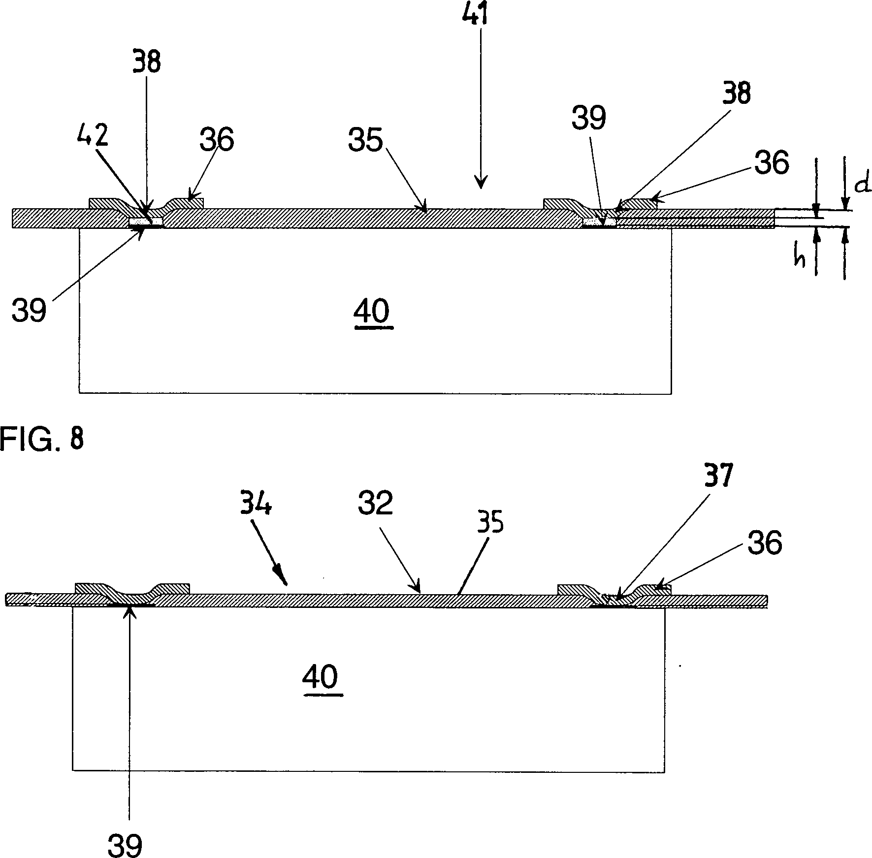
Die
Metallisierungslagen
Zur
Herstellung der Durchkontaktierung
Gleichzeitig
mit der plastischen Verformung der Metallisierungslage
Bei
der in
Bei
der in
Durch
die Wärmebeaufschlagung
der oberen Metallisierungslage
Bei
den in
In
den
Ausgehend
von einer in
Bezüglich der
Verformungsvorgänge
der Metallisierungslagen
Die
in den
In
seiner Ausgangsform besteht der in
Die
Darstellung in
Ein
zwischen der Oberfläche
des Chips
Zur
Herstellung der Durchkontaktierungen
Die
in den
Die
in den
Claims (1)
Priority Applications (1)
| Application Number | Priority Date | Filing Date | Title |
|---|---|---|---|
| DE19522338A DE19522338B4 (en) | 1995-06-20 | 1995-06-20 | Chip carrier assembly with a via |
Applications Claiming Priority (1)
| Application Number | Priority Date | Filing Date | Title |
|---|---|---|---|
| DE19522338A DE19522338B4 (en) | 1995-06-20 | 1995-06-20 | Chip carrier assembly with a via |
Publications (2)
| Publication Number | Publication Date |
|---|---|
| DE19522338A1 DE19522338A1 (en) | 1997-01-02 |
| DE19522338B4 true DE19522338B4 (en) | 2006-12-07 |
Family
ID=7764772
Family Applications (1)
| Application Number | Title | Priority Date | Filing Date |
|---|---|---|---|
| DE19522338A Expired - Lifetime DE19522338B4 (en) | 1995-06-20 | 1995-06-20 | Chip carrier assembly with a via |
Country Status (1)
| Country | Link |
|---|---|
| DE (1) | DE19522338B4 (en) |
Families Citing this family (16)
| Publication number | Priority date | Publication date | Assignee | Title |
|---|---|---|---|---|
| US6005198A (en) * | 1997-10-07 | 1999-12-21 | Dimensional Circuits Corporation | Wiring board constructions and methods of making same |
| WO1999049708A1 (en) * | 1998-03-27 | 1999-09-30 | Minnesota Mining And Manufacturing Company | Method for making electrical connections between conductors separated by a dielectric |
| EP1009023A1 (en) * | 1998-12-09 | 2000-06-14 | ESEC Management SA | Method for connecting two conductor structures and resin object |
| FR2793432B1 (en) | 1999-05-10 | 2001-07-06 | Gemplus Card Int | METHOD FOR PRODUCING A CONTACT BETWEEN TWO CONDUCTIVE LAYERS SEPARATED BY AN INSULATING LAYER |
| US6583364B1 (en) * | 1999-08-26 | 2003-06-24 | Sony Chemicals Corp. | Ultrasonic manufacturing apparatuses, multilayer flexible wiring boards and processes for manufacturing multilayer flexible wiring boards |
| WO2001080612A1 (en) * | 2000-03-31 | 2001-10-25 | Dyconex Patente Ag | Method for fabricating electrical connecting element, and electrical connecting element |
| AU2001242204A1 (en) * | 2000-03-31 | 2001-10-23 | Dyconex Patente Ag | Method and device for fabricating electrical connecting elements, and connectingelement |
| US20030121146A1 (en) * | 2000-03-31 | 2003-07-03 | Walter Schmidt | Method for fabricating electrical connecting elements, and connecting element |
| DE10122414A1 (en) * | 2001-05-09 | 2002-11-14 | Giesecke & Devrient Gmbh | Through connection of flexible printed circuit boards |
| DE10202145A1 (en) * | 2002-01-21 | 2003-05-08 | Siemens Dematic Ag | Production of connecting substrates comprises laminating substrate film made from polymer with metal layer on one side, forming bumps and recesses on one side of the substrate foil, covering the surface with metal layer and structuring |
| DE10205521A1 (en) * | 2002-02-08 | 2003-08-28 | Heraeus Gmbh W C | Process for the electrical contacting of two metal structures |
| WO2004027866A2 (en) * | 2002-09-23 | 2004-04-01 | Johnson Controls Technology Company | Method for creating a link in an integrated metal substrate |
| US7511371B2 (en) | 2005-11-01 | 2009-03-31 | Sandisk Corporation | Multiple die integrated circuit package |
| US7352058B2 (en) | 2005-11-01 | 2008-04-01 | Sandisk Corporation | Methods for a multiple die integrated circuit package |
| EP1949440A2 (en) * | 2005-11-01 | 2008-07-30 | SanDisk Corporation | Multiple die integrated circuit package |
| AU2010243050B2 (en) * | 2009-04-28 | 2014-09-11 | Toppan Printing Co., Ltd. | Antenna sheet, data carrier with non-contact IC, and method for manufacturing antenna sheet |
Citations (8)
| Publication number | Priority date | Publication date | Assignee | Title |
|---|---|---|---|---|
| US3037265A (en) * | 1957-12-30 | 1962-06-05 | Ibm | Method for making printed circuits |
| US3155809A (en) * | 1964-04-21 | 1964-11-03 | Digital Sensors Inc | Means and techniques for making electrical connections |
| DE1640468B2 (en) * | 1965-06-16 | 1971-06-03 | ELECTRICAL CONNECTION BETWEEN OPERATING SIDES OF CIRCUIT BOARDS | |
| JPH0330494A (en) * | 1989-06-28 | 1991-02-08 | Sharp Corp | Through-hole forming method for flexible circuit board |
| JPH03201498A (en) * | 1989-12-28 | 1991-09-03 | Matsushita Electric Ind Co Ltd | Metal board interconnection |
| EP0343400B1 (en) * | 1988-05-26 | 1994-03-16 | International Business Machines Corporation | Electronic package assembly with flexible carrier and method of making it |
| US5346861A (en) * | 1990-09-24 | 1994-09-13 | Tessera, Inc. | Semiconductor chip assemblies and methods of making same |
| US5398863A (en) * | 1993-07-23 | 1995-03-21 | Tessera, Inc. | Shaped lead structure and method |
-
1995
- 1995-06-20 DE DE19522338A patent/DE19522338B4/en not_active Expired - Lifetime
Patent Citations (8)
| Publication number | Priority date | Publication date | Assignee | Title |
|---|---|---|---|---|
| US3037265A (en) * | 1957-12-30 | 1962-06-05 | Ibm | Method for making printed circuits |
| US3155809A (en) * | 1964-04-21 | 1964-11-03 | Digital Sensors Inc | Means and techniques for making electrical connections |
| DE1640468B2 (en) * | 1965-06-16 | 1971-06-03 | ELECTRICAL CONNECTION BETWEEN OPERATING SIDES OF CIRCUIT BOARDS | |
| EP0343400B1 (en) * | 1988-05-26 | 1994-03-16 | International Business Machines Corporation | Electronic package assembly with flexible carrier and method of making it |
| JPH0330494A (en) * | 1989-06-28 | 1991-02-08 | Sharp Corp | Through-hole forming method for flexible circuit board |
| JPH03201498A (en) * | 1989-12-28 | 1991-09-03 | Matsushita Electric Ind Co Ltd | Metal board interconnection |
| US5346861A (en) * | 1990-09-24 | 1994-09-13 | Tessera, Inc. | Semiconductor chip assemblies and methods of making same |
| US5398863A (en) * | 1993-07-23 | 1995-03-21 | Tessera, Inc. | Shaped lead structure and method |
Non-Patent Citations (6)
| Title |
|---|
| HUMMEL,Manfred: Einführung in die Leiterplatten- technologie. Saulgau: Eugen G. Leuze Verlag, 1991. ISBN: 3-87480-068-7, S.91 und 109 |
| HUMMEL,Manfred: Einführung in die Leiterplatten- technologie. Saulgau: Eugen G. Leuze Verlag, 1991.ISBN: 3-87480-068-7, S.91 und 109 * |
| JP Pat.Abstr. E-1059, April 22, 1991, Vol. 15/ No. 159 & JP 03030494 A * |
| JP Pat.Abstr. E-1059, April 22, 1991, Vol. 15/ No. 159 & JP 3-30494 A |
| JP Pat.Abstr. E-1138, Nov. 26, 1991, Vol. 15/ No. 465 & JP 03201498 A * |
| JP Pat.Abstr. E-1138, Nov. 26, 1991, Vol. 15/ No. 465 & JP 3-201498 A |
Also Published As
| Publication number | Publication date |
|---|---|
| DE19522338A1 (en) | 1997-01-02 |
Similar Documents
| Publication | Publication Date | Title |
|---|---|---|
| DE19522338B4 (en) | Chip carrier assembly with a via | |
| DE3818894C2 (en) | ||
| DE112004001727B4 (en) | Method of manufacturing an electronic module | |
| DE69938582T2 (en) | SEMICONDUCTOR ELEMENT, ITS MANUFACTURE, PCB AND ELECTRONIC APPARATUS | |
| EP2259311B1 (en) | Method for embedding at least one component into a circuit board element | |
| DE102007058497B4 (en) | Multilayer printed circuit board and method for producing a multilayer printed circuit board | |
| DE69233232T2 (en) | Electrical connector body and manufacturing method therefor | |
| DE102014213083B4 (en) | Bond structure with metal nanoparticles and bonding process using metal nanoparticles | |
| DE3125518A1 (en) | "Thin wiring arrangement" | |
| DE19848834A1 (en) | Applying integrated circuit flip-chip to substrate | |
| DE112008003532T5 (en) | A method of manufacturing a multi-layer wiring substrate | |
| DE102009043587A1 (en) | Functional laminate | |
| DE10291877T5 (en) | Connector, microswitch, method of manufacturing a connector and method of manufacturing a microswitch | |
| DE102006036728B4 (en) | Method for the electrical contacting of microelectronic components on a printed circuit board | |
| EP0610360A1 (en) | Process for manufacturing a printed circuit and printed circuit. | |
| DE4424831C2 (en) | Process for producing an electrically conductive connection | |
| DE4327560A1 (en) | Method for connecting interconnection arrangements and contact arrangement | |
| DE60130108T2 (en) | METHOD FOR PRODUCING ELECTRICAL CONNECTING ELEMENTS AND CONNECTING ELEMENT | |
| DE102005027276B3 (en) | Production process for a stack of at least two base materials comprising printed circuit boards photostructures the boards applies solder stacks and melts with lacquer separating the boards | |
| EP1116180B1 (en) | Method for contacting a circuit chip | |
| DE2805535A1 (en) | METHOD FOR ESTABLISHING A CONDUCTIVE CONNECTION THROUGH AN ELECTRONIC CIRCUIT BOARD | |
| DE10007414B4 (en) | Process for the through-plating of a substrate for power semiconductor modules by solder and substrate produced by the method | |
| WO1997008925A1 (en) | Method of establishing a connection between at least two electrical conductors, one of which is mounted on a supporting substrate | |
| DE10304777B4 (en) | Method for producing a chip using a heat and pressure process using a thermoplastic material and apparatus for carrying out the method | |
| DE10133959B4 (en) | Electronic component with semiconductor chip |
Legal Events
| Date | Code | Title | Description |
|---|---|---|---|
| OP8 | Request for examination as to paragraph 44 patent law | ||
| 8127 | New person/name/address of the applicant |
Owner name: PAC TECH - PACKAGING TECHNOLOGIES GMBH, 14641 NAUE |
|
| 8364 | No opposition during term of opposition | ||
| R071 | Expiry of right |