CN203617293U - Diode module assembly for rectifier circuit - Google Patents
Diode module assembly for rectifier circuit Download PDFInfo
- Publication number
- CN203617293U CN203617293U CN201320836850.6U CN201320836850U CN203617293U CN 203617293 U CN203617293 U CN 203617293U CN 201320836850 U CN201320836850 U CN 201320836850U CN 203617293 U CN203617293 U CN 203617293U
- Authority
- CN
- China
- Prior art keywords
- conductive plate
- diode group
- conductive
- shell
- welded
- Prior art date
- Legal status (The legal status is an assumption and is not a legal conclusion. Google has not performed a legal analysis and makes no representation as to the accuracy of the status listed.)
- Expired - Fee Related
Links
Images


Abstract
The utility model relates to a diode module assembly for a rectifier circuit. The diode module assembly includes screws, insulation particles, a shell, a silicone gasket, three conductive plates, a dual diode group, a fixing plate, Nomax paper and a printed circuit board. The insulation particles, the shell, the silicone gasket, the first conductive plate, the dual diode group and the fixing plate are tightly locked via the screws, then placed on the second conductive plate, and then placed on the third conductive plate via the Nomax paper. The dual diode group is welded on the conductive plates. As the shell is fixed on the printed circuit board, the conductive plates are welded on the printed circuit board. A pouring sealant is poured into the shell. The assembly adopts the metal shell, so the electromagnetic interference is effectively reduced; the dual diode group is a parallel connection structure formed by at least two dual diodes, terminals are led out by the conductive plates, and the rated current of the assembly is improved; the silicone gasket is used for effective heat isolation and good conductive effects are ensured; through screw connection, the stability of the module is ensured; and by use of the silica gel pouring sealant, the cooling effect is enhanced and the temperature consistency of the diode group is ensured.
Description
Technical field
The utility model relates to for power source products assembly, relates in particular to a kind of diode modules assembly for rectification circuit.
Background technology
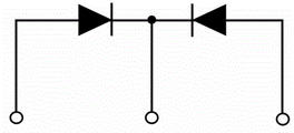
Diode is a kind of electronic device that can unidirectional conduction current, and this unilateral conduction of diode is normally used for the rectifying part of power source products.Fig. 1 is TO-220 encapsulation Schottky diode (Schottky Barrier Diode) schematic diagram; Schottky (Schottky) diode also claims Schottky barrier diode (being called for short SBD); it is a kind of low-power consumption, ultra-speed semiconductor device; be widely used in the circuit such as Switching Power Supply, frequency converter, driver; do high frequency, low pressure, large current commutates diode, fly-wheel diode, the use of protection diode, or in the circuit such as microwave communication, do rectifier diode, the use of small-signal detector diode.Shown in Fig. 2, being used in the problem existing in the diode rectifier circuit in Switching Power Supply has: 1, because heat dissipation problem causes Switching Power Supply localized hyperthermia; 2, electromagnetic interference; 3, the consistency of circuit is poor.
Summary of the invention
In view of the deficiency that prior art exists, the utility model, according to the circuit structure of Fig. 2, has proposed a kind of diode modules assembly for rectification circuit.
The technical scheme that the utility model taked is for achieving the above object: a kind of diode modules assembly for rectification circuit, is characterized in that: comprise fixed screw, insulation grain, metal shell, silica gel pad, the first conductive plate, the double diode group being formed by several double diodes, fixed head, the second conductive plate, the U.S. paper of promise, the 3rd conductive plate and printed circuit board (PCB), will be insulated by screw successively by fixed screw, metal shell, silica gel pad, conductive plate, double diode group and fixed head are locked together, be placed in again on the second conductive plate, the second conductive plate is placed on the 3rd conductive plate by the U.S. paper of promise, 1 pin of double diode group is welded on respectively on the second conductive plate terminal, 2 pin are welded on respectively on the first conductive plate terminal, 3 pin are welded on respectively on the 3rd conductive plate terminal, and are fixed on printed circuit board (PCB) the first conductive plate by the fixing ear on metal shell, the second conductive plate and the 3rd conductive plate are welded on printed circuit board (PCB) by pin, and metal shell inside is perfused with casting glue.
Feature of the present utility model and beneficial effect are: one group of double diode is made to an independently structure, and this structure adopts metal shell, can effectively reduce electromagnetic interference; The double diode group of metal shell inside is several double diode parallel-connection structures, and module splicing ear is drawn by conductive plate, has improved the rated current of assembly; Between conductive plate and metal shell, adopt heat conductive insulating silica gel pad effectively to isolate, guarantee good heat conductive effect; Be connected by screw, guaranteed the stability of module; Silicon gel embedding for inside configuration, has strengthened heat conduction and heat radiation effect, has guaranteed the temperature consistency of diode group.
Accompanying drawing explanation
Fig. 1 is double diode schematic diagram;
Fig. 2 is diode rectifier circuit schematic diagram;
Fig. 3 is the utility model exploded view;
Fig. 4 is the utility model embedding schematic diagram;
Fig. 5 is the utility model appearance figure;
Fig. 6 is the utility model printed circuit board (PCB) welding schematic diagram.
Embodiment
Below in conjunction with drawings and Examples, the utility model is described in further detail:
As Fig. 2, Fig. 3, Fig. 4, shown in Fig. 5 and Fig. 6, a kind of diode modules assembly for rectification circuit comprises fixed screw 1, insulation grain 2, metal shell 3, silica gel pad 4, the first conductive plate 5, double diode group 6, fixed head 7, the second conductive plate 8, the U.S. paper 9 of promise, the 3rd conductive plate 10 and printed circuit board (PCB) 11, will insulate 2 by fixed screw 1 successively by screw, metal shell 3, silica gel pad 4, conductive plate 5, double diode group 6 and fixed head 7 are locked together, be placed in again on the second conductive plate 8, the second conductive plate 8 is placed on the 3rd conductive plate 10 by the U.S. paper 9 of promise, 1 pin of double diode group 6 is welded on respectively on the second conductive plate 8 terminals, 2 pin are welded on respectively on the first conductive plate 5 terminals, 3 pin are welded on respectively on the 3rd conductive plate 10 terminals, and are fixed on printed circuit board (PCB) 11 the first conductive plate 5 by the fixing ear on metal shell 3, the pin of the second conductive plate 8 and the 3rd conductive plate 10 is welded on printed circuit board (PCB) 11, and metal shell 3 inside are perfused with casting glue 12.
Embodiment: accompanying drawing has provided the embodiment of a double diode group of 5 double diode compositions, but is not limited to this, should need to surely drink according to user.But at least should comprise two double diodes.What pour in whole metal shell inside is silicon gel, or adopts other casting glue that possesses thermal conductive resin, has some strength.Metal shell can adopt the metal material of any good conductive thermal conductive property.
This diode modules component application, in rectification circuit, has met the design requirement of rectification circuit.
Claims (1)
1. for a diode modules assembly for rectification circuit, it is characterized in that: comprise fixed screw (1), insulation grain (2), metal shell (3), silica gel pad (4), the first conductive plate (5), the double diode group (6) being formed by several double diodes, fixed head (7), the second conductive plate (8), the U.S. paper of promise (9), the 3rd conductive plate (10) and printed circuit board (PCB) (11), by fixed screw (1) by screw will insulate successively (2), metal shell (3), silica gel pad (4), conductive plate (5), double diode group (6) and fixed head (7) are locked together, be placed in again on the second conductive plate (8), the second conductive plate (8) is placed on the 3rd conductive plate (10) by the U.S. paper of promise (9), 1 pin of double diode group (6) is welded on respectively on the second conductive plate (8) terminal, 2 pin are welded on respectively on the first conductive plate (5) terminal, 3 pin are welded on respectively on the 3rd conductive plate (10) terminal, and it is upper to be fixed on printed circuit board (PCB) (11) by the fixing ear on metal shell (3), the first conductive plate (5), it is upper that the second conductive plate (8) and the 3rd conductive plate (10) are welded on pcb board (11) by pin, and metal shell (3) inside is perfused with casting glue (12).
Priority Applications (1)
| Application Number | Priority Date | Filing Date | Title |
|---|---|---|---|
| CN201320836850.6U CN203617293U (en) | 2013-12-18 | 2013-12-18 | Diode module assembly for rectifier circuit |
Applications Claiming Priority (1)
| Application Number | Priority Date | Filing Date | Title |
|---|---|---|---|
| CN201320836850.6U CN203617293U (en) | 2013-12-18 | 2013-12-18 | Diode module assembly for rectifier circuit |
Publications (1)
| Publication Number | Publication Date |
|---|---|
| CN203617293U true CN203617293U (en) | 2014-05-28 |
Family
ID=50769919
Family Applications (1)
| Application Number | Title | Priority Date | Filing Date |
|---|---|---|---|
| CN201320836850.6U Expired - Fee Related CN203617293U (en) | 2013-12-18 | 2013-12-18 | Diode module assembly for rectifier circuit |
Country Status (1)
| Country | Link |
|---|---|
| CN (1) | CN203617293U (en) |
Cited By (1)
| Publication number | Priority date | Publication date | Assignee | Title |
|---|---|---|---|---|
| US11511527B2 (en) | 2020-04-14 | 2022-11-29 | Saint-Gobain Performance Plastics Corporation | Composite film |
-
2013
- 2013-12-18 CN CN201320836850.6U patent/CN203617293U/en not_active Expired - Fee Related
Cited By (2)
| Publication number | Priority date | Publication date | Assignee | Title |
|---|---|---|---|---|
| US11511527B2 (en) | 2020-04-14 | 2022-11-29 | Saint-Gobain Performance Plastics Corporation | Composite film |
| US11813822B2 (en) | 2020-04-14 | 2023-11-14 | Saint-Gobain Performance Plastics Corporation | Composite film |
Similar Documents
| Publication | Publication Date | Title |
|---|---|---|
| CN102201449B (en) | Low-heat-resistance packaging structure of power MOS (Metal Oxide Semiconductor) device | |
| CN103794578A (en) | High-frequency large-power silicon carbide MOSFET module | |
| CN203746828U (en) | High-frequency large-power silicon-carbide MOSFET module | |
| CN203617293U (en) | Diode module assembly for rectifier circuit | |
| CN204793295U (en) | Slim power module | |
| CN102163928A (en) | Special ultrahigh-power rectification power electronic device module for ultrasonic welding machine | |
| CN204792757U (en) | Crimping formula power device packagiing of low thermal resistance | |
| CN209056480U (en) | A kind of ceramic copper-clad panel assembly applied to IGBT power module encapsulation | |
| CN203774281U (en) | Intelligent power module integrally injection-moulded and packaged | |
| CN104052244B (en) | Power module | |
| CN204991686U (en) | Power device heat abstractor of well high -voltage electrical equipment | |
| TWM506371U (en) | A whole structure of an intelligent power semiconductor module having an integrated heat sink | |
| CN207638569U (en) | A kind of three-phase commutation bridge | |
| CN203983160U (en) | A kind of solid-state relay with Rapid Thermal dissipation | |
| CN202259441U (en) | Novel LED chip | |
| CN209592027U (en) | A kind of two-sided cooling structure of SiC module | |
| CN205142648U (en) | Heat conduction base plate of device and device that generates heat generate heat | |
| CN204733087U (en) | A kind of high heat conduction and heat radiation rectifier bridge structure | |
| CN204858955U (en) | Igto packaging structure | |
| CN203536415U (en) | Thyristor module device | |
| CN218333755U (en) | High power density's little equipment chip power | |
| CN204204849U (en) | A kind of chip-packaging structure | |
| CN204216023U (en) | A kind of triode with radiating surface | |
| CN203644755U (en) | Large-power square-sheet silicon controlled rectifier encapsulation structure | |
| CN103646927B (en) | High-power square piece silicon controlled rectifier packaging structure |
Legal Events
| Date | Code | Title | Description |
|---|---|---|---|
| C14 | Grant of patent or utility model | ||
| GR01 | Patent grant | ||
| CF01 | Termination of patent right due to non-payment of annual fee |
Granted publication date: 20140528 Termination date: 20181218 |
|
| CF01 | Termination of patent right due to non-payment of annual fee |