CN1977344A - Compliant electrical contact assembly - Google Patents
Compliant electrical contact assembly Download PDFInfo
- Publication number
- CN1977344A CN1977344A CNA2005800133873A CN200580013387A CN1977344A CN 1977344 A CN1977344 A CN 1977344A CN A2005800133873 A CNA2005800133873 A CN A2005800133873A CN 200580013387 A CN200580013387 A CN 200580013387A CN 1977344 A CN1977344 A CN 1977344A
- Authority
- CN
- China
- Prior art keywords
- contactor
- coil
- hole
- electrical contact
- assembly
- Prior art date
- Legal status (The legal status is an assumption and is not a legal conclusion. Google has not performed a legal analysis and makes no representation as to the accuracy of the status listed.)
- Pending
Links
- 238000007906 compression Methods 0.000 claims abstract description 45
- 230000006835 compression Effects 0.000 claims abstract description 41
- 239000000463 material Substances 0.000 claims description 16
- 239000004020 conductor Substances 0.000 claims description 14
- 229920001971 elastomer Polymers 0.000 abstract description 13
- 239000000806 elastomer Substances 0.000 abstract description 6
- 239000011295 pitch Substances 0.000 abstract 1
- 239000000523 sample Substances 0.000 description 9
- 229910052751 metal Inorganic materials 0.000 description 8
- 239000002184 metal Substances 0.000 description 8
- 238000012360 testing method Methods 0.000 description 8
- 238000005452 bending Methods 0.000 description 7
- 238000005516 engineering process Methods 0.000 description 6
- 230000000694 effects Effects 0.000 description 4
- 229910010293 ceramic material Inorganic materials 0.000 description 3
- 239000011148 porous material Substances 0.000 description 3
- KDLHZDBZIXYQEI-UHFFFAOYSA-N Palladium Chemical compound [Pd] KDLHZDBZIXYQEI-UHFFFAOYSA-N 0.000 description 2
- XUIMIQQOPSSXEZ-UHFFFAOYSA-N Silicon Chemical compound [Si] XUIMIQQOPSSXEZ-UHFFFAOYSA-N 0.000 description 2
- 230000005611 electricity Effects 0.000 description 2
- 230000006698 induction Effects 0.000 description 2
- 238000005259 measurement Methods 0.000 description 2
- 230000003071 parasitic effect Effects 0.000 description 2
- BASFCYQUMIYNBI-UHFFFAOYSA-N platinum Chemical compound [Pt] BASFCYQUMIYNBI-UHFFFAOYSA-N 0.000 description 2
- 229910052710 silicon Inorganic materials 0.000 description 2
- 239000010703 silicon Substances 0.000 description 2
- 238000012546 transfer Methods 0.000 description 2
- 229910001369 Brass Inorganic materials 0.000 description 1
- 229910000906 Bronze Inorganic materials 0.000 description 1
- RYGMFSIKBFXOCR-UHFFFAOYSA-N Copper Chemical compound [Cu] RYGMFSIKBFXOCR-UHFFFAOYSA-N 0.000 description 1
- BQCADISMDOOEFD-UHFFFAOYSA-N Silver Chemical compound [Ag] BQCADISMDOOEFD-UHFFFAOYSA-N 0.000 description 1
- 229910000831 Steel Inorganic materials 0.000 description 1
- HCHKCACWOHOZIP-UHFFFAOYSA-N Zinc Chemical compound [Zn] HCHKCACWOHOZIP-UHFFFAOYSA-N 0.000 description 1
- 229910045601 alloy Inorganic materials 0.000 description 1
- 239000000956 alloy Substances 0.000 description 1
- -1 beallon Substances 0.000 description 1
- 239000010951 brass Substances 0.000 description 1
- 239000010974 bronze Substances 0.000 description 1
- 238000010276 construction Methods 0.000 description 1
- 229910052802 copper Inorganic materials 0.000 description 1
- 239000010949 copper Substances 0.000 description 1
- KUNSUQLRTQLHQQ-UHFFFAOYSA-N copper tin Chemical compound [Cu].[Sn] KUNSUQLRTQLHQQ-UHFFFAOYSA-N 0.000 description 1
- 230000007812 deficiency Effects 0.000 description 1
- 230000009977 dual effect Effects 0.000 description 1
- 239000003792 electrolyte Substances 0.000 description 1
- 238000005538 encapsulation Methods 0.000 description 1
- 239000004744 fabric Substances 0.000 description 1
- 230000002349 favourable effect Effects 0.000 description 1
- 238000009408 flooring Methods 0.000 description 1
- PCHJSUWPFVWCPO-UHFFFAOYSA-N gold Chemical compound [Au] PCHJSUWPFVWCPO-UHFFFAOYSA-N 0.000 description 1
- 229910052737 gold Inorganic materials 0.000 description 1
- 239000010931 gold Substances 0.000 description 1
- 239000011810 insulating material Substances 0.000 description 1
- 238000004519 manufacturing process Methods 0.000 description 1
- 229910001092 metal group alloy Inorganic materials 0.000 description 1
- 229910001120 nichrome Inorganic materials 0.000 description 1
- 239000000615 nonconductor Substances 0.000 description 1
- 229910052763 palladium Inorganic materials 0.000 description 1
- 230000024241 parasitism Effects 0.000 description 1
- 229910052697 platinum Inorganic materials 0.000 description 1
- 238000012545 processing Methods 0.000 description 1
- 238000000926 separation method Methods 0.000 description 1
- 229920002379 silicone rubber Polymers 0.000 description 1
- 229910052709 silver Inorganic materials 0.000 description 1
- 239000004332 silver Substances 0.000 description 1
- 239000010935 stainless steel Substances 0.000 description 1
- 229910001220 stainless steel Inorganic materials 0.000 description 1
- 239000010959 steel Substances 0.000 description 1
- 238000013519 translation Methods 0.000 description 1
- 238000003466 welding Methods 0.000 description 1
- 210000002268 wool Anatomy 0.000 description 1
- 229910052725 zinc Inorganic materials 0.000 description 1
- 239000011701 zinc Substances 0.000 description 1
Images


Classifications
-
- H—ELECTRICITY
- H01—ELECTRIC ELEMENTS
- H01R—ELECTRICALLY-CONDUCTIVE CONNECTIONS; STRUCTURAL ASSOCIATIONS OF A PLURALITY OF MUTUALLY-INSULATED ELECTRICAL CONNECTING ELEMENTS; COUPLING DEVICES; CURRENT COLLECTORS
- H01R13/00—Details of coupling devices of the kinds covered by groups H01R12/70 or H01R24/00 - H01R33/00
- H01R13/02—Contact members
- H01R13/22—Contacts for co-operating by abutting
- H01R13/24—Contacts for co-operating by abutting resilient; resiliently-mounted
- H01R13/2407—Contacts for co-operating by abutting resilient; resiliently-mounted characterized by the resilient means
- H01R13/2421—Contacts for co-operating by abutting resilient; resiliently-mounted characterized by the resilient means using coil springs
-
- G—PHYSICS
- G01—MEASURING; TESTING
- G01R—MEASURING ELECTRIC VARIABLES; MEASURING MAGNETIC VARIABLES
- G01R1/00—Details of instruments or arrangements of the types included in groups G01R5/00 - G01R13/00 and G01R31/00
- G01R1/02—General constructional details
- G01R1/06—Measuring leads; Measuring probes
- G01R1/067—Measuring probes
- G01R1/06711—Probe needles; Cantilever beams; "Bump" contacts; Replaceable probe pins
- G01R1/06716—Elastic
-
- G—PHYSICS
- G01—MEASURING; TESTING
- G01R—MEASURING ELECTRIC VARIABLES; MEASURING MAGNETIC VARIABLES
- G01R1/00—Details of instruments or arrangements of the types included in groups G01R5/00 - G01R13/00 and G01R31/00
- G01R1/02—General constructional details
- G01R1/06—Measuring leads; Measuring probes
- G01R1/067—Measuring probes
- G01R1/06711—Probe needles; Cantilever beams; "Bump" contacts; Replaceable probe pins
- G01R1/06733—Geometry aspects
-
- H—ELECTRICITY
- H05—ELECTRIC TECHNIQUES NOT OTHERWISE PROVIDED FOR
- H05K—PRINTED CIRCUITS; CASINGS OR CONSTRUCTIONAL DETAILS OF ELECTRIC APPARATUS; MANUFACTURE OF ASSEMBLAGES OF ELECTRICAL COMPONENTS
- H05K7/00—Constructional details common to different types of electric apparatus
- H05K7/02—Arrangements of circuit components or wiring on supporting structure
- H05K7/10—Plug-in assemblages of components, e.g. IC sockets
- H05K7/1053—Plug-in assemblages of components, e.g. IC sockets having interior leads
- H05K7/1061—Plug-in assemblages of components, e.g. IC sockets having interior leads co-operating by abutting
- H05K7/1069—Plug-in assemblages of components, e.g. IC sockets having interior leads co-operating by abutting with spring contact pieces
-
- H—ELECTRICITY
- H01—ELECTRIC ELEMENTS
- H01R—ELECTRICALLY-CONDUCTIVE CONNECTIONS; STRUCTURAL ASSOCIATIONS OF A PLURALITY OF MUTUALLY-INSULATED ELECTRICAL CONNECTING ELEMENTS; COUPLING DEVICES; CURRENT COLLECTORS
- H01R12/00—Structural associations of a plurality of mutually-insulated electrical connecting elements, specially adapted for printed circuits, e.g. printed circuit boards [PCB], flat or ribbon cables, or like generally planar structures, e.g. terminal strips, terminal blocks; Coupling devices specially adapted for printed circuits, flat or ribbon cables, or like generally planar structures; Terminals specially adapted for contact with, or insertion into, printed circuits, flat or ribbon cables, or like generally planar structures
- H01R12/50—Fixed connections
- H01R12/51—Fixed connections for rigid printed circuits or like structures
- H01R12/52—Fixed connections for rigid printed circuits or like structures connecting to other rigid printed circuits or like structures
-
- H—ELECTRICITY
- H01—ELECTRIC ELEMENTS
- H01R—ELECTRICALLY-CONDUCTIVE CONNECTIONS; STRUCTURAL ASSOCIATIONS OF A PLURALITY OF MUTUALLY-INSULATED ELECTRICAL CONNECTING ELEMENTS; COUPLING DEVICES; CURRENT COLLECTORS
- H01R2201/00—Connectors or connections adapted for particular applications
- H01R2201/20—Connectors or connections adapted for particular applications for testing or measuring purposes
Landscapes
- Physics & Mathematics (AREA)
- General Physics & Mathematics (AREA)
- Engineering & Computer Science (AREA)
- Microelectronics & Electronic Packaging (AREA)
- Geometry (AREA)
- Measuring Leads Or Probes (AREA)
- Testing Of Individual Semiconductor Devices (AREA)
- Connecting Device With Holders (AREA)
- Manufacturing Of Electrical Connectors (AREA)
- Coupling Device And Connection With Printed Circuit (AREA)
Abstract
A compliant electrical contact assembly (11) for temporarily interfacing two electrical devices. The assembly (11) includes a contact (10) having loops (14) with axes forming with a closed coil with opposed contact points (16, 18). The axes is angled from the direction (17) of the compression force (15) holding the assembly (11) sandwiched between the electrical devices. The electrically shorted loops (14) of the coil slide on the surfaces of one another as the compression force (15) is applied, providing compliance. The contact (16, 18) can be made extremely small such that pitches in the micrometer range can be achieved with very low inductance values. The contact (10) is installed in a through aperture (24) in a dielectric panel (26) such that the contact points (16, 18)extend from opposed openings of the aperture (24). Optionally, the aperture (24) is filled with a compliant, conductive elastomer (36).
Description
Technical field
The present invention relates to electric contactor, relate in particular to the very little compliant electrical contact that has very low inductance at high frequency.
Background technology
The purposes of electric contactor is to provide separable electrical interconnected between two electric conductors.It is not to adopt such as welding or permanent mechanical system such as bonding but interim mechanical system is interconnected that separable feature means conductor.Therefore, in order to keep the favorable mechanical contact, used the form of certain spring force that two conductors are forced together so that harmful electrical effect of contactor drops to minimum.These electric contactors are called as compliance (elasticity) contactor.
Little compliance contactor is that integrated circuit (IC) is interconnected to the desirable any electric equipment of user separably is necessary.Main example is that IC is connected to test fixture and sorting unit, and these devices are used for testing in the mill and sorting IC.The compliance contactor is should be as much as possible minimum will arrive such as ghost effects such as inductance near electricity transparent (electricallytransparent), thereby these ghost effect meetings change and transfer to IC and reach the result that the signal from IC may lead to errors.
Another advantage that the compliance contactor provides is that they can compensate the non-coplanarity of the electronics of connection at measurement unit (UUT).Conducting spots inaccuracy coplane on the UUT, promptly they are not in same plane, even between the identical conducting spots of different UUT.The amount that the compliance contactor is different according to the physical location deflection of conducting spots.
The conventional compliance contactor that is used to be connected to UUT comprises: the spring probe, and conductive rubber, the compliant beam contactor, and the quilt that is called fuzz buttons is tied into a branch of metal wire.Every technology has been all for the non-coplanarity that overcomes between contact point provides required device, and provides uniformly by a plurality of contactors and to electrically contact.Every technology all has deficiency on a characteristic or another characteristic, and high electric parasitic character is all arranged.In addition, their manufacturing expenses are all more expensive relatively.
Typical spring probe comprises at least three or four parts, has sleeve pipe and one or two plunger of spring.Spring is accommodated in the sleeve pipe, and at the two ends of spring, the end of plunger is limited in two opposing open end of sleeve pipe.Spring is the plunger outward bias voltage, thereby provides spring force to the top of plunger.The spring probe can provide the compliance and the contact force of a great difference degree, and can contact very reliably repeatedly usually or a plurality of circulation.The spring probe can adapt to such as many different conduction interfaces such as pad, post, balls.Yet spring probe has dimensional problem, and promptly spring itself can not be accomplished very for a short time, otherwise can not keep in touch the stable spring force of device and contactor.Therefore, the spring probe is relatively large, causes producing when being used for the signal of telecommunication of higher frequency unacceptable big inductance.In addition, owing to must make respectively three elements earlier, and then they are assembled, so spring probe cost is higher relatively
The conductive rubber contactor is made up of dissimilar rubber and silicon with embedded conductive metal element.These contactor schemes have littler inductance than the spring probe usually, but compare with the spring probe, and its compliance is less and duty cycle that can use is also less.Thereby be lifted away from UUT at conducting spots and need add the 3rd conducting element to play the time spent of doing of stretching out member, use conductive rubber from the extended part of UUT or to system.Unit the 3rd has reduced the contact area of given contact pressure, thereby thereby the pressure that has increased unit are can obtain stable contact.Three element can be the button of the screw machine processing on the rubber that places between conducting spots.This three element only can add inductance to contact system.
The compliant beam contactor is made by electric conducting material, and this contactor forms at its end of linking the UUT conducting spots and obtains skew and contact pressure and the other end remains fixed to another conductor.In other words, pressure is provided by one or more conduction leaf springs.These contactors alter a great deal in shape and application.Some compliant beam contactor is enough little, can be effectively used to IC.Some compliant beam contactor uses such as other compliance materials such as rubber increases compliance or contact pressure to give the bar contact point.These types of back are littler than traditional compliant beam contactor, thereby littler inductance is arranged, and are more suitable for being used for the device of sorting higher frequency.Yet these contactors still show excessive slightly for the use in some radio frequency (RF) is used.
Fuzz buttons is relatively old but simple technology, and wherein metal wire is twisted and warped into cylindrical.Resultant shape seems to be very similar to the small column of being made up of steel wool.When cylinder was placed in the hole in a slice non-conducting material, it played the effect of the spring that is similar to the continuous electric short circuit.It provides inductance lower power path than other contactor technology.Be similar to the rubber contactor, fuzz buttons adopts three element usually, thereby generates and the contacting of fuzz buttons, and this three element need reach within the non-conductive hole.This three element has increased stray inductance, has reduced to transfer to UUT and from the signal of UUT.
The IC encapsulation technology just develops toward littler, higher frequency (faster) and more cheap direction, thereby causes that the electric contactor of these types has been had new requirement.They need carry out these requirements fully with minimum cost.
Summary of the invention
An object of the present invention is to provide a kind of assembly that comprises the compliance contactor, described compliance contactor has the self-induction lower than prior art in higher frequency.
Another object of the present invention provide can provide enough compliance to test the low self-induction contact assembly of various UUT.
Thereby the another purpose of this aspect provide can make the minimum low self-induction contactor assembly that is used for the test of conducting spots closely UUT.
Another object of the present invention provides the cheap relatively low self-induction contact assembly of cost.
The present invention is the assembly that temporary interface is provided between two electric devices.This assembly is sandwiched between two electric devices, and a compression stress keeps together this combination.This assembly comprises that self-induction is very low, the contactor of compliance.This contactor comprises having a pair of coil relative, that be used for being connected to the contact point of the conducting spots on the electric device.This coil and compression direction are at an angle.Angle is more little, and it is just big more to compress the required pressure of contactor.In compression process, when all coil loop edge slided over each other, they were electrical shorts.Coil only needs to cause short circuit when being enough to be compressed once encircling between adjacent wires, minimum can be just above 360 °.
Material can be any electric conducting material with intrinsic elastic characteristic, the shape of cross section of material can be an Any shape, comprise circle, square, triangle, ellipse, rectangle, perhaps star, the size of cross section does not need along length of material yet must be consistent.
Each all can be configured to a kind of in the various structures contact point.
Contactor is placed in the through hole in the electrolyte panel.All there is opening in the hole at the two ends of core.Contactor can be by the pin lock-bit that extends through the contactor coil center in the hole.Perhaps, the remaining space conductive elastomer filling that can increase elasticity and help to make the compliance of coil loop electrical short in the hole.
With reference to the accompanying drawings with detailed description of the present invention, other purpose of the present invention will be obvious.
Description of drawings
With reference to accompanying drawing so that essence of the present invention and purpose are more fully understood, wherein:
Fig. 1 is the stereogram with basic contactor of the present invention of concentric conductor;
Fig. 2 is the end view with contactor of vesica piscis;
Fig. 3 is the end view with contactor of parallel ring axis;
Fig. 4 is the cross-sectional view of assembly of the present invention and UUT and testboard;
Fig. 5 is the end view of contactor that has the gap of variation between the ring;
Fig. 6 is the stereogram with contactor of minimal coil;
Fig. 7 is the end view of the contactor made by the rectangular cross-sectional flooring;
Fig. 8 A-8E is the partial cross-section diagrammatic sketch that has the contactor of central straight lead in assembly;
Fig. 9 A and 9B are the front view and the end views of partial cross-section of contactor that has the straight lead of skew in assembly;
Figure 10 A and 10B are the front view and the end views of partial cross-section of contactor that has the straight lead of inclination in assembly;
Figure 11 A and 11B are the front view and the end views of partial cross-section that has the contactor of hook lead in assembly;
Figure 12 A and 12B are front view and the end views with hook lead and partial cross-section of the contactor of tangential lead.
Figure 12 C and 12D are the overlooking and face upwarding stereogram of cover of Figure 12 A and 12B;
Figure 13 A and 13B are front view and the end views with contactor of tubercle (nub) contact point;
Figure 14 A and 14B are front view and the end views that has with the contactor of another tubercle contact point of tangential wire form;
Figure 15 A and 15B are front view and the end views with contactor of annular contact point;
Figure 16-the 21st, the end view of the cross section of various contactor capturing structures;
Figure 22 is the upward view of the cross section of contactor capturing structure;
Figure 23 is the stereogram of the contactor that circularizes of lead; And
Figure 24 is the stereogram that lead is tapered to contactor a little.
Embodiment
The present invention is between two electric devices, provide the assembly 11 of interface usually between measurement unit (UUT) 2 and testboard 4.Assembly 11 comprises the compliant electrical contact 10 with very low self-induction.
Reach as mentioned above shown in Fig. 4, contactor provides interim and has been electrically connected between the conducting spots 6,8 of UTT2 and testboard 4.For good electrical connection is provided, compress contactor 10 by between UUT2 and testboard 4, applying, thereby make the spring force of contactor 10 that the contact point 16,18 of contactor 10 is shifted onto on UUT conducting spots 6 and the testboard conducting spots 8 along the compression stress 15 of compression direction 17.
In case gap 44 is closed, when ring 14 slides over each other on its edge, in the residual compression process of whole contact 10, be electrical short.12 needs of coil cause short circuit once encircling when enough being compressed between contact point 16,18, therefore can lack very much and have low-down electricity parasitism.Minimum coil has only more more slightly than a ring, as shown in Figure 6.Material is minimum just to be surpassed 360 ° by coiling, thereby makes the end of coil 12 contact in compression.
The size of angle 19 depends on concrete application and the required compliance forces of this application.Angle 19 is more little, and the required power of compression contactor 10 is big more, means that promptly contactor 10 will provide bigger power to conducting spots 6,8.The size of angle 19 has the limit.When angle 19 near zero the time, when being parallel to compression direction 17, in case coil is in contact with one another, contactor 10 can not further compress again.And when angle 19 surpasses 90 °, when surpassing the direction perpendicular to compression direction 17, coil 12 unlikely being in contact with one another between contact point, to form short circuit.Therefore, the actual range of angle 19 is from about 5 ° to about 90 °.
Except angle of inclination 19, the power of contactor 10 is also determined by other coil parameter such as the volume of materials used in making contactor the curve of side-play amount, for example, the number of wire cross-sectional dimension, coil diameter and ring, and shape of cross section and material.The shape of cross section of material can be a circle as shown in fig. 1, or other shape, comprises as shown in Figure 7 square, triangle, ellipse, rectangle or star.The present invention also conceives cross sectional dimensions needn't be along the length unanimity of material.When use had the cross sectional material of flattened side such as rectangle or star etc., than using circle or oval cross section, adjacent ring can be along more high surface area contact.Therefore, constitute the shortest possible power path, thereby caused the lower connection of inductance.Yet owing to cost and other reason, the material with flattened side is not necessarily more excellent with respect to circle or oval material.
Material can be made up of any electric conducting material with intrinsic elastic characteristic, and for example, stainless steel, beallon, copper, brass, nichrome, and palladium-rare metal alloy are such as PALINEY
, 35% palladium, 30% silver medal, 14% bronze medal, 10% gold medal, 10% platinum, and the alloy of 1% zinc.All these materials all can be used for from malleableize to the different hardness that hardens fully.
As mentioned above, contactor 10 is used in to the conducting spots between two electric devices 6,8 provides in the assembly 11 of interim electrical connection.Usually, shown in Fig. 8 A and 8B, contactor 10 is placed in the through hole 24 in the dielectric panel 26.All there is opening 28 in hole 24 at the two ends of section 30, and contact point 16,18 stretches out by these two openings.
When along compression direction 17 when the contact point 16,18 of the opening 28 that stretches out dielectric panel 26 applies compression stress 15, as shown in Fig. 8 A, the compression of ring 14 left side and the right side expansion of ring increase the diameter of coil 12 usually.When applying compression stress 15, the position of device 10 is kept in touch in hole 24.Hole 24 also can be disperseed to keep in touch the complete of device 10 by preventing coil loop 14 under pressure.
By adopting minimum metal wire and in dielectric panel 26, forming hole 24, can do contactor 10 minimum, be used to test pitch less than 0.5 millimeter UUT.Contactor 10 is applicable to that pitch pops one's head at millimetre-sized silicon wafer.
Fig. 8 A-22 shows a plurality of different contact points, hole, dielectric panel and contactor lock-bit example of structure.It should be noted that two contact point 1618 structures among every width of cloth figure are identical.The present invention does not require two contact points 16,18th of single contactor, and is same, but conceive two contact points 16,18 different structures can be arranged.Shown in structure only make example rather than the present invention be defined in any specific contact point, hole or dielectric panel configuration.Any contact point, hole and/or the panel construction of serving application-specific are conceived by the present invention.
In Fig. 8 A-8E, contact point 16 is in the end of central straight lead.The center that is usually located at coil 12 is seen such as common and compression direction 17 lead 72 in line of being bent to form of 74 places by three dimensions in the end of coil 12 from contact point 16.The cross sectional dimensions of the centre portion 30 in hole 24 is bigger slightly than the full-size of the contactor 10 vertical with lead 72.In the structure of Fig. 8 C, centre portion 30 has oval cross section, has large-size at the dimension 40 of coil 12.Because coil 12 is not in dimension 42 expansions, so less dimension 42 can be the same with coil dimension.Because lead 72 is positioned at the center in hole 24, so opening 28 common and centre portion 30 coaxial lines.The axially bored line 58 of Fig. 8 A and compression direction 17 are in line.Opening 28 less than coil 12 so that contactor 10 by hole 24 lock-bits.
The dielectric panel 26 of Fig. 8 A has the bottom thin plate 34 that comprises an opening 28 and most of centre portion, and the top lip 32 that comprises top centre portion and another opening 28.Contactor 10 is placed on the bottom sheet section in hole 24, and thin plate 32,34 is sandwiched in together so that contactor 10 locks are positioned at hole 24.
The replacement that contactor 10 in the dielectric panel 26 has been shown among Fig. 8 D is arranged.It should be noted that a contact point 16 extends fartherly than another contact point 18 from coil 12, and hole 24 prolongs and staggers.Adopt this layout, contactor 10 can be placed tightlyer together.The application-specific of this layout comprises 4 metal wires tests, and wherein every IC lead needs two contact points, and one is used for drive current and another is used for the high impedance induction.
Another replacement that contactor 10 in the dielectric panel 26 has been shown among Fig. 8 E is arranged.Thereby axially bored line 58, inclination make lead 72 mutually in line, but misaligned with compression direction 17.This arranges the translation that allows between contact point 16 and the electrical device conduction point 6.Panel 26 is divided to split so that two parts in hole 24 depart from each other.
In the structure of Fig. 9 A and 9B, contact point 16 is positioned at and compression direction 17 also in line the end of offset straight leads 76.It is with the different of central straight lead 72, and the end of coil 12 is in the tangential extension of ring 14, then only two dimension bendings, rather than at the center by being bent to form of three dimensions, so lead 76 is positioned at a side of coil 12.Since the center that lead 76 departs from contactor 10, opening 28 and central section 30 disalignments, but in the one side.
Fig. 9 A shows the advantage of parallel wire 76: contactor 10 can be arranged very closely together and not need the concentric conductor 72 among the image pattern 8D to prolong arbitrary lead 76 like that.Be similar to the layout among Fig. 8 D, the application-specific of this layout comprises 4 metal wires tests, and wherein every IC lead needs two contact points, and one is used for drive current and another is used for the high impedance induction.
The dielectric panel 26 of Fig. 9 has two mirror image thin plates 46,48, and wherein every thin plate contains an opening 28 and half centre portion 30.Contactor 10 is placed on a side in hole 24, thin plate 46,48 be sandwiched in together with contactor 10 lock-bits in hole 24.
In the structure of Figure 10 A and 10B, contact point 16 is positioned at the end of the straight lead 78 that tilts, and this straight lead forms so that lead 78 extends on ring 14 tangential by stopping ring 14.It is misaligned that the result is exactly this lead and compression direction 17, shown in Figure 10 B.Because lead 78 is tangent with coil 12, so it is perpendicular to coil axis 38.Be similar to the hole opening of those offset straight leads, hole opening 28 is positioned at a side of centre portion 30.Yet,, can prolong opening 28 to allow motion perpendicular to compression direction 17 because the straight lead 78 that tilts favours compression direction 17.
Perhaps, as shown in Figure 10 A and 10B, the residual gap after contactor 10 is installed in the hole 24 can use compliance, conductive elastomer 36 to fill.Elastomer 36 serves a dual purpose.It has increased the elasticity of contactor 10, means that contactor 10 can bear the more work cycle when not having elastomer 36.Elastomer 36 also helps coil loop 14 electrical shorts, thereby makes the electric parasitic value of contact system drop to minimum potentially.
In the structure of Figure 11 A and 11B, contact point 16 is sides 82 of hook lead 80.Be similar to offset straight lead 76, tangentially extend from coil 12 end of coil 12, is bent to hook 84 then, so that contact point 16 is along the side 82 of lead 80 rather than in the end 86 of lead 80.Hook 84 can provide the Any shape of required function.The hook 84 of Figure 11 A is made of two bendings 88 and straight line portion 90 between the two.Perhaps, hook 84 can be the single bending greater than 90 °.Hole opening 28 is grooves that centre portion 30 is divided equally, thereby makes hook 84 can bend in the groove when being compressed.
In the structure of Figure 12 A and 12B, the upper surface 102 that contact point 16 is hooks 100.The end of coil 12 is bent to hook 100, so that contact point 16 is along the side 102 of hook 100 rather than the end of lead then from coil 12 tangential extensions and angled with compression direction 17.The hook 100 of Figure 12 is made of about 90 ° single bending.Another contact point 18 is ends of lead 104, and this lead and coil 12 general tangential and angled with compression direction 17 are shown in Figure 12 A.Lead 104 can with mode like Figure 10 category-B and coil in line, perhaps be bent to more near with compression direction 17 in line, as Fig. 8 and 12B.
In the structure of Figure 13 A and 13B, contact point 16 is tubercles 92, promptly except encircling 14 bending without any the end of the coil 12 of bending.Tubercle 92 and compression direction 17 are in line.Perhaps, shown in Figure 14 A and 14B, tubercle 92 is positioned at the end with the tangent very short lead 94 of coil 12, it can with compression direction 17 in line can be not yet with its in line.
In the structure of Figure 15 A and 15B, contact point 16 is sides 96 of ring 14.It is with Figure 13 A and 13B in tubercle 92 essentially identical designs, different just rotated coil 12 so that will encircle 14 side 96 rather than the end 98 of coil 12 as contact point 16.If two contact points 16,18 then must have 1.5 rings 14 at least all in the side of ring 14.
Because the contact structure of Figure 13 A-15B is not similar to the lead that extends coil 14 substantially of other contact structure, the pore structure with centre portion and littler opening differs optimum performance is provided surely.Figure 16-22 shows the pore structure that is more suitable in these contact structures.Can use these pore structures that adopts the structure outside the opening of narrow hole to come lockout contactor 10, it is suitable for all contact structures.
The hole 24 of Figure 16 has and compression direction 17 axis 58 in line, and wherein contactor 10 is placed on centre portion 30, and contact point 16,18 extends opening 28.Contactor 10 is maintained at the appropriate location, and ceramic material 52 solidifies so that contactor 10 is fixed on correct direction.Ceramic material 52 can be conductor or non-conductor.The hole 24 of Figure 17 has from the axis 58 of compression direction 17 inclinations, and wherein the inclination angle is basically perpendicular to the angle of coil axis 38.Contactor 10 is not by frictional fit, is that hole 24 is slightly less than contactor 10, is secured in centre portion by the ceramic material that is similar to Figure 16 exactly.Contact point 16,18 extends opening 28.
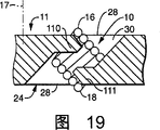
Figure 18-22 shows the whole bag of tricks of lock-bit contactor, and the pin of some of them form extends through the center of coil 12.
The hole 24 of Figure 18 tilts from compression direction 17, and wherein hang down substantially as for the angle of coil axis 38 in the inclination angle.The pin of fixed contact 10 is the rods 54 that extend through hole 56 and coil 12 centers in the dielectric panel 26. Contact point 16,18 extends opening 28.
In Figure 19, pin is the projection 110 of extending the wall of 24 the centre portion 30 of portalling, and hole 24 favours compression direction 17.Projection 110 extends into coil 12 so that contactor 10 is fixed in the hole 24.Second projection 111 is selectable.In Figure 20, pin is a pair of coaxial protrusions 112 of extending the wall of 24 the centre portion 30 of portalling, and hole 24 favours compression direction 17.Interface 116 place's horizontal separation that dielectric panel 26 is being divided hole 24 equally.Contactor 10 is installed in a side in hole 24, and so latter two panel component 118,120 is fitted together so that two projectioies can both extend into contactor 10 by horizontal group.
The pin of Figure 21 also is the projection 122 of extending the wall of centre portion 30.After installing contactor 10, connector 126 is installed in the hole 24 so that contactor 10 is fixed in the hole.Alternatively, projection 124 can be arranged on connector 126.
In Figure 22, contactor 10 is placed in the hole 24.It is the elastic webbing 60 that extends through the center of hole 62 in the dielectric panel and coil 12 that contactor 10 is fixed on pin in the hole 24.Be with 60 can extend through more than one contactor 10.Owing to be with 60 to be flexible, contactor 10 needn't be arranged in and make all holes 62 in a straight line, but can be around the turning bending.Be with 60 by forming such as insulating material such as silicon rubber.
Thus, illustrated and described a kind of compliant electrical contact assembly that satisfies above-mentioned target.
Owing to can in present disclosure, carry out some change and can not deviate from scope of the present invention, be intended to in above specification, describe and in the accompanying drawings shown in all themes be interpreted as illustrative rather than restrictive, sense.
Claims (8)
1. one kind is applicable between the conducting spots of the conducting spots of first electric device and second electric device interim compliant electrical contact assembly that is electrically connected is provided, described a plurality of electric device is by making them be compressed in the described assembly between them in the compression stress on the compression direction, described assembly comprises:
(a) at least one compliant electrical contact, described contactor comprises one section intrinsic flexible electric conducting material, described material is shaped as the coil with the number of rings that is slightly more than a ring at least, and each ring all has an axis, and described a plurality of ring axis become first angle with described pressure direction; Described contactor has and is used for the roughly relative contact point that is electrically connected with described conducting spots, and in the described contact point one roughly tangent with described coil and become on the lead of second angle with described compression direction, and another described contact point is on hook lead; And
(b) each contactor in described at least one electric contactor there is the dielectric panel of a through hole, in described hole, makes described contact point extend the relative opening that passes described hole thereby described contactor is of the lock bit.
2. compliant electrical contact assembly as claimed in claim 1 is characterized in that described ring axis is coaxial.
3. compliant electrical contact assembly as claimed in claim 1 is characterized in that, described first angle is in from about 5 degree to the scope of about 90 degree.
4. compliant electrical contact assembly as claimed in claim 1, it is characterized in that, first opening in the described relative opening be with described hole be that holistic groove and described hook lead extend through this groove, and in the cover in being matched with an openend in described hole, relative with described groove of second opening in the described relative opening.
5. compliant electrical contact assembly as claimed in claim 1 is characterized in that described cover is press fit in the described openend.
6. one kind is applicable between the conducting spots of the conducting spots of first electric device and second electric device interim compliant electrical contact assembly that is electrically connected is provided, described a plurality of electric device is by making them be compressed in the described assembly between them in the compression stress on the compression direction, described assembly comprises:
(a) at least one compliant electrical contact, described contactor comprises one section intrinsic flexible electric conducting material, described material is shaped as the coil with the number of rings that is slightly more than a ring at least, and each ring all has an axis, and described a plurality of ring axis and described pressure direction are angled; Described contactor has the roughly relative contact point that is used for described conducting spots electrical connection; And
(b) each contactor in described at least one electric contactor is all had a dielectric panel that has a through hole of axis, described contactor be extended pass described coil the pin lock-bit in described hole.
7. compliant electrical contact assembly as claimed in claim 6 is characterized in that described ring axis is coaxial.
8. compliant electrical contact assembly as claimed in claim 6 is characterized in that, described angle is in from about 5 degree to the scope of about 90 degree.
Applications Claiming Priority (2)
| Application Number | Priority Date | Filing Date | Title |
|---|---|---|---|
| US10/834,727 | 2004-04-29 | ||
| US10/834,727 US6909056B2 (en) | 2002-01-17 | 2004-04-29 | Compliant electrical contact assembly |
Publications (1)
| Publication Number | Publication Date |
|---|---|
| CN1977344A true CN1977344A (en) | 2007-06-06 |
Family
ID=35320456
Family Applications (1)
| Application Number | Title | Priority Date | Filing Date |
|---|---|---|---|
| CNA2005800133873A Pending CN1977344A (en) | 2004-04-29 | 2005-04-28 | Compliant electrical contact assembly |
Country Status (9)
| Country | Link |
|---|---|
| US (1) | US6909056B2 (en) |
| EP (1) | EP1741111A4 (en) |
| JP (1) | JP2007535795A (en) |
| KR (1) | KR20070007934A (en) |
| CN (1) | CN1977344A (en) |
| CA (1) | CA2564191A1 (en) |
| IL (1) | IL178355A0 (en) |
| SG (1) | SG136963A1 (en) |
| WO (1) | WO2005109450A1 (en) |
Families Citing this family (16)
| Publication number | Priority date | Publication date | Assignee | Title |
|---|---|---|---|---|
| US7140884B2 (en) * | 2005-01-26 | 2006-11-28 | International Business Machines Corporation | Contact assembly and method of making thereof |
| TWI261672B (en) * | 2005-03-15 | 2006-09-11 | Mjc Probe Inc | Elastic micro probe and method of making same |
| US7402051B1 (en) * | 2005-11-10 | 2008-07-22 | Antares Advanced Test Technologies, Inc. | Interconnect assembly for testing integrated circuit packages |
| TWI332086B (en) * | 2006-10-24 | 2010-10-21 | Ind Tech Res Inst | Multi-layer electric probe and fabricating method |
| US7520753B1 (en) | 2008-03-31 | 2009-04-21 | International Business Machines Corporation | Method of using coil contact as electrical interconnect |
| JP5686009B2 (en) * | 2011-03-18 | 2015-03-18 | 富士通株式会社 | Substrate unit and method for manufacturing substrate unit |
| DE202011005271U1 (en) * | 2011-04-14 | 2011-07-26 | Rosenberger Hochfrequenztechnik Gmbh & Co. Kg | Connector with a contact element |
| JP5718203B2 (en) * | 2011-10-05 | 2015-05-13 | 富士通コンポーネント株式会社 | Socket module and socket |
| USRE47459E1 (en) | 2011-10-24 | 2019-06-25 | Ardent Concepts, Inc. | Controlled-impedance cable termination using compliant interconnect elements |
| USRE46958E1 (en) | 2011-10-24 | 2018-07-17 | Ardent Concepts, Inc. | Controlled-impedance cable termination using compliant interconnect elements |
| EP3413407B1 (en) * | 2011-10-24 | 2023-06-07 | Ardent Concepts Inc. | Controlled-impedance cable termination using compliant interconnect elements |
| US8764458B1 (en) * | 2012-09-10 | 2014-07-01 | Amazon Technologies, Inc. | Spring connector and corresponding guide element |
| EP3216091A4 (en) * | 2014-11-06 | 2018-07-11 | Ardent Concepts Inc. | Controlled-impedance cable termination using compliant interconnect elements |
| US10931040B1 (en) * | 2018-08-02 | 2021-02-23 | Ardent Concepts, Inc. | Controlled-impedance circuit board connector assembly |
| KR102153299B1 (en) * | 2019-05-31 | 2020-09-21 | 주식회사 이노글로벌 | By-directional electrically conductive pin, by-directional electrically conductive module and manufacturing method thereof |
| WO2021261285A1 (en) * | 2020-06-22 | 2021-12-30 | 株式会社ヨコオ | Inspection device |
Family Cites Families (21)
| Publication number | Priority date | Publication date | Assignee | Title |
|---|---|---|---|---|
| US4029375A (en) | 1976-06-14 | 1977-06-14 | Electronic Engineering Company Of California | Miniature electrical connector |
| EP0385142B1 (en) | 1989-02-28 | 1995-09-27 | Fujitsu Limited | Electrical connecting apparatus |
| US4998886A (en) | 1989-07-07 | 1991-03-12 | Teledyne Kinetics | High density stacking connector |
| EP0462706A1 (en) | 1990-06-11 | 1991-12-27 | ITT INDUSTRIES, INC. (a Delaware corporation) | Contact assembly |
| CA2095119C (en) | 1990-10-29 | 2002-06-04 | Welles K. Reymond | Electrical connectors having tapered spring contact element |
| US5101553A (en) | 1991-04-29 | 1992-04-07 | Microelectronics And Computer Technology Corporation | Method of making a metal-on-elastomer pressure contact connector |
| US5167512A (en) * | 1991-07-05 | 1992-12-01 | Walkup William B | Multi-chip module connector element and system |
| US5230632A (en) | 1991-12-19 | 1993-07-27 | International Business Machines Corporation | Dual element electrical contact and connector assembly utilizing same |
| GB2273830B (en) | 1992-12-24 | 1997-04-16 | Whitaker Corp | Electrical contact elements for interposer structures |
| EP0616394A1 (en) | 1993-03-16 | 1994-09-21 | Hewlett-Packard Company | Method and system for producing electrically interconnected circuits |
| US5495667A (en) | 1994-11-07 | 1996-03-05 | Micron Technology, Inc. | Method for forming contact pins for semiconductor dice and interconnects |
| US5667410A (en) | 1995-11-21 | 1997-09-16 | Everett Charles Technologies, Inc. | One-piece compliant probe |
| DE19781697B4 (en) * | 1996-04-12 | 2010-04-22 | NHK Spring Co., Ltd., Yokohama-shi | Electrically conductive contact unit |
| JP3414593B2 (en) * | 1996-06-28 | 2003-06-09 | 日本発条株式会社 | Conductive contact |
| JP3096430B2 (en) * | 1996-09-17 | 2000-10-10 | 日本航空電子工業株式会社 | connector |
| JP3076977B2 (en) * | 1997-07-22 | 2000-08-14 | 日本航空電子工業株式会社 | Electrical connection members |
| JP4060919B2 (en) | 1997-11-28 | 2008-03-12 | 富士通株式会社 | Electrical connection device, contact manufacturing method, and semiconductor test method |
| US6114240A (en) | 1997-12-18 | 2000-09-05 | Micron Technology, Inc. | Method for fabricating semiconductor components using focused laser beam |
| US6341962B1 (en) * | 1999-10-29 | 2002-01-29 | Aries Electronics, Inc. | Solderless grid array connector |
| WO2003063201A2 (en) * | 2002-01-17 | 2003-07-31 | Ardent Concepts, Inc. | Compliant electrical contact |
| US6846184B2 (en) * | 2003-01-24 | 2005-01-25 | High Connection Density Inc. | Low inductance electrical contacts and LGA connector system |
-
2004
- 2004-04-29 US US10/834,727 patent/US6909056B2/en not_active Expired - Lifetime
-
2005
- 2005-04-28 WO PCT/US2005/014752 patent/WO2005109450A1/en active Application Filing
- 2005-04-28 SG SG200717215-8A patent/SG136963A1/en unknown
- 2005-04-28 EP EP05743573A patent/EP1741111A4/en not_active Withdrawn
- 2005-04-28 JP JP2007510996A patent/JP2007535795A/en active Pending
- 2005-04-28 CA CA002564191A patent/CA2564191A1/en not_active Abandoned
- 2005-04-28 CN CNA2005800133873A patent/CN1977344A/en active Pending
- 2005-04-28 KR KR1020067023974A patent/KR20070007934A/en not_active Application Discontinuation
-
2006
- 2006-09-28 IL IL178355A patent/IL178355A0/en unknown
Also Published As
| Publication number | Publication date |
|---|---|
| WO2005109450A1 (en) | 2005-11-17 |
| JP2007535795A (en) | 2007-12-06 |
| CA2564191A1 (en) | 2005-11-17 |
| IL178355A0 (en) | 2007-02-11 |
| KR20070007934A (en) | 2007-01-16 |
| SG136963A1 (en) | 2007-11-29 |
| US20040200633A1 (en) | 2004-10-14 |
| EP1741111A1 (en) | 2007-01-10 |
| US6909056B2 (en) | 2005-06-21 |
| EP1741111A4 (en) | 2008-05-28 |
Similar Documents
| Publication | Publication Date | Title |
|---|---|---|
| CN1977344A (en) | Compliant electrical contact assembly | |
| CN104025393B (en) | Use the control impedance cable terminal of the interconnection element of compatibility | |
| CN1315135C (en) | Compliant electrical contact | |
| TWI542889B (en) | A detection unit, a circuit board detection device, and a detection unit manufacturing method | |
| KR102015798B1 (en) | Probe for the test device | |
| CN1762073A (en) | Pressure contact hold type connector | |
| US11333680B2 (en) | Probe socket | |
| JP2010114067A (en) | Electrical connection body | |
| JP4455638B2 (en) | Conductive contact | |
| JP2005516344A5 (en) | ||
| CN101385204A (en) | High performance electrical connector | |
| TWI550980B (en) | Connection connector and method of manufacturing the same | |
| JP5755527B2 (en) | Anisotropic conductive membrane and conductive connector | |
| CN114078610B (en) | Conductive particle and test socket comprising same | |
| CN1265505C (en) | Contact structure with silicone grease contact point and general laminated structure using same | |
| CN108283014A (en) | Bi directional conductibility pin, bi directional conductibility pattern module and its manufacturing method | |
| CN1832122A (en) | Detection card interface panel | |
| JP3801195B1 (en) | Circuit device inspection electrode device, manufacturing method thereof, and circuit device inspection device | |
| KR20190051909A (en) | Bi-directional electrically conductive module | |
| KR102693210B1 (en) | Data signal transmission connector | |
| JP4455639B2 (en) | Socket for semiconductor device | |
| KR101793962B1 (en) | Semiconductor test socket and menufacturing method thereof | |
| TWI237337B (en) | Probe for testing | |
| TW202336441A (en) | Test socket and apparatus for testing a semiconductor package |
Legal Events
| Date | Code | Title | Description |
|---|---|---|---|
| C06 | Publication | ||
| PB01 | Publication | ||
| C10 | Entry into substantive examination | ||
| SE01 | Entry into force of request for substantive examination | ||
| C02 | Deemed withdrawal of patent application after publication (patent law 2001) | ||
| WD01 | Invention patent application deemed withdrawn after publication |