CN1694271A - Indium gallium aluminum nitrogen luminous device with up-down cathode strucure and manufacturing method thereof - Google Patents
Indium gallium aluminum nitrogen luminous device with up-down cathode strucure and manufacturing method thereof Download PDFInfo
- Publication number
- CN1694271A CN1694271A CNA2005100263065A CN200510026306A CN1694271A CN 1694271 A CN1694271 A CN 1694271A CN A2005100263065 A CNA2005100263065 A CN A2005100263065A CN 200510026306 A CN200510026306 A CN 200510026306A CN 1694271 A CN1694271 A CN 1694271A
- Authority
- CN
- China
- Prior art keywords
- layer
- ingaaln
- substrate
- light
- semiconductor stack
- Prior art date
- Legal status (The legal status is an assumption and is not a legal conclusion. Google has not performed a legal analysis and makes no representation as to the accuracy of the status listed.)
- Granted
Links
Images


Classifications
-
- H—ELECTRICITY
- H10—SEMICONDUCTOR DEVICES; ELECTRIC SOLID-STATE DEVICES NOT OTHERWISE PROVIDED FOR
- H10H—INORGANIC LIGHT-EMITTING SEMICONDUCTOR DEVICES HAVING POTENTIAL BARRIERS
- H10H20/00—Individual inorganic light-emitting semiconductor devices having potential barriers, e.g. light-emitting diodes [LED]
- H10H20/01—Manufacture or treatment
- H10H20/011—Manufacture or treatment of bodies, e.g. forming semiconductor layers
- H10H20/018—Bonding of wafers
-
- H—ELECTRICITY
- H10—SEMICONDUCTOR DEVICES; ELECTRIC SOLID-STATE DEVICES NOT OTHERWISE PROVIDED FOR
- H10H—INORGANIC LIGHT-EMITTING SEMICONDUCTOR DEVICES HAVING POTENTIAL BARRIERS
- H10H20/00—Individual inorganic light-emitting semiconductor devices having potential barriers, e.g. light-emitting diodes [LED]
- H10H20/80—Constructional details
- H10H20/81—Bodies
- H10H20/822—Materials of the light-emitting regions
- H10H20/824—Materials of the light-emitting regions comprising only Group III-V materials, e.g. GaP
- H10H20/825—Materials of the light-emitting regions comprising only Group III-V materials, e.g. GaP containing nitrogen, e.g. GaN
-
- H—ELECTRICITY
- H10—SEMICONDUCTOR DEVICES; ELECTRIC SOLID-STATE DEVICES NOT OTHERWISE PROVIDED FOR
- H10H—INORGANIC LIGHT-EMITTING SEMICONDUCTOR DEVICES HAVING POTENTIAL BARRIERS
- H10H20/00—Individual inorganic light-emitting semiconductor devices having potential barriers, e.g. light-emitting diodes [LED]
- H10H20/01—Manufacture or treatment
- H10H20/011—Manufacture or treatment of bodies, e.g. forming semiconductor layers
- H10H20/013—Manufacture or treatment of bodies, e.g. forming semiconductor layers having light-emitting regions comprising only Group III-V materials
- H10H20/0133—Manufacture or treatment of bodies, e.g. forming semiconductor layers having light-emitting regions comprising only Group III-V materials with a substrate not being Group III-V materials
- H10H20/01335—Manufacture or treatment of bodies, e.g. forming semiconductor layers having light-emitting regions comprising only Group III-V materials with a substrate not being Group III-V materials the light-emitting regions comprising nitride materials
-
- H—ELECTRICITY
- H10—SEMICONDUCTOR DEVICES; ELECTRIC SOLID-STATE DEVICES NOT OTHERWISE PROVIDED FOR
- H10H—INORGANIC LIGHT-EMITTING SEMICONDUCTOR DEVICES HAVING POTENTIAL BARRIERS
- H10H20/00—Individual inorganic light-emitting semiconductor devices having potential barriers, e.g. light-emitting diodes [LED]
- H10H20/80—Constructional details
- H10H20/83—Electrodes
- H10H20/832—Electrodes characterised by their material
- H10H20/835—Reflective materials
Landscapes
- Led Devices (AREA)
Abstract
本发明提供一种具有上下电极结构的铟镓铝氮(InxGayAl1-x-y N,0<=x<=1,0<=y<=1)发光器件及其制造方法。该发光器件包括导电衬底,特征是在导电衬底上依次具有一粘接金属叠层和一光反射层,光反射层上为铟镓铝氮半导体叠层,该铟镓铝氮半导体叠层中的最下层为P型层,最上层为N型层,且该叠层铟镓铝氮材料上表面为氮面,在铟镓铝氮半导体叠层上和导电衬底背面各有一个欧姆电极。其中所述的光反射层至少包含一个铂层。
The invention provides an indium gallium aluminum nitrogen (In x Ga y Al 1-x-y N, 0<=x<=1, 0<=y<=1) light-emitting device with upper and lower electrode structures and a manufacturing method thereof. The light-emitting device includes a conductive substrate, which is characterized in that an adhesive metal stack and a light reflection layer are sequentially arranged on the conductive substrate, and the light reflection layer is an InGaAlN semiconductor stack, and the InGaAlN semiconductor stack The lowermost layer is a P-type layer, the uppermost layer is an N-type layer, and the upper surface of the stacked InGaAlN material is a nitrogen surface, and there is an ohmic electrode on the InGaAlN semiconductor stack and the back of the conductive substrate. . Wherein said light reflective layer contains at least one platinum layer.
Description
技术领域technical field
本发明涉及半导体材料,尤其是涉及一种具有上下电极结构的铟镓铝氮发光器件及其制造方法。The invention relates to semiconductor materials, in particular to an InGaAlN light-emitting device with upper and lower electrode structures and a manufacturing method thereof.
背景技术:Background technique:
铟镓铝氮(InxGayAl1-x-yN,0<=x<=1,0<=y<=1)是制备短波长发光器件的优选材料体系之一。近年来,已经用铟镓铝氮材料制造出许多新颖的发光器件,如蓝色、绿色、紫外和白色发光二极管,紫色半导体激光器等等。在现有技术中,绝大部分铟镓铝氮发光器件产品都是使用蓝宝石衬底制备的。现在这种技术已经公开,例如日本专利(JP2737053)中给出了一种在蓝宝石衬底上制备氮化镓发光器件的方法。然而由于蓝宝石是绝缘材料,因此蓝宝石衬底上制备的铟镓铝氮发光器件的两个电极必须制作在芯片的同一侧,这样导致芯片制作工艺较为复杂,而且增加了封装难度,导致合格率下降,可靠性降低,成本增加。而且蓝宝石的热导率低,如果要制造大功率器件,则有散热困难的问题。一种解决方案是使用碳化硅衬底生长氮化镓材料,因为碳化硅可以导电,而且热导率高,因此从技术上讲,可以很好地解决上述问题。美国专利(US5686738)中公开了一种在碳化硅衬底上制备铟镓铝氮发光器件的方法。但是,碳化硅衬底非常昂贵,用于生长铟镓铝氮材料将使产品成本很高。因此从生产成本来考虑,碳化硅衬底也难以推广使用。另一种解决方案是在硅衬底上生长铟镓铝氮材料。由于硅是成熟的半导体材料,其成本低廉,加工工艺成熟,热导率高,因此使用硅衬底制造铟镓铝氮发光器件不仅可以制成上下电极的结构,还可以使成本大大降低。但是由于硅的带隙很窄,对可见光强烈吸收,因此直接制作在硅衬底上的铟镓铝氮发光器件由于衬底的吸收而出光效率很低。现有技术中再一个解决方案是把蓝宝石上生长的铟镓铝氮材料粘接到一种导电衬底上,然后再去除蓝宝石衬底,这样就可以制成上下电极的芯片。然而由于蓝宝石非常坚硬,又极耐酸碱腐蚀,去除蓝宝石衬底非常困难。虽然发展出了激光剥离技术,但是目前合格率、生产效率都比较低,而且激光剥离过程对铟镓铝氮材料也有一定的破坏,因此该方法难以用于规模化生产。Indium gallium aluminum nitride (In x Ga y Al 1-xy N, 0<=x<=1, 0<=y<=1) is one of the preferred material systems for preparing short-wavelength light-emitting devices. In recent years, many novel light-emitting devices have been manufactured with InGaAlN materials, such as blue, green, ultraviolet and white light-emitting diodes, violet semiconductor lasers and so on. In the prior art, most InGaAlN light-emitting device products are prepared using sapphire substrates. Now this technology has been disclosed, for example, Japanese Patent (JP2737053) provides a method for preparing GaN light-emitting devices on sapphire substrates. However, since sapphire is an insulating material, the two electrodes of the InGaAlN light-emitting device prepared on the sapphire substrate must be fabricated on the same side of the chip, which makes the chip manufacturing process more complicated, and increases the difficulty of packaging, resulting in a decline in the yield , the reliability is reduced and the cost is increased. Moreover, the thermal conductivity of sapphire is low. If high-power devices are to be manufactured, it will be difficult to dissipate heat. One solution is to use silicon carbide substrates to grow gallium nitride materials, because silicon carbide can conduct electricity and has high thermal conductivity, so technically speaking, the above problems can be well solved. US Patent (US5686738) discloses a method for preparing an InGaAlN light-emitting device on a silicon carbide substrate. However, silicon carbide substrates are very expensive, and the use of indium gallium aluminum nitride materials will make the product cost high. Therefore, considering the production cost, it is difficult to promote the use of silicon carbide substrates. Another solution is to grow InGaAlN on a silicon substrate. Since silicon is a mature semiconductor material with low cost, mature processing technology and high thermal conductivity, the use of silicon substrates to manufacture InGaAlN light-emitting devices can not only make the structure of upper and lower electrodes, but also greatly reduce the cost. However, due to the narrow band gap of silicon, it strongly absorbs visible light, so the light-emitting efficiency of InGaAlN light-emitting devices fabricated directly on silicon substrates is very low due to the absorption of the substrate. Another solution in the prior art is to bond the InGaAlN material grown on sapphire to a conductive substrate, and then remove the sapphire substrate, so that a chip with upper and lower electrodes can be manufactured. However, because sapphire is very hard and extremely resistant to acid and alkali corrosion, it is very difficult to remove the sapphire substrate. Although the laser lift-off technology has been developed, the pass rate and production efficiency are relatively low at present, and the laser lift-off process also damages the InGaAlN material to a certain extent, so this method is difficult to be used in large-scale production.
发明内容:Invention content:
本发明的第一个目的在于提供一种铟镓铝氮发光器件,这种器件具有上下电极结构,且具有成本低、发光效率高的优点。The first object of the present invention is to provide an InGaAlN light-emitting device, which has a structure of upper and lower electrodes, and has the advantages of low cost and high luminous efficiency.
本发明的第二个目的在于提供一种制造具有上下电极结构的铟镓铝氮发光器件的方法。该方法使用硅衬底进行铟镓铝氮半导体叠层生长,然后粘接到另外一个导电衬底上,由于硅衬底既可以实现高质量的铟镓铝氮材料生长,又很容易去除,而且价格便宜。因此本方法既可以实现规模化生产,又具有成本低的优点。The second object of the present invention is to provide a method for manufacturing an InGaAlN light-emitting device with a structure of upper and lower electrodes. In this method, a silicon substrate is used for the growth of InGaAlN semiconductor stacks, and then bonded to another conductive substrate. Since the silicon substrate can achieve high-quality growth of InGaAlN materials, it is also easy to remove, and cheap price. Therefore, the method can not only realize large-scale production, but also has the advantages of low cost.
本发明的第一个目的是这样实现的:First purpose of the present invention is achieved like this:
该器件包括一个导电衬底,特征是在导电衬底上依次具有一粘接金属叠层和一光反射层,光反射层上为铟镓铝氮半导体叠层,该铟镓铝氮半导体叠层中的最下层为P型层,最上层为N型层,且该叠层铟镓铝氮材料上表面为氮面,在铟镓铝氮半导体叠层上和导电衬底背面各有一个欧姆电极。The device includes a conductive substrate, which is characterized in that an adhesive metal stack and a light reflection layer are sequentially arranged on the conductive substrate, and the light reflection layer is an InGaAlN semiconductor stack, and the InGaAlN semiconductor stack The lowermost layer is a P-type layer, the uppermost layer is an N-type layer, and the upper surface of the stacked InGaAlN material is a nitrogen surface, and there is an ohmic electrode on the InGaAlN semiconductor stack and the back of the conductive substrate. .
所述的铟镓铝氮半导体叠层具有如下晶体学取向关系:从铟镓铝氮半导体叠层指向所述导电衬底的方向为<0001>晶向,即镓面朝下,氮面朝上。The InGaAlN semiconductor stack has the following crystallographic orientation relationship: the direction from the InGaAlN semiconductor stack to the conductive substrate is the <0001> crystal orientation, that is, the gallium faces downward and the nitrogen faces upward .
所述的光反射层至少包含一个铂层。The light reflection layer contains at least one platinum layer.
所述在铟镓铝氮半导体叠层上的欧姆电极由金锗镍合金形成。The ohmic electrode on the InGaAlN semiconductor laminate is formed of gold-germanium-nickel alloy.
所述的导电衬底由硅、铜或可伐形成。The conductive substrate is formed of silicon, copper or Kovar.
导电衬底材料可以是任何半导体或金属材料,但考虑到电导率、导热性能、加工工艺、成本等因素,一般优选硅等成熟的半导体和诸如铜、不锈钢、银、金、可伐等常见金属材料。由于铟镓铝氮材料与导电衬底难以直接粘接,因此在导电衬底和铟镓铝氮半导体叠层之间需要一个粘接金属叠层。该粘接金属叠层不仅需要有良好的黏附性,也需要能与衬底形成良好的欧姆接触,还需要在后续加工过程中不会被破坏或被损伤。The conductive substrate material can be any semiconductor or metal material, but considering factors such as electrical conductivity, thermal conductivity, processing technology, and cost, mature semiconductors such as silicon and common metals such as copper, stainless steel, silver, gold, and Kovar are generally preferred. Material. Since it is difficult to directly bond the InGaAlN material to the conductive substrate, an adhesive metal stack is required between the conductive substrate and the InGaAlN semiconductor stack. The bonded metal stack not only needs to have good adhesion, but also needs to be able to form a good ohmic contact with the substrate, and also needs not to be damaged or damaged during subsequent processing.
该粘接金属叠层可以为一层也可以为多层。由于导电衬底的载流子浓度很高,对于与其接触的粘接金属叠层金属的选择范围可以很宽,一般只要求黏附性、稳定性好。为了实现稳定可靠的粘接,粘接金属叠层应具有较低的熔点,可以选择如金、锌、铟、锡、钯等,以及它们的合金。考虑到粘接金属叠层之间相互扩散对欧姆接触的影响以及在加工过程中的稳定性,粘接金属优选为金和金的合金,如金锌、金锡等合金。由于镍、金等粘接金属反光性能较差,对铟镓铝氮半导体叠层发出的光反射效率较低,将导致器件出光效率下降,因此在粘接金属叠层和铟镓铝氮半导体叠层之间插入一光反射层。如前所述,本发明的器件铟镓铝氮半导体叠层中最下层为P型层,因此光反射层还必须能与P型铟镓铝氮材料形成良好的欧姆接触。在本发明中,该反射层为铂,因为铂不仅能与P型铟镓铝氮材料形成良好的欧姆接触,也对可见光有很高的反射率,同时还有稳定性好等优点。要实现电注入发光,铟镓铝氮半导体叠层中至少包含一个N型层和一个P型层。为了提高发光效率,在N型层和P型层之间一般需要加入双异质结或多量子阱等微结构,或采用任何公开技术中铟镓铝氮薄膜的叠层结构。发光层中铟、镓、铝的组分分别可以在0-1之间改变,以调节器件发光波长。如前所述,本发明的器件中铟镓铝氮半导体叠层的上表面是氮面。氮面铟镓铝氮材料的一个特点是能够用化学腐蚀法来减薄,因此不必使用ICP刻蚀机等昂贵设备。此外也可以方便地对该表面层进行粗化,以提高出光效率。铟镓铝氮半导体叠层上的欧姆电极可以选用钛、铝等小功函金属和金锗镍合金等。如果掺杂浓度足够高,则原则上选择任何金属都可以。本发明的优选方案使用金锗镍合金作为N型欧姆电极,因为该电极具有很好的稳定性,抗蚀性和抗氧化性。导电电极背面的电极则需要根据衬底材料相应选择,由于该导电衬底具有很高的载流子浓度,所以原则上可以是任何金属,一般优选常用的金、镍/金、钛/金等电极。The bonded metal stack can be one layer or multiple layers. Due to the high carrier concentration of the conductive substrate, the selection range of the bonding metal laminated metal in contact with it can be very wide, and generally only good adhesion and stability are required. In order to achieve stable and reliable bonding, the bonding metal stack should have a low melting point, such as gold, zinc, indium, tin, palladium, etc., and their alloys can be selected. Considering the effect of interdiffusion between bonding metal stacks on ohmic contact and the stability during processing, the bonding metal is preferably gold and gold alloys, such as gold-zinc, gold-tin and other alloys. Due to the poor reflective performance of bonding metals such as nickel and gold, the light reflection efficiency of the InGaAlN semiconductor stack is low, which will lead to a decrease in the light extraction efficiency of the device. Therefore, when bonding the metal stack and the InGaAlN semiconductor stack A light reflective layer is interposed between the layers. As mentioned above, the lowest layer in the device InGaAlN semiconductor stack of the present invention is a P-type layer, so the light reflection layer must also be able to form a good ohmic contact with the P-type InGaAlN material. In the present invention, the reflective layer is platinum, because platinum can not only form a good ohmic contact with the P-type InGaAlN material, but also has a high reflectivity for visible light, and has the advantages of good stability. In order to realize electric injection luminescence, the InGaAlN semiconductor stack contains at least one N-type layer and one P-type layer. In order to improve luminous efficiency, it is generally necessary to add microstructures such as double heterojunction or multiple quantum wells between the N-type layer and the P-type layer, or adopt any stacked structure of InGaAlN thin films in the disclosed technology. The components of indium, gallium and aluminum in the light-emitting layer can be changed between 0 and 1 to adjust the light-emitting wavelength of the device. As mentioned above, the upper surface of the InGaAlN semiconductor stack in the device of the present invention is a nitrogen surface. One of the characteristics of the nitrogen-faced InGaAlN material is that it can be thinned by chemical etching, so it is not necessary to use expensive equipment such as ICP etching machines. In addition, the surface layer can also be roughened conveniently to improve light extraction efficiency. The ohmic electrode on the InGaAlN semiconductor stack can be selected from titanium, aluminum and other small work function metals and gold-germanium-nickel alloys. In principle, any metal can be chosen if the doping concentration is sufficiently high. The preferred solution of the present invention uses gold-germanium-nickel alloy as the N-type ohmic electrode, because the electrode has good stability, corrosion resistance and oxidation resistance. The electrode on the back of the conductive electrode needs to be selected according to the substrate material. Since the conductive substrate has a high carrier concentration, it can be any metal in principle, and commonly used gold, nickel/gold, titanium/gold, etc. are generally preferred. electrode.
本发明的第二个目的是这样实现的:其制造方法为:Second object of the present invention is achieved like this: its manufacture method is:
a)在一个硅(111)生长衬底上形成至少包含一个N型层和一个P型层的铟镓铝氮半导体叠层,其中所述的铟镓铝氮半导体叠层中最外层为P型层;a) On a silicon (111) growth substrate, an InGaAlN semiconductor stack comprising at least one N-type layer and a P-type layer is formed, wherein the outermost layer of the InGaAlN semiconductor stack is P type layer;
b)在所述的铟镓铝氮半导体叠层表面依次形成光反射层和粘接金属叠层;b) sequentially forming a light reflection layer and an adhesive metal stack on the surface of the InGaAlN semiconductor stack;
c)把一个导电的粘接衬底的主面与所述粘接金属叠层粘接;c) bonding the main surface of an electrically conductive bonding substrate to said bonding metal stack;
d)把所述的硅(111)生长衬底去除以暴露N型铟镓铝氮半导体叠层。d) removing the silicon (111) growth substrate to expose the N-type InGaAlN semiconductor stack.
e)在所述N型铟镓铝氮半导体叠层表面和所述的粘接衬底背面上分别形成一个欧姆电极。e) Forming an ohmic electrode on the surface of the N-type InGaAlN semiconductor stack and the back surface of the bonding substrate respectively.
在所述的硅(111)衬底上形成铟镓铝氮半导体叠层之前先在其生长表面形成沟槽和台面组成的图形结构。Before forming the InGaAlN semiconductor laminate on the silicon (111) substrate, a pattern structure consisting of grooves and mesas is formed on the growth surface.
在与铟镓铝氮薄膜上的粘接金属叠层粘接前,所述粘接衬底主面上先形成一粘接金属叠层。Before being bonded with the bonding metal stack on the InGaAlN thin film, a bonding metal stack is firstly formed on the main surface of the bonding substrate.
去除所述硅(111)生长衬底的方法为用硝酸、氢氟酸和醋酸的混合溶液腐蚀。The method for removing the silicon (111) growth substrate is etching with a mixed solution of nitric acid, hydrofluoric acid and acetic acid.
首先在一块硅(111)衬底上生长发光器件所需要的铟镓铝氮半导体叠层,生长方法可以是任何公开的铟镓铝氮材料生长技术,例如化学气相沉积、分子束外延等。铟镓铝氮半导体叠层的生长顺序可以是任意公开文献公布的方案。优选方案的生长顺序为:氮化铝缓冲层、未掺杂氮化镓层、掺硅氮化镓层(N型层)、氮化镓/铟镓氮多量子阱、掺镁氮化镓层(P型层)。为了释放硅衬底和铟镓铝氮材料之间由于晶格失配和热失配而导致的巨大应力,在生长前需要先在硅衬底表面刻出一些沟槽以增加自由面,防止铟镓铝氮薄膜出现裂纹。铟镓铝氮材料生长完成后,对其进行热退火,以激活P型杂质。然后在P型氮化镓层形成一层光反射层,同时该层也是欧姆接触层,该层材料优选为铂。为了改善欧姆接触性能,该电极一般需要合金。接下来在光反射层上形成一层粘接金属叠层。该粘接金属叠层原则上可以是任何金属,但为了容易实现粘接,一般选择熔点不高的金属,优选为低熔点的金合金,如金-锌、金-锡等、金-铟等,当然也可以是纯金。粘接金属叠层可以是一层也可以是多层。反射层和粘接金属叠层也可以一次形成,然后再进行合金。与此同时,在另一块导电衬底上首先形成一欧姆接触层。例如选用硅衬底,则欧姆接触层可根据硅衬底的导电类型和导电率等情况选择镍、金、铂、钛等金属单层或多层。然后在欧姆接触层上形成粘接金属叠层,粘接金属叠层金属的选择条件同前述氮化镓上的粘接金属叠层。而如果导电衬底本身是熔点较低的金属,则不需要再额外制作欧姆接触层和粘接金属叠层。如果欧姆接触层选择的是金等熔点不高的金属,则欧姆接触层也可以直接作为粘接金属叠层。上述粘接金属叠层的形成方法可以是电子束蒸发、磁控溅射,或任何常见的金属镀膜方法。粘接层制作完成后,通过一种方法使铟镓铝氮薄膜上的粘接金属叠层和导电衬底对接起来,优选的方法为在一定的温度下加压一段时间。粘接完成后,把生长铟镓铝氮薄膜的硅衬底去除。去除硅衬底的方法可以是机械磨片、干法刻蚀、化学腐蚀以及这些方法的组合。优选的方法为使用氢氟酸、硝酸和醋酸的混合溶液对其腐蚀。去除硅衬底以后,就得到暴露的铟镓铝氮材料,由于生长时一般需要生长氮化铝缓冲层和未掺杂的氮化镓层,这些层不利于欧姆接触,因此先要去除这些层,以暴露具有高载流子浓度的N型层,然后在上面形成欧姆接触。去除氮化铝缓冲层和未掺杂的氮化镓层的方法可以是反应离子刻蚀、ICP刻蚀等干法刻蚀方法,也可以用浓磷酸或强碱腐蚀。接着在N型氮化镓层形成欧姆电极。然后在导电电极背面形成另一个欧姆电极,这样就得到本发明所述的具有上下电极的铟镓铝氮发光器件。Firstly, the InGaAlN semiconductor stack required for the light-emitting device is grown on a silicon (111) substrate, and the growth method can be any public InGaAlN material growth technology, such as chemical vapor deposition, molecular beam epitaxy, etc. The growth sequence of the InGaAlN semiconductor stack can be any scheme published in open documents. The growth sequence of the preferred scheme is: aluminum nitride buffer layer, undoped gallium nitride layer, silicon-doped gallium nitride layer (N-type layer), gallium nitride/indium gallium nitrogen multiple quantum well, magnesium-doped gallium nitride layer (P-type layer). In order to release the huge stress caused by the lattice mismatch and thermal mismatch between the silicon substrate and the InGaAlN material, it is necessary to carve some grooves on the surface of the silicon substrate before the growth to increase the free surface and prevent the indium Cracks appeared in GaAlN film. After the growth of the InGaAlN material is completed, it is thermally annealed to activate the P-type impurities. Then, a light reflection layer is formed on the P-type gallium nitride layer, and this layer is also an ohmic contact layer, and the material of this layer is preferably platinum. In order to improve the ohmic contact performance, the electrodes generally require alloys. Next, an adhesive metal stack is formed on the light reflective layer. The bonding metal stack can be any metal in principle, but in order to achieve bonding easily, a metal with a low melting point is generally selected, preferably a gold alloy with a low melting point, such as gold-zinc, gold-tin, gold-indium, etc. , of course it can also be pure gold. The bonded metal stack can be one layer or multiple layers. The reflective layer and bonding metal stack can also be formed in one pass and then alloyed. At the same time, an ohmic contact layer is first formed on another conductive substrate. For example, if a silicon substrate is selected, the ohmic contact layer can be single or multi-layered of nickel, gold, platinum, titanium and other metals according to the conductivity type and conductivity of the silicon substrate. Then a bonding metal stack is formed on the ohmic contact layer, and the selection conditions of the bonding metal stack metal are the same as those of the aforementioned bonding metal stack on gallium nitride. However, if the conductive substrate itself is a metal with a lower melting point, it is not necessary to make additional ohmic contact layers and bonding metal stacks. If the ohmic contact layer is a metal with a low melting point such as gold, the ohmic contact layer can also be directly used as a bonding metal stack. The forming method of the above-mentioned bonded metal stack can be electron beam evaporation, magnetron sputtering, or any common metal coating method. After the adhesive layer is made, the bonding metal laminate on the InGaAlN thin film and the conductive substrate are butted together by a method, and the preferred method is to pressurize at a certain temperature for a period of time. After the bonding is completed, the silicon substrate on which the InGaAlN film is grown is removed. The method of removing the silicon substrate can be mechanical grinding, dry etching, chemical etching and the combination of these methods. The preferred method is to etch it with a mixed solution of hydrofluoric acid, nitric acid and acetic acid. After removing the silicon substrate, the exposed InGaAlN material is obtained. Since the growth generally requires the growth of an aluminum nitride buffer layer and an undoped gallium nitride layer, these layers are not conducive to ohmic contact, so these layers must be removed first , to expose the N-type layer with high carrier concentration, and then form an ohmic contact on it. The method for removing the aluminum nitride buffer layer and the undoped gallium nitride layer can be dry etching methods such as reactive ion etching and ICP etching, or can be etched with concentrated phosphoric acid or strong alkali. Next, an ohmic electrode is formed on the N-type gallium nitride layer. Then another ohmic electrode is formed on the back of the conductive electrode, so that the InGaAlN light-emitting device with upper and lower electrodes according to the present invention is obtained.
本发明的铟镓铝氮发光器件具有上下电极结构,并且具有成本低、发光效率高的优点。制造具有上下电极结构的铟镓铝氮发光器件的方法使用硅衬底进行铟镓铝氮半导体叠层生长,然后粘接到另外一个导电衬底上,由于硅衬底既可以实现高质量的铟镓铝氮材料生长,又很容易去除,而且价格便宜。因此本方法既可以实现规模化生产,又具有成本低的优点。The InGaAlN light-emitting device of the present invention has upper and lower electrode structures, and has the advantages of low cost and high luminous efficiency. The method of manufacturing an InGaAlN light-emitting device with an upper and lower electrode structure uses a silicon substrate to grow an InGaAlN semiconductor stack, and then sticks it to another conductive substrate, because the silicon substrate can realize high-quality Indium GaAlN material growth, easy to remove, and cheap. Therefore, the method can not only realize large-scale production, but also has the advantages of low cost.
附图说明:Description of drawings:
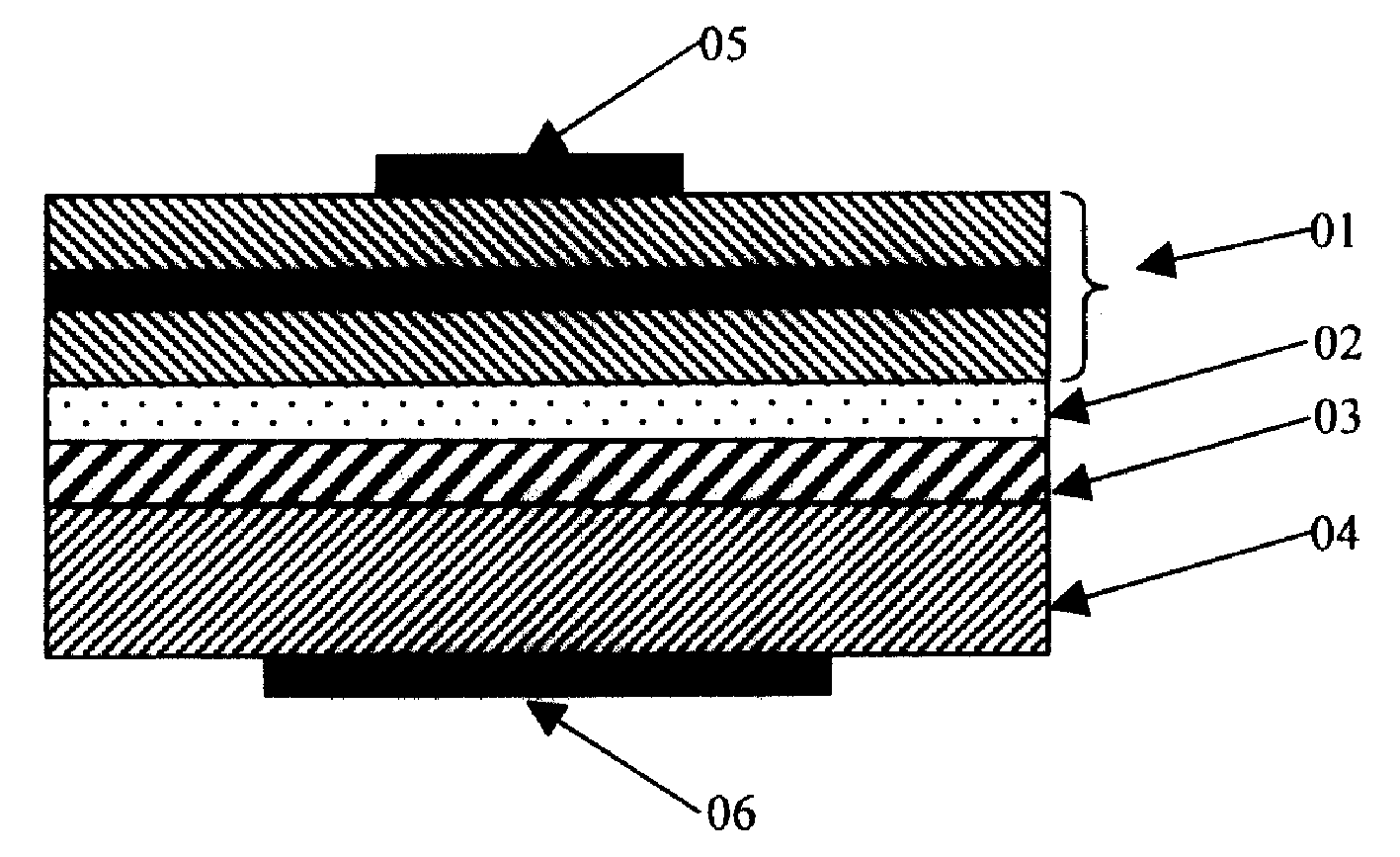
图1是本发明上下电极铟镓铝氮发光器件的剖面结构示意图。11是导电衬底,12是粘接层,13是反射层,14是铟镓铝氮半导体叠层,15、16为电极。Fig. 1 is a schematic cross-sectional structure diagram of an InGaAlN light-emitting device with upper and lower electrodes according to the present invention. 11 is a conductive substrate, 12 is an adhesive layer, 13 is a reflective layer, 14 is an InGaAlN semiconductor laminate, and 15 and 16 are electrodes.
图2是本发明中在硅(111)衬底上生长的铟镓铝氮半导体叠层及反射层和粘接层剖面结构示意图。21是硅(111)衬底,22是氮化铝缓冲层,23是未掺杂的氮化镓层,24是N型氮化镓层,25是氮化镓/铟镓氮多量子阱,26是P型氮化镓层,27是反射层,28是粘接层。Fig. 2 is a schematic cross-sectional structure diagram of an InGaAlN semiconductor laminate, a reflective layer and an adhesive layer grown on a silicon (111) substrate in the present invention. 21 is a silicon (111) substrate, 22 is an aluminum nitride buffer layer, 23 is an undoped gallium nitride layer, 24 is an N-type gallium nitride layer, and 25 is a gallium nitride/indium gallium nitrogen multiple quantum well, 26 is a p-type gallium nitride layer, 27 is a reflective layer, and 28 is an adhesive layer.
图3是本发明中导电衬底及金属粘接层剖面结构示意图。31是衬底,32是欧姆接触层,33是粘接层。Fig. 3 is a schematic cross-sectional structure diagram of a conductive substrate and a metal bonding layer in the present invention. 31 is a substrate, 32 is an ohmic contact layer, and 33 is an adhesive layer.
图4是图2中的铟镓铝氮外延片和图3中的导电衬底粘接后得到的基片剖面结构示意图。图中数字代表的层含义同图2、图3。FIG. 4 is a schematic cross-sectional structure diagram of a substrate obtained after bonding the InGaAlN epitaxial wafer in FIG. 2 and the conductive substrate in FIG. 3 . The layers represented by numbers in the figure have the same meanings as those in Figure 2 and Figure 3.
图5是图4所示的基片去除生长衬底并制作引线电极后得到的发光器件剖面结构示意图。图中数字代表的层含义同图2、图3。C1、C2为电极。FIG. 5 is a schematic cross-sectional structure diagram of a light emitting device obtained by removing the growth substrate from the substrate shown in FIG. 4 and making lead electrodes. The layers represented by numbers in the figure have the same meanings as those in Figure 2 and Figure 3. C1 and C2 are electrodes.
具体实施方式:Detailed ways:
下面用3个实施例对本发明的方法进行进一步的说明。The method of the present invention is further described below with 3 examples.
如图1所示,该器件包含一个导电衬底11,在导电衬底上依次具有一粘接金属叠层12和一光反射层13,光反射层13上为铟镓铝氮半导体叠层14,该铟镓铝氮半导体叠层14中的最下层为P型层,最上层为N型层,且该叠层铟镓铝氮材料上表面为氮面,在铟镓铝氮半导体叠层14上和导电衬底11背面各有一个欧姆电极15和16。As shown in Figure 1, the device includes a conductive substrate 11, on which there is an adhesive metal stack 12 and a light reflection layer 13 in sequence, and on the light reflection layer 13 is an InGaAlN semiconductor stack 14 , the lowermost layer in the InGaAlN semiconductor stack 14 is a P-type layer, the uppermost layer is an N-type layer, and the upper surface of the stacked InGaAlN material is a nitrogen surface, and the InGaAlN semiconductor stack 14 Ohmic electrodes 15 and 16 are provided on the upper side and on the back side of the conductive substrate 11 respectively.
实施例1:Example 1:
如图2所示,在一块2英寸的硅(111)衬底21上,用化学气相沉积法依次生长氮化铝缓冲层22、未掺杂氮化镓层23、掺硅N型氮化镓层24、5个周期的氮化镓/铟镓氮多量子阱25、掺镁P型氮化镓层26。生长完成后,把外延片在700℃氮气氛围下退火30分钟以激活镁杂质。接着用电子束蒸发法在P型层上依次蒸镀50纳米的铂27、1000纳米厚的金28。然后,如图3所示,在另一块硅(111)衬底31上蒸镀100纳米的镍32、1000纳米的金33。蒸发完成后把长有铟镓铝氮薄膜的外延片和只蒸有镍/金的硅(111)衬底对粘起来,并且在300℃下加600公斤力,使之粘接牢固,这样就得到如图4所示的结构。然后再把粘接好的衬底放入硝酸/醋酸/氢氟酸的混合溶液中腐蚀,直到生长铟镓铝氮薄膜的硅衬底被完全去除。腐蚀前先要在衬底31背面做上一层镍/金保护膜。腐蚀后,铟镓铝氮薄膜暴露出来,最外层是氮化铝缓冲层22,接着把该基片放入浓磷酸中腐蚀直到氮化铝缓冲层22和未掺杂氮化镓层23被完全去除。然后在N型氮化镓层24上蒸镀100纳米厚的金锗镍合金,并且把基片在300℃氮气氛围下下合金3分钟。然后在金锗镍电极上再蒸发1000纳米厚的金,经光刻形成直径为100微米的电极C1。然后在衬底31后面光刻形成电极C2。把基片切割成1000微米×1000微米大小的芯片,再引线封装就得到本发明的发光器件。As shown in FIG. 2, on a 2-inch silicon (111)
实施例2:Example 2:
用一块2英寸的硅(111)衬底,先在表面用光刻和ICP刻蚀的方法形成纵横交错深度为10微米的沟槽,以使表面分割成许多边长为350微米×350微米的正方形台面。然后用化学气相沉积法在衬底上依次生长氮化铝缓冲层、未掺杂氮化镓层、掺硅N型氮化镓层、5个周期的铝镓氮/铟镓氮多量子阱、掺镁P型氮化镓层。生长完成后,把外延片在760℃氮气氛围下退火20分钟以激活镁杂质。接着用电子束蒸发法在P型层上依次蒸镀100纳米的铂、500纳米厚的金、200纳米厚的金锌合金。然后在一块硅(100)衬底正反两面上都蒸镀50纳米的铂、500纳米的金、100纳米厚的金铟合金。蒸发完成后把长有铟镓铝氮薄膜的外延片和只蒸有金属层的硅(100)衬底对粘起来,在260℃下加800公斤力,使之粘接牢固。然后用ICP刻蚀把硅(111)衬底刻除直至铟镓铝氮薄膜暴露出来,此时最外层是氮化铝缓冲层。接着用ICP刻蚀方法把氮化铝缓冲层和未掺杂氮化镓层被完全刻除。然后在N型氮化镓层上蒸镀50纳米厚的钛、100纳米厚的铝,并且把基片在500℃氮气氛围合金3分钟。然后在钛/铝电极上再蒸发10纳米厚的钛和1200纳米厚的金,经光刻形成边长为100微米的正方形电极。沿着前述生长前预先形成的沟槽切开基片,就得到一颗颗独立的发光芯片,然后就可以进行引线封装并得到本发明所述的发光器件。Using a 2-inch silicon (111) substrate, first form criss-cross grooves with a depth of 10 microns on the surface by photolithography and ICP etching, so that the surface is divided into many pieces with a side length of 350 microns × 350 microns. Square top. Then, the aluminum nitride buffer layer, the undoped gallium nitride layer, the silicon-doped N-type gallium nitride layer, the aluminum gallium nitrogen/indium gallium nitrogen multiple quantum wells of 5 cycles, and the Magnesium-doped P-type GaN layer. After the growth is completed, the epitaxial wafer is annealed at 760° C. for 20 minutes under a nitrogen atmosphere to activate the magnesium impurities. Next, 100 nanometers of platinum, 500 nanometers of gold, and 200 nanometers of gold-zinc alloy are sequentially vapor-deposited on the P-type layer by electron beam evaporation. Then, 50 nanometers of platinum, 500 nanometers of gold, and 100 nanometers of gold-indium alloy are evaporated on both sides of a silicon (100) substrate. After the evaporation is completed, the epitaxial wafer with the InGaAlN film and the silicon (100) substrate with only the metal layer evaporated are bonded together, and 800 kilograms of force are applied at 260 ° C to make the bonding firm. Then use ICP etching to etch away the silicon (111) substrate until the InGaAlN thin film is exposed, and at this time the outermost layer is the AlN buffer layer. Then the aluminum nitride buffer layer and the undoped gallium nitride layer are completely etched away by ICP etching method. Then, 50 nanometers of titanium and 100 nanometers of aluminum were vapor-deposited on the N-type GaN layer, and the substrate was alloyed in a nitrogen atmosphere at 500° C. for 3 minutes. Then evaporate 10 nanometers of titanium and 1200 nanometers of gold on the titanium/aluminum electrode, and form a square electrode with a side length of 100 micrometers by photolithography. By cutting the substrate along the pre-formed grooves before growth, individual light-emitting chips can be obtained, and then lead packaging can be performed to obtain the light-emitting device of the present invention.
实施例3:Example 3:
在一块2英寸的硅(111)衬底上,用化学气相沉积法依次生长氮化铝缓冲层、未掺杂氮化镓层、掺硅N型氮化镓层、5个周期的铟镓铝氮/铟镓氮多量子阱、掺镁P型氮化镓层。生长完成后,把外延片在700℃氮气氛围下退火30分钟以激活镁杂质。接着用电子束蒸发法在P型层上依次蒸镀5纳米的铂、5纳米厚的镍、10纳米厚的金,并在550℃氮氧混合气中合金3分钟。然后再蒸镀500纳米厚的金。在一块抛光好的铜衬底上蒸500纳米的金锡合金。蒸发完成后把外延片和镀有金锡的铜衬底对粘起来,并且在300℃下加500公斤力,使之粘接牢固。然后用ICP刻蚀把硅衬底完全去除。接着把氮化铝缓冲层和未掺杂氮化镓层完全去除。然后在N型氮化镓层上蒸镀100纳米厚的金锗镍合金,并且把基片在300℃氮气氛围下下合金3分钟。然后在金锗镍电极上再蒸发100纳米厚的金,经光刻形成直径为80微米的电极。把基片切割成200微米×200微米的芯片并引线封装就得到本发明的发光器件。On a 2-inch silicon (111) substrate, an aluminum nitride buffer layer, an undoped gallium nitride layer, a silicon-doped N-type gallium nitride layer, and five cycles of indium gallium aluminum were sequentially grown by chemical vapor deposition. Nitrogen/InGaN MQW, Mg-doped P-type GaN layer. After the growth is completed, the epitaxial wafer is annealed at 700° C. for 30 minutes under a nitrogen atmosphere to activate the magnesium impurities. Then, 5 nanometers of platinum, 5 nanometers of nickel, and 10 nanometers of gold were sequentially vapor-deposited on the P-type layer by electron beam evaporation, and alloyed in a nitrogen-oxygen mixture at 550° C. for 3 minutes. Gold was then vapor-deposited to a thickness of 500 nanometers. 500 nm gold-tin alloy was evaporated on a polished copper substrate. After the evaporation is completed, the epitaxial wafer and the copper substrate plated with gold and tin are bonded together, and a force of 500 kg is applied at 300 ° C to make the bonding firm. The silicon substrate is then completely removed by ICP etching. Then the aluminum nitride buffer layer and the undoped gallium nitride layer are completely removed. Then on the N-type gallium nitride layer, 100 nanometers thick gold-germanium-nickel alloy was vapor-deposited, and the substrate was alloyed for 3 minutes under nitrogen atmosphere at 300°C. Then evaporate 100 nanometers of gold on the gold-germanium-nickel electrode, and form an electrode with a diameter of 80 microns by photolithography. The light-emitting device of the present invention is obtained by cutting the substrate into chips of 200 micrometers x 200 micrometers and packaging them with wires.
Claims (9)
Priority Applications (7)
| Application Number | Priority Date | Filing Date | Title |
|---|---|---|---|
| CNB2005100263065A CN100372137C (en) | 2005-05-27 | 2005-05-27 | InGaAlN light-emitting device with upper and lower electrode structure and manufacturing method thereof |
| US11/915,304 US8384100B2 (en) | 2005-05-27 | 2006-05-26 | InGaAIN light-emitting device and manufacturing method thereof |
| PCT/CN2006/001100 WO2006125396A1 (en) | 2005-05-27 | 2006-05-26 | InGaAlN LIGHT-EMITTING DEVICE AND MANUFACTURING METHOD THEREOF |
| EP06741988.7A EP1885001A4 (en) | 2005-05-27 | 2006-05-26 | GAIN ELECTROLUMINESCENT DEVICE AND METHOD FOR MANUFACTURING THE SAME |
| JP2008512675A JP2008543032A (en) | 2005-05-27 | 2006-05-26 | InGaAlN light emitting device and manufacturing method thereof |
| KR1020077026564A KR20080015794A (en) | 2005-05-27 | 2006-05-26 | イ nGaAlN light emitting device and manufacturing method thereof |
| JP2012150559A JP2012212929A (en) | 2005-05-27 | 2012-07-04 | InGaAlN LIGHT-EMITTING DEVICE AND METHOD OF MANUFACTURING THE SAME |
Applications Claiming Priority (1)
| Application Number | Priority Date | Filing Date | Title |
|---|---|---|---|
| CNB2005100263065A CN100372137C (en) | 2005-05-27 | 2005-05-27 | InGaAlN light-emitting device with upper and lower electrode structure and manufacturing method thereof |
Publications (2)
| Publication Number | Publication Date |
|---|---|
| CN1694271A true CN1694271A (en) | 2005-11-09 |
| CN100372137C CN100372137C (en) | 2008-02-27 |
Family
ID=35353147
Family Applications (1)
| Application Number | Title | Priority Date | Filing Date |
|---|---|---|---|
| CNB2005100263065A Expired - Lifetime CN100372137C (en) | 2005-05-27 | 2005-05-27 | InGaAlN light-emitting device with upper and lower electrode structure and manufacturing method thereof |
Country Status (6)
| Country | Link |
|---|---|
| US (1) | US8384100B2 (en) |
| EP (1) | EP1885001A4 (en) |
| JP (2) | JP2008543032A (en) |
| KR (1) | KR20080015794A (en) |
| CN (1) | CN100372137C (en) |
| WO (1) | WO2006125396A1 (en) |
Cited By (5)
| Publication number | Priority date | Publication date | Assignee | Title |
|---|---|---|---|---|
| WO2010020069A1 (en) * | 2008-08-19 | 2010-02-25 | Lattice Power (Jiangxi) Corporation | METHOD FOR FABRICATING InGaAlN LIGHT-EMITTING DIODES WITH A METAL SUBSTRATE |
| WO2010020077A1 (en) * | 2008-08-22 | 2010-02-25 | Lattice Power (Jiangxi) Corporation | Method for fabricating ingaain light-emitting device on a combined substrate |
| CN101636820B (en) * | 2007-03-28 | 2011-09-07 | 松下电器产业株式会社 | Ohmic electrode structure and semiconductor element |
| CN101295758B (en) * | 2007-04-29 | 2013-03-06 | 晶能光电(江西)有限公司 | Indium gallium aluminum nitrogen illuminating device containing carbon based underlay and its production method |
| CN104037287A (en) * | 2014-06-10 | 2014-09-10 | 广州市众拓光电科技有限公司 | LED epitaxial wafer grown on Si substrate and preparation method thereof |
Families Citing this family (17)
| Publication number | Priority date | Publication date | Assignee | Title |
|---|---|---|---|---|
| CN100375303C (en) | 2005-10-27 | 2008-03-12 | 晶能光电(江西)有限公司 | Ohmic electrode containing gold germanium and nickel, indium gallium aluminum nitrogen semiconductor light-emitting element and manufacturing method |
| US7781780B2 (en) * | 2008-03-31 | 2010-08-24 | Bridgelux, Inc. | Light emitting diodes with smooth surface for reflective electrode |
| WO2009129353A1 (en) * | 2008-04-15 | 2009-10-22 | Purdue Research Foundation | Metallized silicon substrate for indium gallium nitride light-emitting diode |
| DE102008030584A1 (en) | 2008-06-27 | 2009-12-31 | Osram Opto Semiconductors Gmbh | Method for producing an optoelectronic component and optoelectronic component |
| US8525200B2 (en) | 2008-08-18 | 2013-09-03 | Taiwan Semiconductor Manufacturing Company, Ltd. | Light-emitting diode with non-metallic reflector |
| US8188496B2 (en) | 2008-11-06 | 2012-05-29 | Samsung Led Co., Ltd. | Semiconductor light emitting device including substrate having protection layers and method for manufacturing the same |
| KR101004858B1 (en) * | 2008-11-06 | 2010-12-28 | 삼성엘이디 주식회사 | Compound Semiconductor Light-Emitting Device and Manufacturing Method Thereof |
| ATE555494T1 (en) | 2009-02-19 | 2012-05-15 | S O I Tec Silicon | RELAXATION AND TRANSFER OF STRESSED MATERIAL LAYERS |
| US8642369B2 (en) * | 2009-03-03 | 2014-02-04 | Zn Technology, Inc. | Vertically structured LED by integrating nitride semiconductors with Zn(Mg,Cd,Be)O(S,Se) and method for making same |
| TW201112440A (en) * | 2009-09-29 | 2011-04-01 | Ubilux Optoelectronics Corp | Manufacturing method of vertical light emitting diode |
| US9343641B2 (en) | 2011-08-02 | 2016-05-17 | Manutius Ip, Inc. | Non-reactive barrier metal for eutectic bonding process |
| US9012939B2 (en) * | 2011-08-02 | 2015-04-21 | Kabushiki Kaisha Toshiba | N-type gallium-nitride layer having multiple conductive intervening layers |
| US9053930B2 (en) | 2012-04-17 | 2015-06-09 | International Business Machines Corporation | Heterogeneous integration of group III nitride on silicon for advanced integrated circuits |
| US9099381B2 (en) | 2012-11-15 | 2015-08-04 | International Business Machines Corporation | Selective gallium nitride regrowth on (100) silicon |
| US9048173B2 (en) | 2012-11-15 | 2015-06-02 | International Business Machines Corporation | Dual phase gallium nitride material formation on (100) silicon |
| CN116825925A (en) * | 2018-12-24 | 2023-09-29 | 泉州三安半导体科技有限公司 | Light-emitting diode and manufacturing method thereof |
| US11127595B2 (en) | 2019-09-19 | 2021-09-21 | Microsoft Technology Licensing, Llc | Method for bonding a semiconductor substrate to a carrier |
Family Cites Families (46)
| Publication number | Priority date | Publication date | Assignee | Title |
|---|---|---|---|---|
| JPS6466977A (en) * | 1987-09-08 | 1989-03-13 | Oki Electric Ind Co Ltd | Manufacture of optical semiconductor device |
| JP2704181B2 (en) * | 1989-02-13 | 1998-01-26 | 日本電信電話株式会社 | Method for growing compound semiconductor single crystal thin film |
| JP2503920B2 (en) * | 1993-10-05 | 1996-06-05 | 日本電気株式会社 | Optical semiconductor device and manufacturing method thereof. |
| JPH10173226A (en) * | 1996-12-06 | 1998-06-26 | Rohm Co Ltd | Semiconductor light-emitting element |
| JPH118414A (en) * | 1997-06-18 | 1999-01-12 | Sony Corp | Semiconductor device and semiconductor light emitting device |
| JP2000174393A (en) * | 1998-12-04 | 2000-06-23 | Fuji Electric Co Ltd | Group III nitride semiconductor, method of manufacturing the same, and group III nitride semiconductor device |
| US20010042866A1 (en) * | 1999-02-05 | 2001-11-22 | Carrie Carter Coman | Inxalygazn optical emitters fabricated via substrate removal |
| JP3702700B2 (en) * | 1999-03-31 | 2005-10-05 | 豊田合成株式会社 | Group III nitride compound semiconductor device and method for manufacturing the same |
| JP2001102632A (en) * | 1999-10-01 | 2001-04-13 | Advantest Corp | Compound semiconductor device and manufacturing method therefor |
| US6287882B1 (en) * | 1999-10-04 | 2001-09-11 | Visual Photonics Epitaxy Co., Ltd. | Light emitting diode with a metal-coated reflective permanent substrate and the method for manufacturing the same |
| JP4432180B2 (en) * | 1999-12-24 | 2010-03-17 | 豊田合成株式会社 | Group III nitride compound semiconductor manufacturing method, group III nitride compound semiconductor device, and group III nitride compound semiconductor |
| JP2001267242A (en) * | 2000-03-14 | 2001-09-28 | Toyoda Gosei Co Ltd | Group III nitride compound semiconductor and method of manufacturing the same |
| JP2001284641A (en) * | 2000-03-31 | 2001-10-12 | Sony Corp | Image display device |
| CN1252837C (en) * | 2000-04-26 | 2006-04-19 | 奥斯兰姆奥普托半导体股份有限两合公司 | Light emitting diode chip on GaN substrate and method of manufacturing light emitting diode element using light emitting diode chip on GaN substrate |
| JP2002057411A (en) * | 2000-08-09 | 2002-02-22 | Ricoh Co Ltd | Semiconductor laser device and optical pickup |
| US6791119B2 (en) * | 2001-02-01 | 2004-09-14 | Cree, Inc. | Light emitting diodes including modifications for light extraction |
| CN1185720C (en) * | 2001-03-05 | 2005-01-19 | 全新光电科技股份有限公司 | A light-emitting diode coated with a metal mirror film substrate and its manufacturing method |
| TW523939B (en) * | 2001-11-07 | 2003-03-11 | Nat Univ Chung Hsing | High-efficient light emitting diode and its manufacturing method |
| JP4078830B2 (en) * | 2001-11-29 | 2008-04-23 | ソニー株式会社 | Display device and manufacturing method of display device |
| JP2003174194A (en) * | 2001-12-07 | 2003-06-20 | Sharp Corp | Nitride based semiconductor light emitting device and method of manufacturing the same |
| TWI278995B (en) * | 2002-01-28 | 2007-04-11 | Nichia Corp | Nitride semiconductor element with a supporting substrate and a method for producing a nitride semiconductor element |
| US6869820B2 (en) * | 2002-01-30 | 2005-03-22 | United Epitaxy Co., Ltd. | High efficiency light emitting diode and method of making the same |
| JP3960815B2 (en) * | 2002-02-12 | 2007-08-15 | シャープ株式会社 | Semiconductor light emitting device |
| JP3896027B2 (en) * | 2002-04-17 | 2007-03-22 | シャープ株式会社 | Nitride-based semiconductor light-emitting device and method for manufacturing the same |
| US6919585B2 (en) * | 2002-05-17 | 2005-07-19 | Lumei Optoelectronics, Inc. | Light-emitting diode with silicon carbide substrate |
| JP2004088083A (en) * | 2002-06-25 | 2004-03-18 | Matsushita Electric Ind Co Ltd | Semiconductor light emitting device, method of manufacturing the same, and method of mounting the same |
| KR101030068B1 (en) * | 2002-07-08 | 2011-04-19 | 니치아 카가쿠 고교 가부시키가이샤 | Nitride semiconductor device manufacturing method and nitride semiconductor device |
| US6642092B1 (en) * | 2002-07-11 | 2003-11-04 | Sharp Laboratories Of America, Inc. | Thin-film transistors formed on a metal foil substrate |
| JP2004047748A (en) * | 2002-07-12 | 2004-02-12 | Stanley Electric Co Ltd | Light emitting diode |
| JP2004079972A (en) * | 2002-08-22 | 2004-03-11 | Fuji Photo Film Co Ltd | Surface-emitting light emitting device |
| JP3997523B2 (en) * | 2002-11-28 | 2007-10-24 | 信越半導体株式会社 | Light emitting element |
| KR100495215B1 (en) * | 2002-12-27 | 2005-06-14 | 삼성전기주식회사 | VERTICAL GaN LIGHT EMITTING DIODE AND METHOD OF PRODUCING THE SAME |
| TWI230473B (en) * | 2003-03-10 | 2005-04-01 | Sanken Electric Co Ltd | Semiconductor light emitting device and manufacturing method thereof |
| JP4325232B2 (en) * | 2003-03-18 | 2009-09-02 | 日亜化学工業株式会社 | Nitride semiconductor device |
| JP4217093B2 (en) * | 2003-03-27 | 2009-01-28 | スタンレー電気株式会社 | Semiconductor light emitting device and manufacturing method thereof |
| TWI287878B (en) * | 2003-04-16 | 2007-10-01 | Arima Optoelectronics Corp | Light-emitting diodes and method of manufacturing same using metal bonding technique |
| US20040231590A1 (en) * | 2003-05-19 | 2004-11-25 | Ovshinsky Stanford R. | Deposition apparatus for the formation of polycrystalline materials on mobile substrates |
| JP2005072148A (en) * | 2003-08-21 | 2005-03-17 | Mitsubishi Cable Ind Ltd | Nitride semiconductor devices |
| FR2859312B1 (en) * | 2003-09-02 | 2006-02-17 | Soitec Silicon On Insulator | MULTIFUNCTIONAL METAL SEAL |
| CN100355096C (en) * | 2003-09-23 | 2007-12-12 | 晶元光电股份有限公司 | Manufacturing method of light emitting element having heat absorbing layer |
| JP2005109220A (en) * | 2003-09-30 | 2005-04-21 | Shin Etsu Handotai Co Ltd | Light-emitting element |
| TW200520266A (en) * | 2003-11-21 | 2005-06-16 | Sanken Electric Co Ltd | Semiconductor luminous element and manufacturing method of the same |
| JP2005223165A (en) * | 2004-02-06 | 2005-08-18 | Sanyo Electric Co Ltd | Nitride-based light emitting device |
| KR101119019B1 (en) * | 2004-12-14 | 2012-03-12 | 주식회사 엘지실트론 | GaN semiconductor and manufacturing methods for the same |
| KR100638818B1 (en) * | 2005-05-19 | 2006-10-27 | 삼성전기주식회사 | Nitride semiconductor light emitting device |
| US8334155B2 (en) * | 2005-09-27 | 2012-12-18 | Philips Lumileds Lighting Company Llc | Substrate for growing a III-V light emitting device |
-
2005
- 2005-05-27 CN CNB2005100263065A patent/CN100372137C/en not_active Expired - Lifetime
-
2006
- 2006-05-26 KR KR1020077026564A patent/KR20080015794A/en not_active Ceased
- 2006-05-26 WO PCT/CN2006/001100 patent/WO2006125396A1/en not_active Ceased
- 2006-05-26 JP JP2008512675A patent/JP2008543032A/en active Pending
- 2006-05-26 US US11/915,304 patent/US8384100B2/en active Active
- 2006-05-26 EP EP06741988.7A patent/EP1885001A4/en not_active Ceased
-
2012
- 2012-07-04 JP JP2012150559A patent/JP2012212929A/en active Pending
Cited By (6)
| Publication number | Priority date | Publication date | Assignee | Title |
|---|---|---|---|---|
| CN101636820B (en) * | 2007-03-28 | 2011-09-07 | 松下电器产业株式会社 | Ohmic electrode structure and semiconductor element |
| CN101295758B (en) * | 2007-04-29 | 2013-03-06 | 晶能光电(江西)有限公司 | Indium gallium aluminum nitrogen illuminating device containing carbon based underlay and its production method |
| WO2010020069A1 (en) * | 2008-08-19 | 2010-02-25 | Lattice Power (Jiangxi) Corporation | METHOD FOR FABRICATING InGaAlN LIGHT-EMITTING DIODES WITH A METAL SUBSTRATE |
| WO2010020077A1 (en) * | 2008-08-22 | 2010-02-25 | Lattice Power (Jiangxi) Corporation | Method for fabricating ingaain light-emitting device on a combined substrate |
| CN104037287A (en) * | 2014-06-10 | 2014-09-10 | 广州市众拓光电科技有限公司 | LED epitaxial wafer grown on Si substrate and preparation method thereof |
| CN104037287B (en) * | 2014-06-10 | 2017-01-11 | 广州市众拓光电科技有限公司 | LED epitaxial wafer grown on Si substrate and preparation method thereof |
Also Published As
| Publication number | Publication date |
|---|---|
| EP1885001A1 (en) | 2008-02-06 |
| JP2012212929A (en) | 2012-11-01 |
| US20090026473A1 (en) | 2009-01-29 |
| KR20080015794A (en) | 2008-02-20 |
| CN100372137C (en) | 2008-02-27 |
| JP2008543032A (en) | 2008-11-27 |
| US8384100B2 (en) | 2013-02-26 |
| WO2006125396A1 (en) | 2006-11-30 |
| EP1885001A4 (en) | 2015-07-01 |
Similar Documents
| Publication | Publication Date | Title |
|---|---|---|
| CN100372137C (en) | InGaAlN light-emitting device with upper and lower electrode structure and manufacturing method thereof | |
| KR101254539B1 (en) | Vertical structure semiconductor devices | |
| CN101295758B (en) | Indium gallium aluminum nitrogen illuminating device containing carbon based underlay and its production method | |
| CN100375303C (en) | Ohmic electrode containing gold germanium and nickel, indium gallium aluminum nitrogen semiconductor light-emitting element and manufacturing method | |
| US7319248B2 (en) | High brightness light emitting diode | |
| US9224910B2 (en) | Supporting substrate for preparing semiconductor light-emitting device and semiconductor light-emitting device using supporting substrates | |
| KR101198758B1 (en) | Vertical structured semiconductor light emitting device and method for producing thereof | |
| CN102255013B (en) | Method for making light-emitting diode with vertical structure through stripping GaN based epitaxial layer and sapphire substrate by using wet process | |
| KR20100008123A (en) | Vertical light emitting devices with the support composed of double heat-sinking layer | |
| CN101807636B (en) | Nitride semiconductor light-emitting element | |
| CN1905225A (en) | Nitride-based compound semiconductor light emitting device and method of fabricating the same | |
| KR100916366B1 (en) | Supporting substrates for semiconductor light emitting device and method of manufacturing vertical structured semiconductor light emitting device using the supporting substrates | |
| CN100474642C (en) | Indium gallium aluminium nitrogen semi-conductor luminous element containing metallic chromium substrate and manufacturing method thereof | |
| KR100999548B1 (en) | A support substrate for manufacturing a semiconductor light emitting device having a vertical structure, a method for manufacturing a semiconductor light emitting device having a vertical structure and a semiconductor light emitting device having a vertical structure | |
| KR100886110B1 (en) | Support substrate for semiconductor light emitting device and method for manufacturing semiconductor light emitting device having vertical structure using same | |
| KR100832102B1 (en) | Structure for Light-Emitting Element and Manufacturing Method of Light-Emitting Element | |
| KR101231118B1 (en) | Supporting substrates for semiconductor light emitting device and high-performance vertical structured semiconductor light emitting devices using supporting substrates | |
| KR101499954B1 (en) | fabrication of vertical structured light emitting diodes using group 3 nitride-based semiconductors and its related methods | |
| CN1527409A (en) | Manufacturing method of small-sized gallium nitride-based blue and green light-emitting diode tube cores | |
| CN1525577A (en) | Manufacturing method of gallium nitride-based light-emitting diode N-type layer ohmic contact electrode | |
| KR101171855B1 (en) | Supporting substrates for semiconductor light emitting device and high-performance vertical structured semiconductor light emitting devices using supporting substrates | |
| CN1780001A (en) | Semiconductor light emitting element and manufacturing method thereof | |
| CN111968907A (en) | Nitrogen polarity III group nitride coarsening method | |
| JP2006100793A (en) | Compound semiconductor light emitting device |
Legal Events
| Date | Code | Title | Description |
|---|---|---|---|
| C06 | Publication | ||
| PB01 | Publication | ||
| C10 | Entry into substantive examination | ||
| SE01 | Entry into force of request for substantive examination | ||
| ASS | Succession or assignment of patent right |
Owner name: JINGNENG PHOTOELECTRIC( JIANGXI ) CO., LTD. Free format text: FORMER OWNER: NANCHANG UNIV. Effective date: 20060804 |
|
| C41 | Transfer of patent application or patent right or utility model | ||
| TA01 | Transfer of patent application right |
Effective date of registration: 20060804 Address after: 330047 No. 235 East Nanjing Road, Jiangxi, Nanchang Applicant after: Lattice Power (JiangXi) Corp. Address before: 330047 material research institute, Nanchang University, 235 East Nanjing Road, Nanchang, Jiangxi Applicant before: Nanchang University |
|
| C14 | Grant of patent or utility model | ||
| GR01 | Patent grant | ||
| EE01 | Entry into force of recordation of patent licensing contract |
Application publication date: 20051109 Assignee: LATTICE POWER (CHANGZHOU) Corp. Assignor: LATTICE POWER (JIANGXI) Corp. Contract record no.: 2012360000083 Denomination of invention: Indium gallium aluminum nitrogen luminous device with up-down cathode strucure and manufacturing method thereof Granted publication date: 20080227 License type: Common License Record date: 20121213 |
|
| LICC | Enforcement, change and cancellation of record of contracts on the licence for exploitation of a patent or utility model | ||
| EC01 | Cancellation of recordation of patent licensing contract |
Assignee: LATTICE POWER (CHANGZHOU) Corp. Assignor: LATTICE POWER (JIANGXI) Corp. Contract record no.: 2012360000083 Date of cancellation: 20220228 |
|
| EC01 | Cancellation of recordation of patent licensing contract | ||
| CP01 | Change in the name or title of a patent holder |
Address after: 330047 No. 235 East Nanjing Road, Jiangxi, Nanchang Patentee after: Jingneng optoelectronics Co.,Ltd. Address before: 330047 No. 235 East Nanjing Road, Jiangxi, Nanchang Patentee before: LATTICE POWER (JIANGXI) Corp. |
|
| CP01 | Change in the name or title of a patent holder | ||
| CX01 | Expiry of patent term | ||
| CX01 | Expiry of patent term |
Granted publication date: 20080227 |