CN1551505A - Versatile charge sampling circuits - Google Patents
Versatile charge sampling circuits Download PDFInfo
- Publication number
- CN1551505A CN1551505A CNA2004100598399A CN200410059839A CN1551505A CN 1551505 A CN1551505 A CN 1551505A CN A2004100598399 A CNA2004100598399 A CN A2004100598399A CN 200410059839 A CN200410059839 A CN 200410059839A CN 1551505 A CN1551505 A CN 1551505A
- Authority
- CN
- China
- Prior art keywords
- signal
- circuit
- output
- bpcs
- input
- Prior art date
- Legal status (The legal status is an assumption and is not a legal conclusion. Google has not performed a legal analysis and makes no representation as to the accuracy of the status listed.)
- Pending
Links
Images


Classifications
-
- H—ELECTRICITY
- H04—ELECTRIC COMMUNICATION TECHNIQUE
- H04B—TRANSMISSION
- H04B1/00—Details of transmission systems, not covered by a single one of groups H04B3/00 - H04B13/00; Details of transmission systems not characterised by the medium used for transmission
- H04B1/0003—Software-defined radio [SDR] systems, i.e. systems wherein components typically implemented in hardware, e.g. filters or modulators/demodulators, are implented using software, e.g. by involving an AD or DA conversion stage such that at least part of the signal processing is performed in the digital domain
- H04B1/0007—Software-defined radio [SDR] systems, i.e. systems wherein components typically implemented in hardware, e.g. filters or modulators/demodulators, are implented using software, e.g. by involving an AD or DA conversion stage such that at least part of the signal processing is performed in the digital domain wherein the AD/DA conversion occurs at radiofrequency or intermediate frequency stage
-
- G—PHYSICS
- G11—INFORMATION STORAGE
- G11C—STATIC STORES
- G11C27/00—Electric analogue stores, e.g. for storing instantaneous values
- G11C27/02—Sample-and-hold arrangements
- G11C27/024—Sample-and-hold arrangements using a capacitive memory element
-
- H—ELECTRICITY
- H04—ELECTRIC COMMUNICATION TECHNIQUE
- H04B—TRANSMISSION
- H04B1/00—Details of transmission systems, not covered by a single one of groups H04B3/00 - H04B13/00; Details of transmission systems not characterised by the medium used for transmission
-
- H—ELECTRICITY
- H04—ELECTRIC COMMUNICATION TECHNIQUE
- H04B—TRANSMISSION
- H04B1/00—Details of transmission systems, not covered by a single one of groups H04B3/00 - H04B13/00; Details of transmission systems not characterised by the medium used for transmission
- H04B1/06—Receivers
- H04B1/16—Circuits
- H04B1/26—Circuits for superheterodyne receivers
- H04B1/28—Circuits for superheterodyne receivers the receiver comprising at least one semiconductor device having three or more electrodes
Landscapes
- Engineering & Computer Science (AREA)
- Computer Networks & Wireless Communication (AREA)
- Signal Processing (AREA)
- Analogue/Digital Conversion (AREA)
- Networks Using Active Elements (AREA)
- Peptides Or Proteins (AREA)
- Separation By Low-Temperature Treatments (AREA)
- Transition And Organic Metals Composition Catalysts For Addition Polymerization (AREA)
- Glass Compositions (AREA)
Abstract
A charge sampling (CS) circuit (1), comprising a control signal generator (4) for controlling an analog input signal to the charge sampling circuit (1) to be integrated by an integrator (3) during a sampling phase responsive to a sampling signal from the control signal generator , wherein the current of the analog input signal is integrated to an integrated charge for producing a proportional voltage or current sample at a signal output at the end of the sampling phase.
Description
Background of invention
Voltage sampling is used for mould/number (A/D) conversion traditionally.In the voltage sampling device, between a signal source and a capacitor, a sampling switch is set.Between two sampling times, the voltage of this capacitor is tracking signal voltage exactly.At sampling time, disconnect this switch to keep condenser voltage.When improving signal frequency, it is all the more difficult that these two processes become.For given precision, thermal noise and switching noise decision minimum are allowed electric capacity, and tracking velocity decision maximum is allowed electric capacity or switch resistance.When this maximum then become during less than this minimum value impossible.In addition, it is true that clock jitter and limited turn-off speed (non-zero sampling aperture) make sampling timing uncertainty.In fact, the bandwidth of voltage sampling circuit must be much larger than signal bandwidth.This makes that the direct sampling of high frequency radio signal is very difficult.Double sampling can reduce sampling rate, but can not reduce the bandwidth of sampling circuit and can not reduce little clock is risen and fallen and the requirement of little sampling aperture.
Summary of the invention
The purpose of this invention is to provide a kind of modified model sampling circuit of overcoming the problems referred to above and a kind of method of sampled analog signal.
In order to reach described purpose, the invention provides a kind of electric charge sampling (CS) circuit, it comprises that is used to control the control-signals generator to the analog input signal of this charge sampling circuits, this analog input signal responds a sampled signal from this control-signals generator by an integrator integration during a sampling phase, wherein the electric current of this analog input signal is integrated into integral charge to generate the sampling of a ratio-voltage or electric current in the signal output part place when this sampling phase finishes.
Of the present invention one more specifically purpose provide a kind of method and sampling circuit that is used for bandpass sampling.
This purpose reaches by a bandpass sampling (BPCS) circuit, and it comprises a control-signals generator that is used to control first end and second end of a differential analog signal, and this differential analog signal is at a weighting and sampling (W﹠amp; S) during the stage response from the W﹠amp of this control-signals generator; The S signal is by a W﹠amp; The S element weights is wherein only as a described W﹠amp; The S signal is in W﹠amp; The electric current of S this analog signal during the stage is just by described W﹠amp; The S element, and described control-signals generator is applicable at W﹠amp; This W﹠amp of control during the S stage; The output signal of S element is by an integrator integration, wherein this W﹠amp; The electric current of the output signal of S element is integrated into integral charge with at this W﹠amp; When finishing, the S stage generates a ratio-voltage or electric current sampling in signal output part.
The present invention another more specifically purpose provide a kind of secondary BPCS circuit.This reaches by a foundation secondary BPCS of the present invention circuit, and it comprises: a foundation BPCS circuit of the present invention is used to generate the signal sampling that has first sampling rate; A chopper circuit is used for by in time at the signal output part place or the pair of output place of a BPCS circuit signal from a BPCS circuit being carried out copped wave symmetrically with the equal clock signal frequency of this first sampling rate; A difference output amplifier is used for the signal of difference ground amplification from this chopper circuit; The signal output part of first signal input part of wherein said the 2nd BPCS and secondary signal input and described amplifier (41) is to being connected, in order to generate signal sampling at signal output part or output to sentencing one second sampling rate.
Another specific purposes of the present invention provide a kind of front end sampling radio receiver.This reaches by a kind of foundation front end of the present invention sampling radio receiver, and it comprises: one is used to receive and the low pass filter of filtering radio signal, and its bandwidth is up to two times of clock frequency; A low noise amplifier is used for generating the radio signal that a difference is amplified from this filtered signal; A local oscillator is used for generating an I clock signal at its signal output part; A pi/2 phase shifter, an one signal input part is connected with this local oscillator, is used for generating at its signal output part place amplitude but Q clock signal of phase shift pi/2 identical with the I clock signal; The two right ends of signal output of wherein said low noise amplifier all are connected to respectively on a BPCS circuit and the 2nd BPCS circuit, described I clock signal output terminal is connected to the input end of clock of a described BPCS circuit, and the Q clock signal output terminal is connected to the input end of clock of the 2nd BPCS circuit, in order at the signal output part of a BPCS circuit or output to locating to generate the baseband I sampling of this radio signal, and at the signal output part of described the 2nd BPCS circuit or output to locating to generate the base band Q sampling of this radio signal.
Advantage according to charge sampling circuits of the present invention is that the bandwidth of this charge sampling circuits needn't be much larger than signal bandwidth.Another important background is that for a radio signal, no matter how high carrier frequency is, signal bandwidth (base band) remains the sub-fraction of DC (direct current) to the whole frequency band between the carrier frequency.Thereby needn't change whole frequency band, but only need change the frequency band that has signal.
Under given accuracy, the signal frequency that can be higher than by the signal frequency of this CS circuit or this BPCS circuit sampling or can sample far above the voltage sampling circuit.
The sampling electric capacity that uses in this CS circuit or this BPCS circuit greater than or the sampling electric capacity that uses in the voltage sampling circuit, thereby provide the advantage of low noise and low clock and electric charge feedthrough.
Each BPCS circuit is a filter, a frequency mixer and a sampler simultaneously, and this is the simplified radio receiver greatly.
This BPCS circuit can directly be worked on radio frequency band, and this makes the high digital radio receiver that has front end sampling and A/D conversion become possibility.
The centre frequency of BPCS circuit and bandwidth all are easy to be programmed.Bandwidth can be by required narrow as far as possible, is equal to have a unlimited Q value.
This CS circuit and this BPCS circuit are simple, and can easily realize in CMOS or other technology.
For the system-on-a-chip purpose of the simple and high Digitallized system structure of needs, this technology is very useful.
Emphasize to be pointed out that, term when using in this manual " comprises " existence that is used to stipulate mentioned characteristic, integer, step or parts, but it is not got rid of and exists or add one or more other characteristic, integer, step, parts and their combinations.
Brief description of drawings
In order to explain the present invention and various advantage of the present invention and characteristics in more detail, describe a preferred embodiment in detail below with reference to each accompanying drawing, in the accompanying drawings:
Figure 1A is the calcspar according to one first embodiment of a kind of electric charge sampling (CS) circuit of the present invention,
Figure 1B illustrates the work wave of electric charge sampling (CS) circuit among Figure 1A,
Fig. 1 C illustrates the frequency response of electric charge sampling (CS) circuit among Figure 1A,
Fig. 2 A is first according to a kind of band energising lotus sampling (BPCS) circuit of the present invention
The calcspar of embodiment,
Fig. 2 B illustrates the work wave of band energising lotus sampling (BPCS) circuit among Fig. 2 A,
Fig. 3 is the calcspar according to one first embodiment of a kind of difference BPCS circuit of the present invention,
Fig. 4 is the calcspar according to one first embodiment of a kind of difference BPCS circuit in parallel of the present invention,
Fig. 5 illustrates the illustration that is used for according to the filter function of BPCS circuit of the present invention,
Fig. 6 A is the ideal frequency response of the constant weighting BPCS circuit of foundation n=10 of the present invention,
Fig. 6 B is the output sampling waveform of the constant weighting BPCS circuit of n=10,
Fig. 7 A is the ideal frequency response of the constant weighting BPCS circuit of n=50,
Fig. 7 B is the ideal frequency response of the constant weighting BPCS circuit of n=500,
Fig. 8 A is the ideal frequency response of the linear weighted function BPCS circuit of n=50,
Fig. 8 B is the ideal frequency response of the linear weighted function BPCS circuit of n=500,
Fig. 9 A is the ideal frequency response of Gauss's weighting BPCS circuit of n=75 and n=87,
Fig. 9 B is the ideal frequency response of Gauss's weighting BPCS circuit of n=750 and n=870,
Figure 10 is the circuit diagram of first embodiment of the difference BPCS circuit among Fig. 3,
Figure 11 A illustrates the circuit diagram according to n=10 constant weighting under 1000 megahertzes of Figure 10,
Figure 11 B illustrates the frequency response that the circuit among Figure 11 A produces,
Figure 12 A illustrates the circuit diagram in 1000 megahertz lower linear weightings according to the n=59 of Figure 10,
Figure 12 B is the frequency response that the circuit among Figure 12 A produces,
Figure 13 A is according to the n=599 of Figure 10 circuit diagram in 1000 megahertz lower linear weightings,
Figure 13 B is the frequency response that the circuit among Figure 13 A produces,
Figure 14 A is a kind of circuit diagram of single-ended active integrator,
Figure 14 B is a kind of circuit diagram of difference active integrator,
Figure 15 is the calcspar of secondary BPCS circuit, and
Figure 16 is a kind of calcspar of front end sampling radio receiver structure.
Detailed description to each accompanying drawing
The present invention be one by at the electric current of given time window integrates signal with electric charge sampling (CS) circuit or band energising lotus sampling (BPCS) circuit to this signal sampling, and the electric charge that is produced represent this window the center time place signal sampling.
With reference to Figure 1A, it illustrates one first embodiment according to electric charge sampling (CS) circuit 1 of the present invention.It comprises 2, one integrators 3 of sampling switch and a control-signals generator 4.Switch 2 has a signal input part, a signal output part and a control input end.Signal input part to this switch applies an analog signal, and it is the signal input of this charge sampling circuits 1, and applies a sampled signal from control-signals generator 4 to this control input end.In the time of only in sampled signal is in sampling phase, this switch is just connected, and promptly the signal output part of this signal input part and this switch is connected.Integrator 3 has a signal input part, a signal output part and a control input end.The signal output of switch 2 is applied to the signal input part of integrator 3, and is applied to the control input end of integrator 3 from a reset signal of control-signals generator 4.Electric current to the analog input signal of CS circuit 1 during sampling phase is integrated, and at this sampling phase end point place, this integral charge produces a ratio-voltage or power supply sampling at the signal output part place of this CS circuit.Before the reseting stage of beginning reset signal, keep this sampling, and the time interval during this period is the maintenance stage always.When these stages of repetition, produce sequential sampling, and the signal that this signal output is described CS circuit is exported.As previously described, control-signals generator 4 has a clock input as the clock input of this CS circuit, the sampled signal output of a control input end that is connected to switch 2 and the reset signal output of a control input end that is connected to integrator 3.
In the present embodiment, integrator 3 comprises a capacitor 3-1, and reset switch 3-2 and one select resistor 3-3 for use.Yet integrator 3 can have different configurations in other embodiments.Input to sampling switch 2 applies an analog signal.As already described, the electric charge sampling process relates to three stages in succession: (t resets, samples
1To t
2) and keep.From t
1To t
2Timing definition be sampling window.Figure 1B illustrates the work wave of this circuit.During reseting stage, only connect reset switch 3-2 and capacitor 3-1 resets.During sampling phase, only connect sampling switch 2, and signal code is in capacitor 3-1 upper integral.Time constant is enough big, can obtain linear-charging from a voltage source (normal conditions) when entering with convenient signal.If the connection resistance of switch 2 is too little, can adds and select resistor 3-3 for use.During the maintenance stage, these two switches all are in off-state, and keep the output voltage of integrator 3 to use for further.The interconnection CS circuit of a difference CS of a pair of composition circuit provides difference output to eliminate common-mode effect by using a differential input signal and sharing control-signals generator 4.These CS circuit or CS circuit use parallel connection, so that the two improves sampling rate by staggered in time sampled signal and reset signal, and make two time intervals between the sample point may be less than this sampling window.Signal code can be used I (t)=∑ I
iSin (ω
iT+ φ
i) expression, i=1,2 ..., m.The total mark electric charge is Q=∑ Q
i, Q wherein
1=(I
i/ ω
i) (cos (ω
it
1+ φ
i)-cos (ω
it
2+ φ
i)).If t
sCenter time and 2 Δ t=(t for sampling window
2-t
1) be window width, then Q
1=(2sin (ω
iΔ t/ ω
i) I
iSin (ω
it
s+ φ
i)=2 Δ t (sin (ω
iΔ t)/(ω
iΔ t)) I
iSin (ω
it
s+ φ
i).
And t
sI the instantaneous components I at place
i(t
s)=I
iSin (ω
it
s+ φ
i) compare difference k
i=2 Δ t (sin (ω
iΔ t/ ω
1Δ t)), promptly one depend on frequencies omega
iSampling coefficient with Δ t.By means of this coefficient, sampling time t exactly
sI the frequency component at place.Because all frequency components are all at t
sSampling constantly, the total electrical charge on this capacitor is represented t naturally
sSignal sampling constantly, i.e. t
sIt is equivalence sample time point.Function sin (ω is depended in the frequency response of this CS circuit
iΔ t/ ω
iΔ t), shown in Fig. 1 C.Its three dB bandwidth equals Δ f
3dB=1.4/ (2 π Δ t), promptly the sampling window for a 450ps is 1GHz, and irrelevant with resolution.Yet, for voltage sampling, 8 bit resolutions during for a 1GHz, sampling aperture must be less than 1ps.Because function sin (ω
iΔ t/ ω
iΔ t) be good the definition, frequency compensation becomes possibility.A kind of method be the sampling before allow this analog signal by a Frequency Response be (ω
iΔ t)/sin (ω
iΔ t) network.Another kind of substituting is to adopt Digital Signal Processing (DSP) to compensate this frequency response in A/D conversion back.
In addition, a kind of band energising lotus sampling (BPCS) circuit comprises: two switches, weighting and sampling (W﹠amp; S) element, integrator and one generate clock, oppositely clock, W﹠amp; The control-signals generator of S signal and reset signal.Two ends of differential signal are applied to the input of two switches respectively.Alternately connect by the switch of this clock and this reverse clock control respectively for these two.The output of two switches is fed to this W﹠amp; S element input.W﹠amp; The output of S element is fed to the input of integrator.It is operated in three stages in succession: reset, sample and keep.At reseting stage, this integrator is by reseting signal reset.Each sampling phase comprises n clock cycle, and signal code is at this W﹠amp during it; On the S element weighting and in this integrator integration in addition.The output that during the maintenance stage, keeps integrator.
An embodiment of the energising of band shown in Fig. 2 A lotus sampling (BPCS) circuit 5.It comprises two switch 2A and 2B, weighting and sampling (W﹠amp; S) 6, one integrators 3 of element and one generate clock, oppositely clock, W﹠amp; The control-signals generator 7 of S signal and reset signal.Two ends of differential analog signal are applied to the input of switch 2A and 2B respectively. Switch 2A and 2B by this clock and this reverse clock control alternately connects respectively.The output of switch 2A and 2B all is fed to W﹠amp; The input of S element 6.Pass through W﹠amp; The electric current of S element 6 is by W﹠amp; The S signal controlling.W﹠amp; The output of S element 6 is fed to the input of integrator 3.Each BPCS process relates to three stages in succession: reset, sample and keep.Fig. 2 B illustrates these work waves.During reseting stage, integrator is reset.Each sampling phase comprises n clock cycle that constitutes a sampling window.Pass through W﹠amp; The signal code of S element equals zero outside this sampling window the time, and when in this sampling window according to weighting function (constant, linearity, Gauss or other function) weighting.This weighting function depends on W﹠amp; S element and W﹠amp; The combination of S signal.The W﹠amp that shown in Fig. 2 B three kinds and three kinds of weighting functions (constant, linearity and Gauss) are corresponding; The S signal is specifically used for a W﹠amp; The situation of S element, electric current passes through W﹠amp in this element; The S signal is controlled linearly.During the maintenance stage, keep the output voltage of integrator 3 to use for other.
Fig. 4 illustrates a difference BPCS circuit 11 in parallel.As connect, it comprises four switch 2A, 2B, 2C and 2D, some D-W﹠amp; S element 9A, 9B ..., 9X, some differential integrator 10A, 10B ..., 10X, 12 and control signal makers 13 of a multiplexer (MUX).Every couple of D-W﹠amp; S element and differential integrator, 9A+10A, 9B+10B ..., 9X+10X, with switch 2A, 2B, 2C, 2D together to work with difference BPCS circuit 8 identical modes.The W﹠amp that delivers to these centerings by control-signals generator 13 generations; S signal and reset signal are evenly staggered in time.Under control from the multiplex signal of control signal maker 13, MUX 12 be in differential integrator 10A, 10B under the hold mode ..., 10X output be multiplexed in the difference output.Generally speaking, this parallel connection BPCS circuit provides higher sampling rate and makes that the time interval between two consecutive samples points may be less than sampling window.If remove switch 2C and 2D, and substitute these difference W﹠amp with single-ended pattern; S element and differential integrator, it becomes parallel single-ended BPCS circuit.
The filter function of the circuit of BPCS shown in Fig. 5.From top to bottom, frequency is increased to 3f from DC
c, f wherein
cIt is clock frequency.Attention reflects by changing signal code this in the figure in the anti-phase connection of negative clock stage same signal.In Fig. 5, be listed in each electric charge that integration in n clock cycle produces respectively, promptly each zone and, normalized amplitude.Clearly, for frequency far above or far below f
cInput signal, electric charge is almost offset each other fully, causes almost nil output.Mirror image f for some frequency
c/ 4, f
c/ 2,2f
c..., input signal, no matter their phase place how offset fully by these electric charges.For frequency at f
cNear input signal, these electric charges are only understood partial offset.Work as f
In=f
cThe time, and if f
cThen electric charge all additions each other of homophase, and it and f
c(not shown among Fig. 5) then all offsets each other during the phase difference pi/2.There is a bandwidth of integrated signal electric charge effectively therein.Beyond this bandwidth, signal charge or offset fully or significantly.This is a kind of filter function significantly.This means that the noise under the frequency outside this bandwidth also can be cancelled.
In the ideal frequency response of BPCS circuit shown in Fig. 6 A, it is corresponding to integration accurately on the mathematics of signal code in the sampling window.In Fig. 6 A, suppose n=10 and be constant weighting, this means that the weighting to electric current remains unchanged in the sampling window of 10 clock cycle.In addition, Fig. 6 A illustrates from f
In=0 to f
In=8f
cFrequency response, wherein the y axle is the maximum output amplitude with the differential frequency component after the maximum output amplitude normalization in the whole frequency range, and the x axle is to use f
cIncoming frequency after the normalization.F as can be seen
In>2f
cAfter repeat identical frequency response but amplitude is lower.For 2 (p-1) f
c≤ f
In≤ 2pf
c, output frequency f
OutEqual | f
In-(2p-1) f
c|, wherein p is an integer (〉=1).Work as f
In=(2p-1) f
cThe time, output is a dc voltage, and its amplitude depends on f
InAnd f
cPhase relation.For a given p, as (2p-1) f
c-f
In1=f
In2-(2p-1) f
cThe time, for incoming frequency f
In1The f of (<(2p-1)
c) and f
In2The f of (>(2p-1)
c), obtain identical output frequency, but their phase place difference.Fig. 6 B illustrates f
cThe output sampling waveform at=1000MHz difference incoming frequency place down and under I (shown in the solid line) phase place and Q (shown in the dotted line) phase place.It illustrates the BPCS circuit is a filter, a frequency mixer and a sampler simultaneously.
In Fig. 7 A and Fig. 7 B, the ideal frequency response of the constant weighting BPCS circuit of n=50 and n=500 is shown respectively.Fig. 7 A illustrate n=50 at 0<f
In<2f
cIn the scope and at 0.95f
c<f
In<1.05f
cAmong a small circle in frequency response.Fig. 7 B illustrates 0<f of n=500
In<2f
cIn the scope and 0.995 f
c<f
In<1.005f
cNei frequency response among a small circle.As can be seen for n=50, Δ f
3dB=0.018f
cAnd for n=500, Δ f
3dB=0.0018f
c, promptly bandwidth becomes anyway with n.Along with the amplitude of the increase far-end frequency component of n reduces, but the maximal contiguous peak value almost remains unchanged in these two kinds of situations, is about-13dB.
Fig. 8 A and Fig. 8 B illustrate the ideal frequency response of the linear weighted function BPCS circuit of n=50 and n=500 respectively.Linear weighted function means during sampling phase, is symmetrical in linear earlier the increasing and the then linear weighting that reduces electric current in center of sampling window.Fig. 8 A illustrates 0<f of n=50
In<2f
cIn the scope and 0.9f
c<f
In<1.1f
cNei frequency response among a small circle.Fig. 8 B illustrates 0<f of n=500
In<2f
cIn the scope and 0.99f
c<f
In<1.01f
cNei frequency response among a small circle.As can be seen for n=50, Δ f
3dB=0.025 f
cAnd for n=500, Δ f
3dB=0.0025f
c, compare increase slightly with the constant weighting situation.Along with the amplitude of the increase far-end frequency component of n reduces rapidly.Compare with the constant weighting situation, the maximal contiguous peak value drops to respectively-26dB and-27dB.
In Fig. 9 A and Fig. 9 B, the ideal frequency response of Gauss's weighting BPCS circuit is shown.Gauss's weighting means during sampling phase, is symmetrical in the center of sampling window, to the weighting of electric current according to the Gaussian function exp (t under the given σ
2/ 2 σ
2) change.Ratios delta t/ σ is a weighting parameters, wherein Δ t be sampling window 1/2nd and σ is a standard deviation.Fig. 9 A illustrates 0<f respectively
In<2f
cN=75 and frequency response Δ t/ σ=3.5 and n=87 and Δ t/ σ=4 in the scope.The three dB bandwidth of the two all is 0.025f
cFig. 9 B illustrates 0.9f respectively
c<f
In<1.1f
cN=750 and frequency response Δ t/ σ=3.5 and n=870 and Δ t/ σ=4 in the scope.The three dB bandwidth of the two all is 0.0025f
cUnder Gauss's weighting, the amplitude of far-end frequency component and adjacent peak value obviously reduce.The maximal contiguous peak value at-61dB to the scope of-78dB.
Utilize of the realization 14 of n-MOS (N channel metal semiconductor) transistor shown in Figure 10 to the core of difference BPCS circuit 8.These timing switches are n-MOS transistor 15A, 15B, 15C and 15D.W﹠amp; S element group is n-MOS transistor 16A and 16B.The reset switch group is n-MOS transistor 18A and 18B.Each capacitor is single-chip mos capacitance device 17A and 17B.Clock is sinusoidal wave, but also can use quasi-square wave.Realize that 14 all finish under CMOS (CMOS (Complementary Metal Oxide Semiconductor)) technology.Yet, the parameter group of employing 0.8 μ m CMOS technology in this HSPICE simulation.Below three kinds of realizations based on realizing 14 but have specific component value and W﹠amp; The S signal parameter.
Figure 11 A illustrates f
cThe realization 19 of the constant weighting of n=10 under the=1000MHz.The timing switch group is n- MOS transistor 20A, 20B, 20C and 20D.W﹠amp; S element group is n-MOS transistor 21A and 21B.The reset switch group is n-MOS transistor 23A and 23B.They have minimized size entirely, 2 μ m/0.8 μ m (width/height).The capacitor group is mos capacitance device 22A and 22B, all is 40pF.Constant weighting W﹠amp; The width of S signal is 10ns, corresponding to n=10.Maximum difference output sampling voltage is about 100mV.Figure 11 B illustrates for f
InThe theoretic frequency response (solid line) of=900-1100MHz and HSPICE analog frequency response (dotted line).It is closely consistent that analog frequency responds tight follower theory frequency response.In these two kinds of situations, the maximal contiguous peak value is-13dB and Δ f
3dB=18MHz.
In Figure 12 A, f is shown
cThe realization 24 of the linear weighted function of n=59 under=1000 megahertzes.The timing switch group is n-MOS transistor 25A, 25B, 25C and 25D, and their size all is increased to 10 μ m/0.8 μ m.This makes signal code by W﹠amp; S element rather than leading by switch.W﹠amp; S element group is n-MOS transistor 21A and 21B, is of a size of 2 μ m/0.8 μ m.Reset switch is n-MOS transistor 23A and 23B, is of a size of 2 μ m/0.8 μ m.The capacitor group is mos capacitance device 22A and 22B, all is 40pF.Linear weighted function W﹠amp; The width of S signal is 59ns, corresponding to n=59.Maximum difference output sampling voltage is about 100mV.Figure 12 B illustrates for f
InThe theoretic frequency response (solid line) of=900-1100MHz and HSPICE analog frequency response (dotted line).The analog frequency response is consistent with the theoretic frequency response basically.The two all has Δ f
3dB=21MHz.But, for realizing that 24 its maximal contiguous peak values are-30dB that this is less than theoretical response.This is because the electricity of n-MOS transistor 21A or 21B is led for linear W﹠amp; The S signal is not very linear.Actual weighting function is in some way between linear weighted sum Gauss's weighting.
At f shown in Figure 13 A
cThe realization 26 of the linear weighted function of n=599 under the=1000MHz.The timing switch group is n-MOS transistor 25A, 25B, 25C and 25D, is of a size of 10 μ m/0.8 μ m.W﹠amp; The S element is n-MOS transistor 27A and 27B, is of a size of 2 μ m/16 μ m.Note the length of 27A and 27B is increased to signal code and the condenser voltage of 16 μ m during with the charge cycle (599ns) that limits length like this.The reset switch group is n-MOS transistor 23A and 23B, is of a size of 2 μ m/0.8 μ m.The capacitor group is mos capacitance device 28A and 28B, all is 20pF.Linear weighted function W﹠amp; The width of S signal is 599ns, corresponding to n=599.Maximum difference output sampling voltage is about 100mV.Figure 13 B illustrates for f
InThe theoretic frequency response (solid line) of=990-1010MHz and HSPICE analog frequency response (dotted line).The analog frequency response is consistent with the theoretic frequency response basically.The two all has Δ f
3dB=2MHz.For the top same cause of carrying, realize that 26 maximal contiguous peak value is-30dB that this is less than theoretical response.
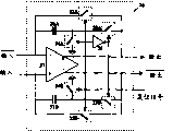
Figure 14 A and Figure 14 B illustrate the active integrator that is used to improve the output swing and the linearity respectively.At single-ended active integrator 29 shown in Figure 14 A.As connect, it comprises that a difference imports 35, one capacitors 31 of 30, one inverters of single-ended output amplifier and switch 32,33,34.Active integrator always remains virtual earth to the signal input, to eliminate the influence of condenser voltage to signal code.The bandwidth of amplifier 30 only need cover signal baseband needn't cover carrier wave, and this makes it is practicable.Inverter 35 utilizes reset signal as input, generate have delay the inverted reset signal with control switch 33, reset signal control switch 32 and 34 simultaneously.During reseting stage, switch 32 and 34 is connected, and switch 33 disconnects.The voltage of capacitor 31 resets to the input offset voltage of amplifier 30.During sampling phase, switch 32 and 34 disconnects and switch 33 connections.Capacitor 31 is charged by signal code.Simultaneously, offset the bias voltage of amplifier 30.At difference active integrator 36 shown in Figure 14 B.It comprises 37, two capacitor 31A of a differential-input differential output amplifier and 31B, inverter 35 and switch 32A, 32B, 33A, 33B, 34A, 34B.Except using differential input signal and providing the difference output, its working method is the same with integrator 29 basically.Integrator 29 can substitute the integrator 3 among Figure 1A, and the integrator 10 of integrator 36 in can alternate figures 3.
Figure 15 illustrates secondary BPCS circuit 38.It comprises 41, one the 2nd BPCS circuit 42 of 40, one amplifiers of 39, one chopper circuits of one the one BPCS circuit and a clock-signal generator 43 that produces second clock.The one BPCS circuit 39 and the 2nd BPCS circuit 42 can be any kinds in BPCS circuit 5,8,11,19,24 and 26.For a BPCS circuit 39, respectively two ends of a differential analog signal are offered its two inputs, and one first clock signal is imposed on its input end of clock.Produce some signal samplings and feed-in chopper circuit 40 from a BPCS circuit 39 with one first sampling rate.Under the control of second clock, symmetrically copped wave is carried out in these sampling on the time.From chopper circuit 40 copped wave with the new carrier frequency that equals chopping frequency after signal feed-in amplifier 41, and the differential signal after amplifying is fed to two inputs of the 2nd BPCS circuit 42 respectively.Under the control of second clock, the 2nd BPCS circuit 42 generates last sampling output with one second sampling rate.Secondary BPCS circuit 38 has provided the flexibility in the performance replacement.Can set up the more BPCS circuit of progression based on secondary BPCS circuit 38.
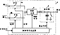
A kind of front end sampling radio receiver structure 44 shown in Figure 16.It comprises that has a f
Pass<2f
cLow pass filter, difference output low noise amplifier (LNA) 46, two BPCS circuit 47A and 47B, 90 ° of phase shifters 48, and a local oscillator 49.Be applied to the input of low pass filter 45 from the radio signal of antenna.2f
cAbove frequency component significantly reduces.The output feed-in LNA 46 of low pass filter 45 is to produce the enough big difference output of amplitude.Simultaneously difference output is fed to the input of BPCS circuit 47A and 47B.At the same time, the I clock signal feed-in BPCS circuit 47A of local oscillator 49 generations and the Q clock signal feed-in BPCS circuit 47B that behind 90 ° of phase shifters 48, generates from this I clock signal.BPCS circuit 47A and 47B produce I sampling and Q sampling respectively, and sampling output can or convert numerical data immediately to or is made for further processing.BPCS circuit 47A and 47B can be any among BPCS circuit 5,8,11,19,24 and 26.Integrator in these circuit can be passive integrator or can be active integrator.Radio receiver structure 44 has filtering, mixing and sampling function at front end simultaneously, and this has slowed down the performance requirement to the A/D conversion, has avoided analog filter and has highly used the DSP ability.In principle, any narrow bandwidth, promptly any high Q value is possible.Can easily compile and edit the centre frequency of filter function.This a kind of really super radio receiver structure that has broad field of application.
The capacitor that the sampling capacitor that uses in CS and BPCS circuit uses in than voltage sampling circuit is much bigger, thereby noise is low, electric charge is few and clock feedthrough is low.
The BPCS circuit is filter, frequency mixer and sampler simultaneously, thereby can work under radio frequency.Can pass through clock frequency, number n and W﹠amp; The wave setting centre frequency of S signal, bandwidth and adjacent selectivity, this is particularly useful for front end sampling radio receiver and system-on-a-chip.
Should understand, although set forth big measure feature of the present invention and characteristics and function detail of the present invention in this manual, this paper open only is exemplary and can makes various modifications in detail in the scope of the present invention that defines in following claims.
Claims (15)
1. band energising lotus sampling (BPCS) circuit (5) is characterized in that being used for controlling the control-signals generator (7) of first end and second end of differential analog signal, and this differential analog signal is at weighting and sampling (W﹠amp; S) during the stage response from the W﹠amp of described control-signals generator (7); The S signal is by W﹠amp; S element (6) is weighted, wherein only as described W﹠amp; The S signal is in W﹠amp; The electric current of S described analog signal during the stage is just by described W﹠amp; S element (6), and described control-signals generator (7) is applicable to that control will be at described W﹠amp; Carry out the described W﹠amp of integration during the S stage by integrator (3); The output signal of S element (6), wherein said W﹠amp; The electric current of the output signal of S element (6) is integrated into integral charge, in order at described W﹠amp; When finishing, the S stage generates ratio-voltage or electric current sampling at signal output part.
2. according to the band of claim 1 energising lotus sampling (BPCS) circuit (5), it is characterized in that: first switch (2A), this first switch (2A) have signal input part and the described weighting and the sampling (W﹠amp of first end that is used to receive described differential analog signal; S) signal output part that links to each other of the signal input part of element (6) and be connected so that control the control input end that this switch (2A) makes it only just to connect when receiving clock signal with the output terminal of clock of described control-signals generator (7); Second switch (2B), this second switch (2B) have signal input part and the described weighting and the sampling (W﹠amp of second end that is used to receive described differential analog signal; S) signal output part that connects of the described signal input part of element (6) and be connected in order to control the control input end that this switch (2B) makes it only just to connect when receiving clock signal with the reverse output terminal of clock of described control-signals generator (7); Described weighting and sampling (W﹠amp; S) element (7) has the W﹠amp with described control-signals generator; The control input end that the S signal output part connects is wherein only as described W﹠amp; The S signal is in the W﹠amp in the cycle that comprises n described clock; The electric current of S described analog signal during the stage is just by described W﹠amp; S element (6), and described W﹠amp; The S signal is controlled the electric current of described analog signal by constant, linearity, Gauss or other weighting function; And have and described W﹠amp; The integrator of the control input end that the signal input part that the output of S element (6) connects is connected with the reset signal output with described control-signals generator (7).
3. according to band energising lotus sampling (BPCS) circuit (5) of claim 1 or 2, it is characterized in that this control-signals generator (7) is applicable to this integrator of control, so that before the reseting stage of the described reset signal of beginning, keep sampling.
4. according to band energising lotus sampling (BPCS) circuit (5) of arbitrary claim among the claim 1-3, it is characterized in that the base-band content of described analog signal is represented in described sampling, and for 2 (p-1) f
c≤ f
In≤ pf
c, output frequency is f
Out=| f
In-(2p-1) f
c|, f wherein
InBe the frequency component of described analog signal, f
cBe the frequency of described clock, and p is 〉=1 integer, and the phase place of described output frequency depends on described f
InPhase place and described f
cPhase place, and p=1 definition basic frequency response range, and repeat identical waveform but amplitude reduces, and for given p, as (2p-1) f for p>1 frequency response
c-f
In1=f
In2-(2p-1) f
cThe time to frequency f
In1The f of (<(2p-1)
c) and f
In2The f of (>(2p-1)
c) obtain identical output frequency but the phase place difference, and the bandwidth of described frequency response and waveform depend on described n, and (n is big more, bandwidth is narrow more) and described weighting function (constant, linearity, Gauss or other function), described BPCS circuit is filter, frequency mixer and sampler simultaneously.
5. difference bandwidth electric charge sampling (BPCS) circuit (8), it is characterized in that the first and second BPCS circuit according to arbitrary claim among the claim 1-4, wherein the control-signals generator of all BPCS circuit is substituted by public control-signals generator (7), first signal input part of a described BPCS circuit is connected with first input end with second input of a described BPCS circuit respectively with the secondary signal input, and this first signal input part, the secondary signal input, the signal output part of the signal output part of a described BPCS circuit and described the 2nd BPCS circuit is first signal input part of described difference bandwidth electric charge sampling (BPCS) circuit, the secondary signal input, first signal output part and secondary signal output.
6. according to the difference band of claim 5 energising lotus sampling (BPCS) circuit (8), it is characterized in that, integrator (3A in a described BPCS circuit and described the 2nd BPCS circuit, 3B) be merged into an independent differential integrator (10), this differential integrator (10) is used for sampling to the difference current integration of described analog signal and in described first signal output part and the described secondary signal output generation difference of described difference BPCS circuit.
7. BPCS circuit in parallel (11) that comprises some BPCS circuit according to claim 1-4, it is characterized in that, all first signal input parts link together as first signal input part of described BPCS circuit in parallel, in order to receive first end of differential analog signal, all secondary signal inputs link together as the secondary signal input of described BPCS circuit in parallel, in order to receive second end of differential analog signal, discrete or the merging of all first switches, discrete or the merging of all second switches, and all control-signals generator in the described BPCS circuit are replaced by public control-signals generator (13), and multiplexer (11), this multiplexer (11) has the described some signal input parts that are connected with the signal output part of described BPCS circuit, the control input end that is connected with the multiplex signal output of described public control-signals generator, and signal output part, this multiplexer is used for during the stage output of described BPCS circuit being multiplexed to this signal output part when the output of the signal of described BPCS circuit is in maintenance, wherein this signal output part is the signal output part of described BPCS circuit in parallel, and described BPCS circuit in parallel improves sampling rate and two time intervals between the consecutive samples point are diminished, and should parallel connection BPCS circuit be single-ended.
8. BPCS circuit in parallel (11) that comprises some BPCS circuit according to claim 5 or 6, it is characterized in that, all first signal input parts link together as first signal input part of described BPCS circuit in parallel, in order to receive first end of differential analog signal, all secondary signal inputs link together as the secondary signal input of described BPCS circuit in parallel, in order to receive second end of differential analog signal, discrete or the merging of all first switches in the described BPCS circuit, discrete or the merging of all second switches in the described BPCS circuit, discrete or the merging of all first switches in described the 2nd BPCS circuit, discrete or the merging of all second switches in described the 2nd BPCS circuit, all control-signals generator in the described BPCS circuit are replaced by public control-signals generator, and multiplexer, this multiplexer has right to the described some signal input parts that are connected with the signal output part of described BPCS circuit, the control input end that is connected with the multiplex signal output of described public control-signals generator, and pair of output, this multiplexer be used for when the output of the signal of described BPCS circuit during the stage that the output of described BPCS circuit is right to being multiplexed to this signal output part to being in maintenance, wherein this signal output part is to being that the signal output part of described BPCS circuit in parallel is right, and described BPCS circuit in parallel improves sampling rate and two time intervals between the consecutive samples point are diminished, and should parallel connection BPCS circuit be difference type wherein.
9. a BPCS circuit in parallel that comprises some BPCS circuit according to claim 7 or 8 is characterized in that control-signals generator, and this control-signals generator has input end of clock, output terminal of clock, oppositely output terminal of clock, described some W﹠amp; S signal output part, described some reset signal outputs and described some multiplex signal outputs, wherein input end of clock is the input end of clock of described BPCS circuit in parallel, be used for generating clock signal at the output terminal of clock place of the described global semaphore control generator that is connected with the control input end of all first switches of described BPCS circuit, and be used for generating reverse clock, described some W﹠amp at the reverse output terminal of clock place that is connected with the control input end of all second switches of described BPCS circuit; All W﹠amp of S signal output part and described BPCS circuit; The control input end of S element (9A-9X) connects, the control input end of all integrators (10A-10X) of described some reset signal outputs and described BPCS circuit is connected, and described some multiplex signals, reset signal, sampled signal and multiplex signal distance when being even.
10. one kind comprises according to the secondary BPCS circuit of the first and second BPCS circuit (39,42) of the claim 1-6 of front or the arbitrary claim among the 7-9, it is characterized in that:
First signal input part and secondary signal input, be used for receiving at a described BPCS circuit (39) respectively first end and second end of differential analog signal, so that produce signal sampling to sentencing first sampling rate at the signal output part or the signal output part of a described BPCS circuit;
Chopper circuit (40) is used for signal output part or the clock signal frequency of output to locating to equate according to described first sampling rate at it, in time symmetrically to signal copped wave from a BPCS circuit (39),
Difference output amplifier (41) is used for amplifying signal from this chopper circuit at its signal output part to locating difference ground; And
The signal output part of first signal input part of described the 2nd BPCS and secondary signal input and described amplifier (41) is to being connected, in order to produce signal sampling to locating according to second sampling rate at signal output part or output.
11. secondary BPCS circuit according to claim 10, it is characterized in that having the clock generator (43) of input end of clock, be used for receiving first clock signal of using by a BPCS circuit (39), and be used to generate the second clock signal of the input end of clock of the input end of clock of the described chopper circuit of feed-in simultaneously and described the 2nd BPCS circuit.
12. the configuration of the cordwood system type in any described BPCS circuit of foundation claim 1-11 is characterized in that:
The n-MOS of described switch configuration comprises: the n-MOS transistor, it drains as signal input part, grid as the control input end and source electrode as signal output part; And
The CMOS configuration of described switch comprises: n-MOS transistor and p-MOS transistor, and their drain electrode is connected to each other as signal input part, and their source electrode is connected to each other as signal output part, and the transistorized grid of described n-MOS is as the control input end; Inverter, its input are connected with the transistorized grid of described n-MOS and its output is connected with the transistorized grid of described p-MOS;
Described W﹠amp; The configuration of S element comprises: the n-MOS transistor, it drains as signal input part, grid as the control input end and source electrode as signal output part;
The passive type configuration of described integrator, comprising: its first end is as the capacitor of the signal input part and the second end ground connection; Be inserted in the resistor of selecting for use between first end of described signal input part and described capacitor when needed; The n-MOS transistor, its drain electrode is connected with second end with first end of described capacitor respectively with source electrode, and grid is as the control input end;
The configuration of the passive type of described differential integrator comprises: first passive configuration of described integrator, its signal input part and signal output part are respectively as first signal input part and first signal output part of described differential integrator; And second passive configuration of described integrator, its signal input part and signal output part are respectively as the secondary signal input and the secondary signal output of described differential integrator;
The active formula configuration of described integrator, comprising: difference is imported single-ended output amplifier, its positive input terminal ground connection, negative input end is as the signal input part of described integrator, and its output is as the signal output part of described integrator; Its first end and described difference are imported the capacitor that the negative input end of single-ended output amplifier is connected; Its input is as the inverter of the control input end of described integrator; The one n-MOS configuration of described switch or CMOS configuration, its signal input part is connected with the negative input end that described difference is imported single-ended output amplifier, the control input end of control input end and described integrator is connected, and signal output part is connected with the output that described difference is imported single-ended output amplifier; The 2nd n-MOS configuration of described switch or CMOS configuration, second end of its signal input part and described capacitor is connected, and the control input end of control input end and described integrator is connected, and signal output part ground connection; The 3rd n-MOS of described switch configuration or CMOS configuration, second end of its signal input part and described capacitor is connected, and the output of control input end and described inverter is connected and signal output part is connected with the output that described difference is imported single-ended output amplifier; And be inserted in the resistor of selecting for use between the signal input part of described integrator and the negative input end that described difference is imported single-ended output amplifier when needed;
The active formula configuration of described differential integrator, comprise: differential-input differential output amplifier, its negative input end, positive input terminal, positive output end and negative output terminal are first signal input part, secondary signal input, first signal output part and the secondary signal outputs of described differential integrator; First capacitor, the negative input end of its first end and described differential-input differential output amplifier is connected; Second capacitor, the positive input terminal of its first end and described differential-input differential output amplifier is connected; Inverter, its input is as the control input end of described differential integrator; The one n-MOS configuration of described switch or CMOS configuration, its signal input part is connected with the negative input end of described differential-input differential output amplifier, and the control input end of control input end and described differential integrator is connected and the positive output end of signal output part and described differential-input differential output amplifier is connected; The 2nd n-MOS configuration of described switch or CMOS configuration, second end of its signal input part and described first capacitor is connected, and the control input end of control input end and described differential integrator is connected and signal output part ground connection; The 3rd n-MOS configuration of described switch or CMOS configuration, second end of its signal input part and described first capacitor is connected, and the output of control input end and described inverter is connected and the positive output end of signal output part and described differential-input differential output amplifier is connected; The 4th n-MOS configuration of described switch or CMOS configuration, its signal input part is connected with the positive input terminal of described differential-input differential output amplifier, and the control input end of control input end and described differential integrator is connected and the negative output terminal of signal output part and described differential-input differential output amplifier is connected; The 5th n-MOS configuration of described switch or CMOS configuration, second end of its signal input part and described second capacitor is connected, and the control input end of control input end and described differential integrator is connected and signal output part ground connection; The 6th n-MOS configuration of described switch or CMOS configuration, second end of its signal input part and described second capacitor is connected, and the output of control input end and described inverter is connected and the negative output terminal of signal output part and described differential-input differential output amplifier is connected; When needing, be inserted in first between the negative input end of first signal input part of described differential integrator and described differential-input differential output amplifier and select resistor for use; And when needing, be inserted in second between the positive input terminal of the secondary signal input of described differential integrator and described differential-input differential output amplifier and select resistor for use.
13. one kind comprises according to the front end sampling radio receiver arrangement of the first and second BPCS circuit of claim 1-11, it is characterized in that comprising:
Bandwidth up to two times of clock frequency, be used to receive and the low pass filter (45) of filtering radio signal;
Be used for producing the low noise amplifier (46) of the radio signal of difference amplification from this signal through filtering;
Be used for producing the local oscillator (49) of I clock signal at its signal output part;
The pi/2 phase shifter (48) that its signal input part is connected with local oscillator (49) is used for equating but the Q clock signal of phase difference pi/2 with respect to described I clock signal amplitude in its signal output part place generation;
Two right ends of the signal output part of described low noise amplifier (46) all are connected to a BPCS circuit (47A) and the 2nd BPCS circuit (47B), described I clock signal output terminal is connected with the input end of clock of a described BPCS circuit (47A), and described Q clock signal output terminal is connected with the input end of clock of described the 2nd BPCS circuit (47B), be used for the signal output part of a described BPCS circuit (47A) or output to the baseband I sampling of locating to produce described radio signal and at the signal output part of described the 2nd BPCS circuit (47B) or output to locating to produce the base band Q sampling of described radio signal.
14. the front end sampling radio receiver arrangement according to claim 13 is characterized in that:
Described local oscillator (49), described phase shifter (48) and the described first and second BPCS circuit (47A, clock generator 47B) is combined so that more effectively and more accurately produce difference I clock signal and Q clock signal;
Described baseband I sampling and Q sampling are changed by two discrete A/D converters or single A/D converter, so that be multiplexed into digital signal;
Described digital signal is handled by Digital Signal Processing (DSP) parts; And
Described front end sampling radio receiver arrangement is a kind of advanced wireless electricity receiver device of simplifying the simulation part greatly and wherein highly utilizing the DSP ability.
15. an electric charge methods of sampling is characterized in that following step: at W﹠amp; During the S stage to the first and second end weightings of differential analog signal, at described W﹠amp; Signal during the S stage behind the integral weighting, wherein the electric current of the signal after this weighting is integrated into integral charge; And
At described W﹠amp; When finishing, produces ratio-voltage or electric current sampling in the S stage.
Applications Claiming Priority (2)
| Application Number | Priority Date | Filing Date | Title |
|---|---|---|---|
| SE99035321 | 1999-09-28 | ||
| SE9903532A SE9903532D0 (en) | 1999-09-28 | 1999-09-28 | Versatile charge sampling circuits |
Related Parent Applications (1)
| Application Number | Title | Priority Date | Filing Date |
|---|---|---|---|
| CNB008135592A Division CN1174431C (en) | 1999-09-28 | 2000-09-25 | Versatile charge sampling circuits |
Publications (1)
| Publication Number | Publication Date |
|---|---|
| CN1551505A true CN1551505A (en) | 2004-12-01 |
Family
ID=20417207
Family Applications (2)
| Application Number | Title | Priority Date | Filing Date |
|---|---|---|---|
| CNA2004100598399A Pending CN1551505A (en) | 1999-09-28 | 2000-09-25 | Versatile charge sampling circuits |
| CNB008135592A Expired - Fee Related CN1174431C (en) | 1999-09-28 | 2000-09-25 | Versatile charge sampling circuits |
Family Applications After (1)
| Application Number | Title | Priority Date | Filing Date |
|---|---|---|---|
| CNB008135592A Expired - Fee Related CN1174431C (en) | 1999-09-28 | 2000-09-25 | Versatile charge sampling circuits |
Country Status (9)
| Country | Link |
|---|---|
| US (3) | US7053673B1 (en) |
| EP (2) | EP2228800A3 (en) |
| JP (2) | JP4685310B2 (en) |
| CN (2) | CN1551505A (en) |
| AT (1) | ATE506677T1 (en) |
| AU (1) | AU7820100A (en) |
| DE (1) | DE60045867D1 (en) |
| SE (1) | SE9903532D0 (en) |
| WO (1) | WO2001024192A1 (en) |
Families Citing this family (17)
| Publication number | Priority date | Publication date | Assignee | Title |
|---|---|---|---|---|
| WO2005031755A1 (en) * | 2003-09-29 | 2005-04-07 | Nokia Corporation | Active current mode sampling circuit |
| JP5046622B2 (en) | 2005-12-13 | 2012-10-10 | パナソニック株式会社 | Sampling filter device |
| US7671658B2 (en) | 2006-05-24 | 2010-03-02 | Panasonic Corporation | Mixer having frequency selection function |
| JP5258559B2 (en) * | 2006-06-08 | 2013-08-07 | パナソニック株式会社 | Discrete filter, sampling mixer and radio apparatus |
| JP2008017220A (en) * | 2006-07-06 | 2008-01-24 | Sony Corp | Charged main filter circuit |
| WO2008050630A1 (en) | 2006-10-23 | 2008-05-02 | Panasonic Corporation | Sampling filter device and radio communication device |
| FR2911449B1 (en) * | 2007-01-16 | 2009-02-27 | Commissariat Energie Atomique | SAMPLE FILTER WITH FINITE IMPULSE RESPONSE |
| US8385874B2 (en) | 2007-03-06 | 2013-02-26 | Panasonic Corporation | Discrete time direct sampling circuit and receiver |
| WO2008142486A1 (en) * | 2007-05-18 | 2008-11-27 | Nokia Corporation | Analogue-to-digital converter |
| WO2009090883A1 (en) * | 2008-01-16 | 2009-07-23 | Panasonic Corporation | Sampling filter device |
| EP2483891A2 (en) * | 2009-09-28 | 2012-08-08 | Arctic Silicon Devices As | Input configuration for analog to digital converter |
| FR2954628B1 (en) * | 2009-12-18 | 2012-02-24 | Commissariat Energie Atomique | DEVICE AND METHOD FOR RECEIVING RF SIGNALS BASED ON A HETERODYNE ARCHITECTURE WITH UNDER-SAMPLING COMPLEX IF |
| US9287851B2 (en) | 2011-03-22 | 2016-03-15 | Ess Technology, Inc. | Finite impulse response filter for producing outputs having different phases |
| WO2012129271A1 (en) * | 2011-03-22 | 2012-09-27 | Ess Technology, Inc. | Finite impulse response filter for producing outputs having different phases |
| ITFO20110009A1 (en) * | 2011-08-12 | 2013-02-13 | Marco Bennati | SYSTEM AND METHOD OF REDUCTION OF NOISE IN CHAMPIONSHIP AMPLIFIERS. |
| US20140049291A1 (en) | 2012-08-14 | 2014-02-20 | Luxen Technologies, Inc. | Noise-resistant sampling circuit and image sensor |
| CN107918443B (en) * | 2016-10-11 | 2020-04-24 | 深圳市中兴微电子技术有限公司 | Signal generation method and device |
Family Cites Families (30)
| Publication number | Priority date | Publication date | Assignee | Title |
|---|---|---|---|---|
| IT1186340B (en) * | 1985-10-29 | 1987-11-26 | Sgs Microelettronica Spa | DIFFERENTIAL INTEGRATOR WITH SWITCHED CONDENSER USING A SINGLE INTEGRATION CONDENSER |
| JPS62145927A (en) * | 1985-12-20 | 1987-06-30 | Hitachi Ltd | Data converter |
| IT1227615B (en) * | 1988-12-22 | 1991-04-22 | Sgs Thomson Microelectronics | FILTER COMPLETELY DIFFERENTIAL WITH SWITCHED CAPACITORS USING OPERATIONAL AMPLIFIERS CMOS WITHOUT COMMON MODE FEEDBACK |
| US5128966A (en) * | 1989-02-15 | 1992-07-07 | Samsung Electronics Co., Ltd. | System for demodulating frequency- or phase-modulated signals by quadrature-phase |
| US5162670A (en) * | 1990-01-26 | 1992-11-10 | Kabushiki Kaisha Toshiba | Sample-and-hold circuit device |
| JP3337241B2 (en) * | 1991-07-26 | 2002-10-21 | テキサス インスツルメンツ インコーポレイテツド | Improved multi-channel sensor interface circuit and manufacturing method thereof |
| JPH06236698A (en) * | 1993-02-10 | 1994-08-23 | Tamagawa Seiki Co Ltd | Sample-hold method and circuit of sine wave |
| EP0620442B1 (en) * | 1993-04-08 | 2001-07-25 | Lecroy S.A. | Charge sampling circuit |
| US5414311A (en) | 1993-09-14 | 1995-05-09 | Carnegie Mellon University | Sample and hold circuit and finite impulse response filter constructed therefrom |
| US5392043A (en) * | 1993-10-04 | 1995-02-21 | General Electric Company | Double-rate sampled signal integrator |
| US5617093A (en) * | 1994-09-30 | 1997-04-01 | Imp, Inc. | Switched capacitor analog circuits with low input capacitance |
| JP2708007B2 (en) * | 1995-03-31 | 1998-02-04 | 日本電気株式会社 | Sample and hold circuit |
| JPH0983588A (en) * | 1995-09-18 | 1997-03-28 | Mitsubishi Electric Corp | Demodulator modulation/demodulation system and demodulation method |
| US5617063A (en) * | 1995-12-13 | 1997-04-01 | Pacific Communication Sciences, Inc. | Matched filters for processing related signal components |
| JP3392670B2 (en) * | 1996-11-28 | 2003-03-31 | 株式会社東芝 | Sampling device |
| EP0863606B1 (en) * | 1997-03-05 | 2003-09-24 | Nec Corporation | Direct conversion receiver capable of cancelling DC offset voltages |
| JPH1127569A (en) * | 1997-07-01 | 1999-01-29 | Fuji Film Micro Device Kk | Signal-sampling device |
| US5982315A (en) * | 1997-09-12 | 1999-11-09 | Qualcomm Incorporated | Multi-loop Σ Δ analog to digital converter |
| US6320459B2 (en) * | 1997-11-24 | 2001-11-20 | Mccullough Rob | Notch filter implemented using analog sampling |
| US6243430B1 (en) * | 1998-01-09 | 2001-06-05 | Qualcomm Incorporated | Noise cancellation circuit in a quadrature downconverter |
| JPH11234150A (en) * | 1998-02-09 | 1999-08-27 | Toshiba Corp | Digital demodulator |
| FI120124B (en) * | 1998-05-29 | 2009-06-30 | Nokia Corp | A method and circuit for sampling a signal at a high sampling rate |
| US6181748B1 (en) * | 1998-07-07 | 2001-01-30 | Macronix International Co. | Pulse shaper apparatus and method for ISDN U-interface |
| JP3568102B2 (en) * | 1998-07-24 | 2004-09-22 | 松下電器産業株式会社 | Direct conversion receiver |
| US6157331A (en) * | 1998-10-01 | 2000-12-05 | Tritech Microelectronics, Ltd. | Sigma delta modulator with automatic saturation detection and recovery |
| US6246867B1 (en) * | 1998-11-17 | 2001-06-12 | Telefonaktiebolaget Lm Ericsson (Publ) | Method and apparatus for saving current while performing signal strength measurements in a homodyne receiver |
| US6366622B1 (en) * | 1998-12-18 | 2002-04-02 | Silicon Wave, Inc. | Apparatus and method for wireless communications |
| US6757340B1 (en) * | 1999-02-22 | 2004-06-29 | Telefonaktiebolaget L M Ericsson (Publ) | Radio receiver and method for preloading an average DC-offset into a channel filter |
| US6201835B1 (en) * | 1999-03-05 | 2001-03-13 | Burr-Brown Corporation | Frequency-shaped pseudo-random chopper stabilization circuit and method for delta-sigma modulator |
| US6943618B1 (en) * | 1999-05-13 | 2005-09-13 | Honeywell International Inc. | Compensation mechanism for compensating bias levels of an operation circuit in response to supply voltage changes |
-
1999
- 1999-09-28 SE SE9903532A patent/SE9903532D0/en unknown
-
2000
- 2000-09-25 EP EP10168098A patent/EP2228800A3/en not_active Withdrawn
- 2000-09-25 EP EP00968260A patent/EP1221166B1/en not_active Expired - Lifetime
- 2000-09-25 JP JP2001527292A patent/JP4685310B2/en not_active Expired - Fee Related
- 2000-09-25 CN CNA2004100598399A patent/CN1551505A/en active Pending
- 2000-09-25 AT AT00968260T patent/ATE506677T1/en not_active IP Right Cessation
- 2000-09-25 CN CNB008135592A patent/CN1174431C/en not_active Expired - Fee Related
- 2000-09-25 DE DE60045867T patent/DE60045867D1/en not_active Expired - Lifetime
- 2000-09-25 AU AU78201/00A patent/AU7820100A/en not_active Abandoned
- 2000-09-25 WO PCT/SE2000/001854 patent/WO2001024192A1/en active Application Filing
- 2000-09-28 US US09/672,803 patent/US7053673B1/en not_active Expired - Fee Related
-
2005
- 2005-04-06 US US11/099,460 patent/US8035421B2/en not_active Expired - Fee Related
- 2005-04-06 US US11/099,488 patent/US7023245B2/en not_active Expired - Fee Related
-
2010
- 2010-12-09 JP JP2010274877A patent/JP4875201B2/en not_active Expired - Fee Related
Also Published As
| Publication number | Publication date |
|---|---|
| JP4875201B2 (en) | 2012-02-15 |
| DE60045867D1 (en) | 2011-06-01 |
| US8035421B2 (en) | 2011-10-11 |
| CN1377504A (en) | 2002-10-30 |
| JP2011103666A (en) | 2011-05-26 |
| WO2001024192A1 (en) | 2001-04-05 |
| EP1221166A1 (en) | 2002-07-10 |
| EP2228800A3 (en) | 2010-09-29 |
| AU7820100A (en) | 2001-04-30 |
| US20050168371A1 (en) | 2005-08-04 |
| SE9903532D0 (en) | 1999-09-28 |
| JP2003510933A (en) | 2003-03-18 |
| JP4685310B2 (en) | 2011-05-18 |
| EP2228800A2 (en) | 2010-09-15 |
| US7023245B2 (en) | 2006-04-04 |
| CN1174431C (en) | 2004-11-03 |
| US20050176397A1 (en) | 2005-08-11 |
| ATE506677T1 (en) | 2011-05-15 |
| US7053673B1 (en) | 2006-05-30 |
| EP1221166B1 (en) | 2011-04-20 |
Similar Documents
| Publication | Publication Date | Title |
|---|---|---|
| CN1174431C (en) | Versatile charge sampling circuits | |
| US7068203B2 (en) | Switched-capacitor circuits with reduced finite-gain effect | |
| Ranganathan et al. | Discrete-time parametric amplification based on a three-terminal MOS varactor: Analysis and experimental results | |
| CN200994116Y (en) | Current feedback differential amplifying-sampling circuit and air conditioner with same | |
| CN104767525A (en) | Analog-to-digital converter and image sensor | |
| US20230095702A1 (en) | Method for eliminating multi-channel gain errors of eeg signal acquisition system | |
| CN105871376A (en) | Voltage sampling and driver amplifier flicker noise cancellation in a switched capacitor analog-to-digital converter | |
| CN105676263B (en) | A kind of pulse signal peak-value detection method based on phase compensation | |
| CN110798212B (en) | Time domain interleaved waveform synthesis timing mismatch calibration device and method | |
| CN101764588A (en) | Filter circuit and communication device | |
| CN103580691A (en) | Assembly line ADC sublevel circuit for dynamically compensating offset error and capacitance mismatch error | |
| CN102017410B (en) | Switched-capacitor decimator | |
| CN111555727A (en) | High-gain low-noise switched capacitor adjustable gain amplifier | |
| CN100438341C (en) | Pipelined analog-to-digital converter | |
| CN1853341A (en) | Mixer circuit, receiver comprising a mixer circuit, method for generating an output signal by mixing an input signal with an oscillator signal | |
| CN114614843A (en) | DCOC circuit for zero intermediate frequency receiver | |
| CN102714502B (en) | A/D change-over circuit | |
| US20020172170A1 (en) | Spread spectrum demodulation using a subsampling communication receiver architecture | |
| CN101789789B (en) | Generating circuit from reference voltage | |
| WO2018039674A1 (en) | Wake up receiver using multiphase peak detector and demodulator | |
| CN102299699A (en) | signal filter, filtering method and signal monitoring system | |
| Palagiri et al. | Performance analysis of first order digital sigma delta ADC | |
| CN101340196B (en) | Multichannel digital detection IF amplifier | |
| Thomas et al. | A 1-to-4 SiGe BiCMOS analog demultiplexer sampling front-end for a 116 GBaud-receiver | |
| Yim et al. | A 200-MHz CMOS I/Q downconverter |
Legal Events
| Date | Code | Title | Description |
|---|---|---|---|
| C06 | Publication | ||
| PB01 | Publication | ||
| C10 | Entry into substantive examination | ||
| SE01 | Entry into force of request for substantive examination | ||
| C02 | Deemed withdrawal of patent application after publication (patent law 2001) | ||
| WD01 | Invention patent application deemed withdrawn after publication |