JP4875201B2 - Various charge sampling circuits - Google Patents
Various charge sampling circuits Download PDFInfo
- Publication number
- JP4875201B2 JP4875201B2 JP2010274877A JP2010274877A JP4875201B2 JP 4875201 B2 JP4875201 B2 JP 4875201B2 JP 2010274877 A JP2010274877 A JP 2010274877A JP 2010274877 A JP2010274877 A JP 2010274877A JP 4875201 B2 JP4875201 B2 JP 4875201B2
- Authority
- JP
- Japan
- Prior art keywords
- signal
- input
- output
- bpcs
- circuit
- Prior art date
- Legal status (The legal status is an assumption and is not a legal conclusion. Google has not performed a legal analysis and makes no representation as to the accuracy of the status listed.)
- Expired - Fee Related
Links
- 238000005070 sampling Methods 0.000 title claims abstract description 129
- 230000018199 S phase Effects 0.000 claims abstract description 6
- 230000004044 response Effects 0.000 claims description 44
- 239000003990 capacitor Substances 0.000 claims description 34
- 238000000034 method Methods 0.000 claims description 12
- 230000007423 decrease Effects 0.000 claims description 6
- 238000001914 filtration Methods 0.000 claims description 6
- 238000010586 diagram Methods 0.000 description 12
- 230000008569 process Effects 0.000 description 6
- 238000004088 simulation Methods 0.000 description 6
- 238000006243 chemical reaction Methods 0.000 description 4
- 230000008901 benefit Effects 0.000 description 2
- 230000000694 effects Effects 0.000 description 2
- 230000010354 integration Effects 0.000 description 2
- 230000002238 attenuated effect Effects 0.000 description 1
- 230000008859 change Effects 0.000 description 1
Images


Classifications
-
- H—ELECTRICITY
- H04—ELECTRIC COMMUNICATION TECHNIQUE
- H04B—TRANSMISSION
- H04B1/00—Details of transmission systems, not covered by a single one of groups H04B3/00 - H04B13/00; Details of transmission systems not characterised by the medium used for transmission
- H04B1/0003—Software-defined radio [SDR] systems, i.e. systems wherein components typically implemented in hardware, e.g. filters or modulators/demodulators, are implented using software, e.g. by involving an AD or DA conversion stage such that at least part of the signal processing is performed in the digital domain
- H04B1/0007—Software-defined radio [SDR] systems, i.e. systems wherein components typically implemented in hardware, e.g. filters or modulators/demodulators, are implented using software, e.g. by involving an AD or DA conversion stage such that at least part of the signal processing is performed in the digital domain wherein the AD/DA conversion occurs at radiofrequency or intermediate frequency stage
-
- G—PHYSICS
- G11—INFORMATION STORAGE
- G11C—STATIC STORES
- G11C27/00—Electric analogue stores, e.g. for storing instantaneous values
- G11C27/02—Sample-and-hold arrangements
- G11C27/024—Sample-and-hold arrangements using a capacitive memory element
-
- H—ELECTRICITY
- H04—ELECTRIC COMMUNICATION TECHNIQUE
- H04B—TRANSMISSION
- H04B1/00—Details of transmission systems, not covered by a single one of groups H04B3/00 - H04B13/00; Details of transmission systems not characterised by the medium used for transmission
-
- H—ELECTRICITY
- H04—ELECTRIC COMMUNICATION TECHNIQUE
- H04B—TRANSMISSION
- H04B1/00—Details of transmission systems, not covered by a single one of groups H04B3/00 - H04B13/00; Details of transmission systems not characterised by the medium used for transmission
- H04B1/06—Receivers
- H04B1/16—Circuits
- H04B1/26—Circuits for superheterodyne receivers
- H04B1/28—Circuits for superheterodyne receivers the receiver comprising at least one semiconductor device having three or more electrodes
Landscapes
- Engineering & Computer Science (AREA)
- Computer Networks & Wireless Communication (AREA)
- Signal Processing (AREA)
- Analogue/Digital Conversion (AREA)
- Networks Using Active Elements (AREA)
- Peptides Or Proteins (AREA)
- Separation By Low-Temperature Treatments (AREA)
- Transition And Organic Metals Composition Catalysts For Addition Polymerization (AREA)
- Glass Compositions (AREA)
Abstract
Description
現在、アナログ・ディジタル(A/D)変換には電圧サンプリングが用いられている。電圧サンプラには、信号源とコンデンサとの間にサンプリング・スイッチが設けられている。2つのサンプリング時刻の間、コンデンサ電圧は信号電圧を正確に追跡する。サンプリング時刻にスイッチを切ってコンデンサ電圧を保持する。信号の周波数が増加すると、この2つのプロセスは非常に困難になる。所定の精度では、熱雑音とスイッチング雑音によって最小許容容量が規定され、追跡速度によって最大許容容量またはスイッチ抵抗が規定される。この最大が最小より小さいと不可能になる。また、クロックのジターと有限のターンオフ速度(非ゼロのサンプリング隙間)のためにサンプリングのタイミングが不正確になる。実際のところ、電圧サンプリング回路の帯域幅は信号の帯域幅よりかなり大きくなければならない。このため、高周波無線信号を直接サンプリングすることが非常に困難である。サブサンプリングを行えばサンプリング速度は減少するが、サンプリング回路の帯域幅は減少しないし、クロックのジターを小さくしまたサンプリング隙間を小さくしたいという要求も減らない。 Currently, voltage sampling is used for analog-to-digital (A / D) conversion. The voltage sampler is provided with a sampling switch between the signal source and the capacitor. During the two sampling times, the capacitor voltage accurately tracks the signal voltage. Switch off the sampling time to hold the capacitor voltage. As the frequency of the signal increases, the two processes become very difficult. For a given accuracy, the minimum allowable capacitance is defined by thermal noise and switching noise, and the maximum allowable capacitance or switch resistance is defined by tracking speed. It becomes impossible if this maximum is less than the minimum. Also, sampling timing is inaccurate due to clock jitter and finite turn-off speed (non-zero sampling gap). In practice, the bandwidth of the voltage sampling circuit must be much larger than the bandwidth of the signal. For this reason, it is very difficult to directly sample high-frequency radio signals. Sub-sampling reduces the sampling speed, but does not reduce the bandwidth of the sampling circuit, and does not reduce the demand to reduce clock jitter and the sampling gap.
本発明の目的は、上に述べた問題を解決するための改善されたサンプリング回路とアナログ信号のサンプリング方法を提供することである。 It is an object of the present invention to provide an improved sampling circuit and analog signal sampling method for solving the above-mentioned problems.
前記目的を達成する本発明の電荷サンプリング(CS)回路は制御信号発生器を備え、サンプリング段階で制御信号発生器からのサンプリング信号に応じて電荷サンプリング回路へのアナログ入力信号を制御して積分器で積分する。すなわち、アナログ入力信号の電流を積分して積分電荷を生成して、サンプリング段階の終わりに比例電圧または電流サンプルを信号出力に生成する。 The charge sampling (CS) circuit of the present invention that achieves the above object includes a control signal generator, and controls an analog input signal to the charge sampling circuit in accordance with a sampling signal from the control signal generator in a sampling stage. Integrate with. That is, the current of the analog input signal is integrated to generate an integrated charge, and a proportional voltage or current sample is generated at the signal output at the end of the sampling phase.
本発明の更に特定の目的は、帯域通過サンプリングのための方法とサンプリング回路を提供することである。 A more specific object of the invention is to provide a method and sampling circuit for bandpass sampling.
この目的を達成する帯域通過サンプリング(BPCS)回路は制御信号発生器を備え、重みおよびサンプリング(weighting-and-sampling)(W&S)段階で制御信号発生器からのW&S信号に応じて、差動アナログ信号の第1の端と第2の端を制御してW&S要素で重みを付ける。この場合、前記W&S信号がW&S段階にあるときだけアナログ信号の電流は前記W&S要素を通過し、前記制御信号発生器はW&S段階でW&S要素の出力信号を制御して積分器で積分する。すなわち、W&S要素の出力信号の電流を積分して積分電荷を生成して、W&S段階の終わりに比例電圧または電流サンプルを信号出力に生成する。 A band-pass sampling (BPCS) circuit that achieves this objective includes a control signal generator, and in the weighting-and-sampling (W & S) stage, a differential analog signal is generated according to the W & S signal from the control signal generator. The first and second ends of the signal are controlled and weighted with a W & S element. In this case, only when the W & S signal is in the W & S stage, the current of the analog signal passes through the W & S element, and the control signal generator controls the output signal of the W & S element in the W & S stage and integrates it with an integrator. That is, the current in the output signal of the W & S element is integrated to generate an integrated charge, and a proportional voltage or current sample is generated at the signal output at the end of the W & S phase.
本発明の別の特定の目的は、2ステップBPCS回路を提供することである。これを達成する本発明の2ステップBPCS回路は、第1のサンプリング速度で信号サンプルを生成する本発明の第1のBPCS回路と、第1のサンプリング速度に等しいクロック信号の周波数で時間的に対称に第1のBPCS回路からの信号をその信号出力または出力対でチョッピングするチョッピング回路と、チョッピング回路からの信号を差動的に増幅する差動出力増幅器とを備える。ここで、前記第2のBPCSの第1の信号入力と第2の信号入力は前記増幅器(41)の信号出力対に接続して、信号サンプルを第2のサンプリング速度で信号出力または出力対に生成する。 Another particular object of the present invention is to provide a two-step BPCS circuit. The two-step BPCS circuit of the present invention that achieves this is symmetric in time with the frequency of the clock signal equal to the first sampling rate, with the first BPCS circuit of the present invention that generates signal samples at the first sampling rate. And a chopping circuit for chopping a signal from the first BPCS circuit by its signal output or output pair, and a differential output amplifier for differentially amplifying the signal from the chopping circuit. Here, the first signal input and the second signal input of the second BPCS are connected to the signal output pair of the amplifier (41), and the signal sample is output to the signal output or output pair at the second sampling rate. Generate.
本発明の更に別の特定の目的は、フロントエンド・サンプリング無線受信機を提供することである。これを達成する本発明のフロントエンド・サンプリング無線受信機は、クロック周波数の2倍以下の帯域幅で無線信号を受信して濾波する低域フィルタと、濾波された信号から差動的に増幅された無線信号を生成する低雑音増幅器と、Iクロック信号をその信号出力に生成するローカル発振器と、ローカル発振器に接続する信号入力を有してIクロック信号に対して振幅は同じで位相はπ/2シフトしたQクロック信号をその信号出力に生成するπ/2位相シフタとを備える。ここで、前記低雑音増幅器の信号出力対の2端を第1のBPCS回路と第2のBPCS回路にそれぞれ接続し、前記Iクロック信号出力を前記第1のBPCS回路のクロック入力に接続し、Qクロック信号出力を第2のBPCS回路のクロック入力に接続して、無線信号のベースバンドIサンプルを第1のBPCS回路の信号出力または出力対に生成し、無線信号のベースバンドQサンプルを前記第2のBPCS回路の信号出力または出力対に生成する。 Yet another specific object of the present invention is to provide a front-end sampling radio receiver. To achieve this, the front-end sampling radio receiver of the present invention includes a low-pass filter that receives and filters a radio signal with a bandwidth that is less than twice the clock frequency, and a differentially amplified signal from the filtered signal. A low noise amplifier for generating a radio signal, a local oscillator for generating an I clock signal at its signal output, and a signal input connected to the local oscillator, the amplitude of which is the same as that of the I clock signal, and the phase is π / A π / 2 phase shifter for generating a Q-shift signal shifted by 2 at its signal output. Here, two ends of the signal output pair of the low noise amplifier are respectively connected to a first BPCS circuit and a second BPCS circuit, and the I clock signal output is connected to a clock input of the first BPCS circuit, The Q clock signal output is connected to the clock input of the second BPCS circuit to generate a baseband I sample of the radio signal to the signal output or output pair of the first BPCS circuit, and the baseband Q sample of the radio signal is The second BPCS circuit generates a signal output or output pair.
本発明に係る電荷サンプリング回路の利点は、電荷サンプリング回路の帯域幅を信号の帯域幅より非常に大きくする必要がないことである。別の重要な背景は、無線信号では、搬送波周波数がいかに高くても、信号帯域幅(ベースバンド)はDCと搬送波周波数の間の全帯域のごく小部分である、ということである。したがって全帯域を変換する必要がなく、信号を持つ帯域だけでよい。 An advantage of the charge sampling circuit according to the present invention is that the bandwidth of the charge sampling circuit need not be much larger than the signal bandwidth. Another important background is that for wireless signals, no matter how high the carrier frequency, the signal bandwidth (baseband) is a small fraction of the entire band between DC and the carrier frequency. Therefore, it is not necessary to convert the entire band, and only a band having a signal is required.
所定の精度において、CS回路またはBPCS回路でサンプリングする信号の周波数は電圧サンプリング回路の周波数より幾分高いかまたは非常に高い。 At a given accuracy, the frequency of the signal sampled by the CS circuit or the BPCS circuit is somewhat higher or very higher than the frequency of the voltage sampling circuit.
CS回路またはBPCS回路に用いるサンプリング・コンデンサは電圧サンプリング回路に用いるものより幾分大きいかまたは非常に大きいので、雑音が低く、クロックと充電のフィードスルーが低いという利点を与える。 Sampling capacitors used in CS or BPCS circuits are somewhat larger or much larger than those used in voltage sampling circuits, providing the advantages of low noise and low clock and charge feedthrough.
各BPCS回路は同時にフィルタとミクサとサンプラなので、無線受信機は非常に簡単化される。 Since each BPCS circuit is simultaneously a filter, mixer and sampler, the radio receiver is greatly simplified.
BPCS回路は無線周波数帯域で直接動作するので、フロントエンド・サンプリングおよびA/D変換を持つ高度にディジタル化された無線受信機が可能になる。 Since the BPCS circuit operates directly in the radio frequency band, a highly digital radio receiver with front-end sampling and A / D conversion is possible.
BPCS回路の中心周波数も帯域幅も容易にプログラムすることができる。帯域幅は必要なだけ狭くすることができる。これは無制限のQ値を有することに等しい。 The center frequency and bandwidth of the BPCS circuit can be easily programmed. Bandwidth can be as narrow as necessary. This is equivalent to having an unlimited Q value.
CSおよびBPCS回路は簡単であり、CMOSまたはその他のプロセスで容易に実現することができる。 CS and BPCS circuits are simple and can be easily implemented with CMOS or other processes.
この方法は、簡単で且つ高度にディジタル化された構造を必要とするシステム・オン・チップにとって非常に有用である。 This method is very useful for system on a chip that requires a simple and highly digitized structure.
本明細書で用いる「備える」という用語は、機能、全体(integers)、ステップ、構成要素が存在することを述べるものであり、1つ以上の他の機能、全体、ステップ、構成要素またはこれらのグループの存在または追加を妨げるものではないことを強調したい。 As used herein, the term “comprising” describes the presence of functions, integers, steps, components, and includes one or more other functions, whole, steps, components, or these I want to emphasize that it does not prevent the existence or addition of groups.
本発明は、所定の時間窓内でその電流を積分することにより信号をサンプリングする電荷サンプリング(CS)回路または帯域通過電荷サンプリング(BPCS)回路であり、生成される電荷は窓の中心時刻での信号のサンプルを表す。 The present invention is a charge sampling (CS) circuit or bandpass charge sampling (BPCS) circuit that samples a signal by integrating its current within a predetermined time window, and the generated charge is measured at the center time of the window. Represents a sample of a signal.
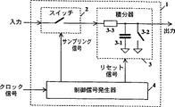
図1Aは、本発明に係る電荷サンプリング(CS)回路1の第1の実施の形態を示す。これは、サンプリング・スイッチ2と、積分器3と、制御信号発生器4を備える。スイッチ2は、信号入力と、信号出力と、制御入力とを有する。アナログ信号がスイッチの信号入力に入る。これは電荷サンプリング回路1の信号入力であり、サンプリング信号は制御信号発生器4から制御入力に与えられる。サンプリング信号がサンプリング段階にあるときだけスイッチが導通する(すなわち、スイッチの信号入力が信号出力に接続する)。積分器3は、信号入力と、信号出力と、制御入力とを有する。スイッチ2の信号出力は積分器3の信号入力に与えられ、制御信号発生器4からのリセット信号は積分器3の制御入力に与えられる。サンプリング段階でCS回路1へのアナログ入力信号の電流を積分し、サンプリング段階の終わりに、積分電荷は比例電圧または電流サンプルをCS回路の信号出力に生成する。リセット信号が始まるリセット段階までこのサンプルは保持され、その間の時間間隔が保持段階である。これらの段階を繰り返すとサンプルのシーケンスが生成され、この信号出力は前記CS回路の信号出力である。前に述べたように、制御信号発生器4は、CS回路のクロック入力であるクロック入力と、スイッチ2の制御入力に接続するサンプリング信号出力と、積分器3の制御入力に接続するリセット信号出力とを有する。
FIG. 1A shows a first embodiment of a charge sampling (CS)
この実施の形態では、積分器3は、コンデンサ3−1と、リセット・スイッチ3−2と、オプションの抵抗器3−3を備える。しかし他の実施の形態では、積分器3は異なる構成を有してよい。アナログ信号はサンプリング・スイッチ2の入力に与えられる。上に述べたように、電荷サンプリング・プロセスはリセットとサンプリング(t1からt2)と保持の3連続段階を含む。時間t1からt2はサンプリング窓と定義される。図1Bはその動作波形を示す。リセット段階でリセット・スイッチ3−2だけが導通してコンデンサ3−1をリセットする。サンプリング段階でサンプリング・スイッチ2だけが導通して信号電流をコンデンサ3−1に積分する。時定数は、信号が電圧源から来るとき(これが普通)に直線充電を行うのに十分の大きさを有する。スイッチ2の導通抵抗が非常に小さい場合はオプションの抵抗3−3を追加してよい。保持段階で両スイッチは切断状態であり、更に用いるために積分器3の出力電圧を保持する。1対の相互接続されたCS回路で差動CS回路を形成すると、差動入力信号を用いてまた制御信号発生器4を共用することにより差動出力を与えて、コモン・モードの影響を打ち消す。CS回路または回路対を並列に用いると、サンプリング信号とリセット信号を時間的に交互配置することによりサンプリング速度を高め、また2つのサンプリング点の間の時間間隔をサンプリング窓より小さくすることができる。信号電流はI(t)=ΣIisin(ωit+φi)、i=1,2,...,m、で表すことができる。全積分電荷はQ=ΣQi、ただし、Qi=(Ii/ωi)(cos(ωit1+φi)−cos(ωit2+φi))である。tsがサンプリング窓の中心時刻で、2Δt=(t2-t1)が窓の幅の場合はQ1=(2sin(ωiΔt/ωi)Iisin(ωits+φi)=2Δt(sin(ωiΔt)/(ωiΔt))Iisin(ωits+φi)である。
In this embodiment, the
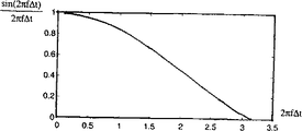
tsでの第i成分の瞬時値Ii(ts)=Iisin(ωits+φi)と比べると、差はki=2Δt(sin(ωiΔt/ωiΔt))であり、サンプリング係数は周波数ωiとΔtに依存する。この係数を用いると、時刻tsで第i周波数成分を正確にサンプリングすることができる。全ての周波数成分をtsでサンプリングするので、コンデンサ上の全電荷は当然tsでの信号サンプルを表す。すなわち、tsは等価サンプリング時点である。図1Cに示すように、CS回路の周波数応答は関数sin(ωiΔt/ωiΔt)に依存する。解像度に関係なく、その3dB帯域幅はΔf3dB=1.4/(2πΔt)(すなわち、450psのサンプリング窓で1GHz)である。しかし電圧サンプリングでは、1GHzで8ビットの解像度を得るためにはサンプリング隙間は1psより小さくなければならない。関数sin(ωiΔt/ωiΔt)は正確に定義されるので周波数の補償は可能である。1つの方法は、サンプリングの前に(ωiΔt)/sin(ωiΔt)の周波数応答を持つネットワークにアナログ信号を通すことである。別の方法は、A/D変換の後にディジタル信号処理プロセッサ(DSP)を用いて周波数応答を補償することである。 the i component of the instantaneous value I i at t s (t s) = I i sin (ω i t s + φ i) and compared, the difference k i = 2Δt (sin (ω i Δt / ω i Δt)) And the sampling coefficient depends on the frequencies ω i and Δt. Using this factor, it is possible to accurately sample the i frequency component at time t s. Since sampling all frequency components at t s, representing the signal samples in total charge naturally t s on the capacitor. That, t s is the equivalent sampling time point. As shown in FIG. 1C, the frequency response of the CS circuit depends on the function sin (ω i Δt / ω i Δt). Regardless of resolution, the 3 dB bandwidth is Δf 3dB = 1.4 / (2πΔt) (ie, 1 GHz with a 450 ps sampling window). However, in voltage sampling, the sampling gap must be smaller than 1 ps in order to obtain 8-bit resolution at 1 GHz. Since the function sin (ω i Δt / ω i Δt) is accurately defined, frequency compensation is possible. One method is to pass the analog signal through a network with a frequency response of (ω i Δt) / sin (ω i Δt) before sampling. Another method is to compensate the frequency response using a digital signal processor (DSP) after A / D conversion.
また、帯域通過電荷サンプリング(BPCS)回路は2個のスイッチと、重みおよびサンプリング(W&S)要素と、積分器と、制御信号発生器とを備える。制御信号発生器は、クロックと、反転クロックと、W&S信号と、リセット信号とを生成する。差動信号の2端を2つのスイッチ入力にそれぞれ与える。クロックと反転クロックによりそれぞれ制御される2個のスイッチは交互に導通する。両スイッチの出力をW&S要素の入力に与え、W&S要素の出力を積分器の入力に与える。これはリセットとサンプリングと保持の3連続段階で動作する。リセット段階ではリセット信号で積分器をリセットする。各サンプリング段階はnクロック・サイクルを含み、その間に信号電流をW&S要素で重みを付けて積分器で積分する。保持段階で積分器の出力を保持する。 The bandpass charge sampling (BPCS) circuit also includes two switches, weight and sampling (W & S) elements, an integrator, and a control signal generator. The control signal generator generates a clock, an inverted clock, a W & S signal, and a reset signal. Two ends of the differential signal are applied to two switch inputs, respectively. The two switches controlled by the clock and the inverted clock are turned on alternately. The outputs of both switches are applied to the input of the W & S element, and the output of the W & S element is applied to the input of the integrator. This operates in three successive stages of reset, sampling and holding. In the reset stage, the integrator is reset with a reset signal. Each sampling stage includes n clock cycles during which the signal current is weighted with a W & S element and integrated with an integrator. Hold the integrator output in the hold phase.
帯域通過電荷サンプリング(BPCS)回路5を図2Aに示す。これは2個のスイッチ2Aおよび2Bと、重みおよびサンプリング(W&S)要素6と、積分器3と、制御信号発生器7とを備える。制御信号発生器7は、クロックと、反転クロックと、W&S信号と、リセット信号とを生成する。差動アナログ信号の2端をスイッチ2Aおよび2Bの入力にそれぞれ与える。スイッチ2Aおよび2Bはクロックと反転クロックによりそれぞれ制御されて交互に導通する。スイッチ2Aおよび2Bの出力を共にW&S要素6の入力に与える。W&S要素6を通る電流はW&S信号で制御する。W&S要素6の出力を積分器3の入力に与える。各BPCSプロセス毎に、リセットとサンプリングと保持の3連続段階を行う。図2Bは動作波形を示す。リセット段階で積分器をリセットする。各サンプリング段階はnクロック・サイクルを含み、サンプリング窓を形成する。W&S要素を通る信号電流は、サンプリング窓の外ではゼロであり、サンプリング窓の中では重み関数(一定、直線、ガウス、またはその他の関数)に従ってこれに重みを付ける。重み関数はW&S要素6とW&S信号の組み合わせに依存する。図2Bに示す3つのW&S信号は3つの重み関数(一定、直線、ガウス)に対応し、特にW&S要素で用いて電流をW&S信号で線形制御する。保持段階で、更に用いるために積分器3の出力電圧を保持する。
A bandpass charge sampling (BPCS)
差動BPCS回路8を図3に示す。これは図のように接続される4個のスイッチ2A,2B,2C,2Dと、差動W&S(D−W&S)要素9と、差動積分器10と、制御信号発生器7とを備える。図に示す型のD−W&S要素9は2個の並列W&S要素6Aおよび6Bを備え、また図に示す型の差動積分器は2個の並列積分器3Aおよび3Bを備える。D−W&S要素9と差動積分器10は他の型でもよい。差動BPCS回路8は単一端のBPCS回路5と同様に動作するが、異なる点は2つの出力を差動的に生成することである。差動BPCS回路8はコモン・モードの影響を効果的に打ち消し、より正確な結果を得ることができる。
A
図4は並列差動BPCS回路11を示す。これは図のように接続される4個のスイッチ2A,2B,2C,2Dと,多数のD−W&S要素9A,9B,...,9Xと、多数の差動積分器10A,10B,...,10Xと、マルチプレクサ(MUX)12と、制御信号発生器13とを備える。D−W&S要素と差動積分器の各対9A+10A,9B+10B,...,9X+10Xはスイッチ2A,2B,2C,2Dと共に差動BPCS回路8と同様に動作する。これらの対へのW&S信号とリセット信号は制御信号発生器13で生成して均一に時間的に交互配置する。MUX12は制御信号発生器13からの多重化信号により制御され、保持段階で差動積分器10A,10B,...,10Xの出力を多重化して差動出力に与える。全体として、並列BPCS回路は一層高いサンプリング速度を与え、2連続サンプリング点の間の時間間隔をサンプリング窓よりも小さくすることができる。スイッチ2Cおよび2Dを除き、また差動W&S要素と差動積分器を単一端のものに置き換えると、並列単一端BPCS回路になる。
FIG. 4 shows the parallel
BPCS回路の濾波機能を図5に示す。上から順に、周波数はDCから3fcまで増加する。ただし、fcはクロック周波数である。負のクロック位相では同じ信号が逆に接続されることに注意していただきたい。図では信号の符号を変えてこれを表している。nクロック・サイクルの間積分して生成された電荷の正規化された振幅(すなわち、面積の和)を図5にそれぞれ示す。明らかであるが、fcより非常に高いまたは低い周波数を持つ入力信号では、電荷はほとんど完全に互いに打ち消されるので出力はほぼゼロである。fc/4,fc/2,2fc,...,などの周波数の入力信号では、その位相に関わらず電荷は完全に打ち消される。fcに近い周波数の入力信号では、電荷は部分的に打ち消される。fin=fcのときは、fcと同相の場合は電荷は完全に加算され、fcからπ/2の位相の場合(図5に示さず)は電荷は完全に打ち消される。信号の電荷を効果的に積分することができる帯域幅がある。この帯域幅の外では信号の電荷は完全にすなわち実質的に打ち消される。これは明らかに濾波機能である。これは、帯域幅の外の周波数の雑音も打ち消されることを意味する。 The filtering function of the BPCS circuit is shown in FIG. In order from the top, the frequency is increased from DC to 3f c. Where f c is the clock frequency. Note that the same signal is connected in reverse at negative clock phase. In the figure, this is shown by changing the sign of the signal. The normalized amplitude (ie, area sum) of the charge generated by integration over n clock cycles is shown in FIG. As will be apparent, the input signal having a very high or low frequencies than f c, the output is almost zero since the charge is almost completely canceled out each other. f c / 4, f c / 2,2f c,. . . In the case of an input signal having a frequency such as,, the charge is completely canceled regardless of the phase. The input signal of a frequency close to f c, the charge is partially canceled. When the f in = f c, the charge in the case of f c and phase are completely added, if the f c of [pi / 2 phase (not shown in FIG. 5) the charge is completely canceled. There is a bandwidth that can effectively integrate the charge of the signal. Outside this bandwidth, the signal charge is completely or substantially canceled. This is clearly a filtering function. This means that noise at frequencies outside the bandwidth is also canceled.
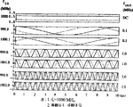
BPCSの理想的な周波数応答を図6Aに示す。これはサンプリング窓の中の信号電流の数学的に正確な積分に対応する。図6Aでは、n=10のとき一定重みと仮定する。これは、10クロック・サイクルのサンプリング窓の中で電流の重みを一定に保つことを意味する。また図6Aはfin=0からfin=8fcまでの周波数応答を示す。ここで、y軸は全周波数範囲内の最大出力振幅で正規化された種々の周波数の最大出力振幅であり、x軸はfcで正規化された入力周波数である。図から分かるように、fin>2fcの後は同じ周波数応答が繰り返されるが振幅は小さくなる。2(p−1)fc≦fin≦2pfcでは、出力周波数foutは|fin−(2p−1)fc|に等しい。ただしpは整数(≧1)である。fin=(2p−1)fcのとき出力はDC電圧であり、その振幅はfinとfcの位相関係に依存する。所定のpでは、(2p−1)fc−fin1=fin2−(2p−1)fcのとき、入力周波数fin1(<(2p−1)fc)とfin2(>(2p−1)fc)について同じ出力周波数が生成されるが、位相は異なる。図6Bは、fc=1000MHzのとき種々の入力周波数での出力サンプル波形をI相(実線)とQ相(点線)について示す。これは、BPCS回路が同時にフィルタとミクサとサンプラであることを示す。 The ideal frequency response of BPCS is shown in FIG. 6A. This corresponds to a mathematically exact integration of the signal current in the sampling window. In FIG. 6A, a constant weight is assumed when n = 10. This means that the current weight is kept constant within a 10 clock cycle sampling window. The Figure 6A shows the frequency response from f in = 0 to f in = 8f c. Here, y-axis is the maximum output amplitude of different frequency normalized by the maximum output amplitude in the whole frequency range, x-axis is the input frequency normalized by f c. As can be seen, although the same frequency response is repeated amplitude after f in> 2f c is reduced. For 2 (p−1) f c ≦ f in ≦ 2pf c , the output frequency f out is equal to | f in − (2p−1) f c |. However, p is an integer (≧ 1). When f in = (2p−1) f c , the output is a DC voltage, and its amplitude depends on the phase relationship between f in and f c . For a given p, when (2p-1) f c -f in1 = f in2- (2p-1) f c , the input frequencies f in1 (<(2p-1) f c ) and f in2 (> (2p -1) The same output frequency is generated for fc ) but the phase is different. FIG. 6B shows output sample waveforms at various input frequencies when f c = 1000 MHz for the I phase (solid line) and the Q phase (dotted line). This indicates that the BPCS circuit is simultaneously a filter, a mixer and a sampler.
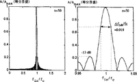
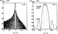
図7Aと図7Bは、n=50とn=500のときの一定重みBPCS回路の理想的な周波数応答をそれぞれ示す。図7Aはn=50のとき、範囲0<fin<2fcと、小さな範囲0.95fc<fin<1.05fcの周波数応答を示す。図7Bはn=500のとき、範囲0<fin<2fcと、小さな範囲0.995fc<fin<1.005fcの周波数応答を示す。図から分かるように、N=50のときΔf3dB=0.018fcであり、N=500のときΔf3dB=0.0018fcである。すなわち、帯域幅はnに逆比例する。遠端の周波数成分の振幅はnの増加と共に減少するが、最大隣接ピークはどちらの場合もほとんど変わらず、−13dB付近である。
7A and 7B show the ideal frequency response of a constant weight BPCS circuit when n = 50 and n = 500, respectively. FIG. 7A shows the frequency response of the
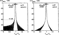
n=50とn=500のときの直線重みBPCS回路の理想的な周波数応答を図8Aと図8Bにそれぞれ示す。直線重みは、サンプリング段階で電流の重みが最初は直線的に増加し、次に、サンプリング窓の中心に対称に直線的に減少することを意味する。図8Aは、n=50のとき、範囲0<fin<2fcと、小さな範囲0.9fc<fin<1.1fcの周波数応答を示す。図8Bはn=500のとき、範囲0<fin<2fcと、小さな範囲0.99fc<fin<1.01fcの周波数応答を示す。図から分かるように、n=50のときΔf3dB=0.025fcであり、n=500のときΔf3dB=0.0025fcであって、一定重みの場合に比べてやや増加している。遠端の周波数成分の振幅はnの増加と共に急速に減少する。一定重みの場合に比べて、最大隣接ピークは−26dBと−27dBにそれぞれ減少する。
The ideal frequency response of the linear weight BPCS circuit when n = 50 and n = 500 is shown in FIGS. 8A and 8B, respectively. The linear weight means that at the sampling stage, the current weight first increases linearly and then decreases linearly symmetrically about the center of the sampling window. Figure 8A, when the n = 50, indicating the
図9Aと図9Bは、ガウス重みBPCS回路の理想的な周波数応答を示す。ガウス重みは、サンプリング段階で電流の重みが、サンプリング窓の中心に対称に所定のσでガウス関数exp(−t2/2σ2)に従って変化することを意味する。比Δt/σは重みパラメータである。ただし、Δtはサンプリング窓の半分、σは標準偏差である。図9Aは、範囲0<fin<2fcで、n=75のときΔt/σ=3.5と、n=87のときΔt/σ=4におけるそれぞれの周波数応答を示す。3dB帯域幅は共に0.025fcである。図9Bは、範囲0.9fc<fin<1.1fcで、n=750のときΔt/σ=3.5と、n=870のときΔt/σ=4におけるそれぞれの周波数応答を示す。3dB帯域幅は共に0.0025fcである。遠端の周波数成分と隣接ピークの振幅はガウス重みと共に実質的に減少する。最大隣接ピークは−61dBから−78dBの範囲である。
9A and 9B show the ideal frequency response of a Gaussian weight BPCS circuit. The Gaussian weight means that the current weight changes according to the Gaussian function exp (−t 2 / 2σ 2 ) with a predetermined σ symmetrically about the center of the sampling window in the sampling stage. The ratio Δt / σ is a weight parameter. Where Δt is half the sampling window and σ is the standard deviation. 9A is in the
n−MOSトランジスタを用いた差動BPCS回路8のコアの実施の形態14を図10に示す。クロックされるスイッチはn−MOSトランジスタ15A,15B,15C,15Dである。W&S要素はn−MOSトランジスタ16Aと16Bである。リセット・スイッチはn−MOSトランジスタ18Aと18Bである。コンデンサはオンチップMOSコンデンサ17Aと17Bである。クロックは正弦波であるが、準方形波を用いてもよい。実施の形態14は全てのCMOSプロセスで動作する。しかし0.8μmCMOSプロセスのパラメータはHSPICEシミュレーションで用いられる。次の3つの実施の形態は、特定の成分値とW&S信号パラメータを持つ実施の形態14に基づいている。
FIG. 10 shows a fourteenth embodiment of the core of the
n=10のとき、fc=1000MHzにおける一定重みの実施の形態19を図11Aに示す。クロックされるスイッチはn−MOSトランジスタ20A,20B,20C,20Dである。W&S要素はn−MOSトランジスタ21Aと21Bである。リセット・スイッチはn−MOSトランジスタ23Aと23Bである。これらは全て最小のサイズ、2μm/0.8μm(幅/長さ)を有する。コンデンサはMOSコンデンサ22Aと22Bで、共に40pFである。一定重みW&S信号の幅は、n=10に対応する10nsである。最大差動出力サンプル電圧は約100mVである。図11Bは、fin=900−1100MHzにおける理論的周波数応答を実線で、HSPICEシミュレーションによる周波数応答を点線で示す。シミュレーションによる周波数応答は理論的周波数応答にほぼ従う。両方とも、最大隣接ピークは−13dBで、Δf3dB=18MHzである。
FIG. 11A shows a nineteenth embodiment with a constant weight at f c = 1000 MHz when n = 10. The clocked switches are n-
n=59のとき、fc=1000MHzにおける直線重みの実施の形態24を図12Aに示す。クロックされるスイッチはn−MOSトランジスタ25A,25B,25C,25Dで、全て大きなサイズの10μm/0.8μmを有する。これにより、信号電流はスイッチではなくW&S要素により左右される。W&S要素はn−MOSトランジスタ21Aと21Bで、2μm/0.8μmである。リセット・スイッチはn−MOSトランジスタ23Aと23Bで、2μm/0.8μmである。コンデンサはMOSコンデンサ22Aと22Bで、共に40pFである。直線重みW&S信号の幅は、n=59に対応する59nsである。最大差動出力サンプル電圧は約100mVである。図12Bは、fin=900−1100MHzにおける理論的周波数応答を実線で、HSPICEシミュレーションによる周波数応答を点線で示す。シミュレーションによる周波数応答は基本的に理論的周波数応答に従う。両方とも、Δf3dB=21MHzである。しかし実施の形態24では、最大隣接ピークは−30dBで、理論的応答のピークより小さい。これは、n−MOSトランジスタ21Aまたは21Bのコンダクタンスが直線W&S信号と共に直線的に変わらないからである。実際の重み関数は直線とガウスの中間である。
FIG. 12A shows a twenty-fourth embodiment of linear weighting at f c = 1000 MHz when n = 59. The clocked switches are n-
n=599のとき、fc=1000MHzにおける直線重みの実施の形態26を図13Aに示す。クロックされるスイッチはn−MOSトランジスタ25A,25B,25C,25Dで、10μm/0.8μmである。W&S要素はn−MOSトランジスタ27Aと27Bで、2μm/16μmである。注意すべきであるが、27Aと27Bの長さを16μmの大きさにして、かかる長い充電時間(599ns)中、信号電流とコンデンサ電圧を制限する。リセット・スイッチはn−MOSトランジスタ23Aと23Bで、2μm/0.8μmである。コンデンサはMOSコンデンサ28Aと28Bで、共に20pFである。直線重みW&S信号の幅は、n=599に対応する599nsである。最大差動出力サンプル電圧は約100mVである。図13Bは、fin=990−1010MHzにおける理論的周波数応答を実線で、HSPICEシミュレーションによる周波数応答を点線で示す。シミュレーションによる周波数応答は基本的に理論的周波数応答に従う。両方とも、Δf3dB=2MHzである。上に述べたのと同じ理由から、実施の形態26の最大隣接ピークは−30dBであり、理論的応答のピークより小さい。
FIG. 13A shows a twenty-sixth embodiment of linear weighting at f c = 1000 MHz when n = 599. The clocked switches are n-
図14Aと図14Bは、出力の揺れと直線性を改善する能動積分器それぞれを示す。単一端の能動積分器29を図14Aに示す。これは、図のように接続された差動入力単一出力増幅器30と、インバータ35と、コンデンサ31と、スイッチ32,33,34とを備える。能動積分器は信号入力を常に実質的に接地に保って、コンデンサ電圧が信号電流に与える影響を除去する。増幅器30の帯域幅は信号のベースバンドをカバーするだけでよく、搬送波をカバーする必要はない。これは実現可能である。インバータ35はリセット信号を入力として用いて遅れを持つ反転リセット信号を生成してスイッチ33を制御し、リセット信号はスイッチ32と34を制御する。リセット段階でスイッチ32と34は導通してスイッチ33は切れる。コンデンサ31の電圧はリセットされて増幅器30の入力オフセット電圧になる。サンプリング段階でスイッチ32と34は切れてスイッチ33は導通する。コンデンサ31は信号電流により充電される。同時に、増幅器30のオフセット電圧は打ち消される。差動能動積分器36を図14Bに示す。これは差動入力差動出力増幅器37と、2個のコンデンサ31Aと31Bと、インバータ35と、スイッチ32A,32B,33A,33B,34A,34Bとを備える。これは基本的に積分器29と同様に動作するが、異なる点は差動入力信号を用いて差動出力を生成することである。積分器29は図1Aの積分器3の代わりに用いよく、積分器36は図3の積分器10の代わりに用いてよい。
14A and 14B show active integrators that improve output swing and linearity, respectively. A single-ended
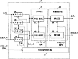
図15は2ステップBPCS回路38を示す。これは第1のBPCS回路39と、チョッピング回路40と、増幅器41と、第2のBPCS回路42と、第2のクロックを生成するクロック信号発生器43とを備える。第1のBPCS回路39と第2のBPCS回路42はBPCS回路5,8,11,19,24,26のどの型でもよい。第1のBPCS回路39の2入力に差動アナログ信号の2端をそれぞれ与え、そのクロック入力に第1のクロックを与える。第1のサンプリング速度を持つ信号サンプルを第1のBPCS回路39で生成してチョッピング回路40に与え、第2のクロックで制御してサンプルを時間的に対称にチョッピングする。チョッピング周波数と同じ新しい搬送波周波数を持つチョッピングされた信号をチョッピング回路40から増幅器41に与え、増幅された差動信号を第2のBPCS回路42の2入力にそれぞれ与える。第2のクロックの制御により、第2のBPCS回路42は第2のサンプリング速度を持つ最終サンプル出力を生成する。2ステップBPCS回路38は性能のトレードオフに柔軟性を与える。2ステップBPCS回路38に基づいて、更に多くのステップのBPCS回路を構築することができる。
FIG. 15 shows a two-
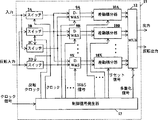
フロントエンド・サンプリング無線受信機構造44を図16に示す。これは、fpass<2fcを持つ低域フィルタ45と、差動出力低雑音増幅器(LNA)46と、2つのBPCS回路47Aと47Bと、90°移相器48と、ローカル発振器49とを備える。アンテナからの無線信号は低域フィルタ45の入力に入る。2fcを超える周波数成分は大幅に減衰する。低域フィルタ45の出力をLNA46に与え、十分大きな振幅を持つ差動出力を生成する。差動出力をBPCS回路47Aと47Bの入力に同時に与える。同時に、ローカル発振器49が生成するIクロック信号をBPCS回路47Aに与え、90°移相器がIクロック信号から生成するQクロック信号をBPCS回路47Bに与える。BPCS回路47Aと47BはIサンプルとQサンプルをそれぞれ生成する。サンプル出力は、直ぐディジタル・データに変換してもよいし、更に処理してもよい。BPCS回路47Aと47BはBPCS回路5,8,11,19,24,26のどれでもよい。これらの回路内の積分器は受動積分器でもよいし能動積分器でもよい。無線受信機構造44はフロントエンドに濾波機能と混合機能とサンプリング機能を同時に有するので、A/D変換の性能要求が緩和され、アナログ・フィルタが不要になり、DSPの機能が高度に利用される。原理的に、任意の狭い帯域幅(すなわち、任意の高いQ値)が可能である。濾波機能の中心周波数は容易にプログラムすることができる。これは広い応用範囲を持つ優れた無線通信機構造である。
A front end sampling
CSおよびBPCS回路に用いられるサンプリング・コンデンサは電圧サンプリング回路に用いられるものよりはるかに大きいので、雑音が少なく、充電とクロックのフィードスルーが低い。 Sampling capacitors used in CS and BPCS circuits are much larger than those used in voltage sampling circuits, so there is less noise and charge and clock feedthrough is low.
BPCS回路は同時に、無線周波数で動作するフィルタとミクサとサンプラである。中心周波数と帯域幅と隣接選択性は、クロック周波数と数nとW&S信号波形により設定することできる。これはフロントエンド・サンプリング無線受信機とシステム・オン・チップに特に有用である。 The BPCS circuit is simultaneously a filter, mixer and sampler operating at radio frequencies. The center frequency, bandwidth, and adjacent selectivity can be set by the clock frequency, the number n, and the W & S signal waveform. This is particularly useful for front-end sampling radio receivers and system-on-chip.
理解されるように、この明細書では本発明の多くの特徴と機能を、本発明の機能の詳細と共に示したが、この開示は単なる例であって、特許請求の範囲に規定されている本発明の範囲内で詳細を変更することできる。 As will be appreciated, while the specification has presented a number of features and functions of the invention, along with details of the functions of the invention, this disclosure is only an example and the present invention as defined in the claims Details may be changed within the scope of the invention.
Claims (15)
前記第1のBPCS回路(39)内の差動アナログ信号の第1の端と第2の端をそれぞれ受けて、前記第1のBPCS回路の信号出力または出力対で信号サンプルを第1のサンプリング速度で生成する第1の信号入力と第2の信号入力と、
前記第1のBPCS回路(39)からの信号を時間的に対称に前記第1のサンプリング速度に等しいクロック信号の周波数でその信号出力または出力対でチョッピングするチョッピング回路(40)と、
前記チョッピング回路からの信号を差動的にその信号出力対で増幅する差動出力増幅器(41)と、
を備え、
前記第2のBPCSの第1の信号入力と第2の信号入力は前記増幅器(41)の信号出力対に接続して、信号サンプルを第2のサンプリング速度で信号出力または出力対で生成することを特徴とする2ステップBPCS回路。 A two-step BPCS circuit comprising the first and second BPCS circuits (39, 42) according to any one of the preceding claims,
Receiving the first end and the second end of the differential analog signal in the first BPCS circuit (39), respectively, the first BPCS circuit outputs a signal sample or a signal sample at a first sampling by a signal output or an output pair. A first signal input and a second signal input generated at a speed;
A chopping circuit (40) for chopping the signal from the first BPCS circuit (39) with its signal output or output pair at a frequency of a clock signal equal to the first sampling rate symmetrically in time;
A differential output amplifier (41) for differentially amplifying a signal from the chopping circuit with the signal output pair;
With
The first signal input and the second signal input of the second BPCS are connected to the signal output pair of the amplifier (41) to generate signal samples at the signal output or output pair at a second sampling rate. A two-step BPCS circuit characterized by
ドレンを信号入力とし、ゲートを制御入力とし、ソースを信号出力とする、n−MOSトランジスタを備える前記スイッチのn−MOS構成と、
ドレンを互いに接続して信号入力とし、ソースを互いに接続して信号出力とし、前記n−MOSトランジスタのゲートを制御入力とする、n−MOSトランジスタおよびp−MOSトランジスタと、入力を前記n−MOSトランジスタのゲートに接続し、出力を前記p−MOSトランジスタのゲートに接続するインバータと、を備える前記スイッチのCMOS構成と、
ドレンを信号入力とし、ゲートを制御入力とし、ソースを信号出力とするn−MOSトランジスタを備える前記W&S要素の構成と、
第1の端を信号入力とし、第2の端を接地するコンデンサと、必要に応じて前記信号入力と前記コンデンサの第1の端の間に挿入するオプションの抵抗器と、ドレンとソースを前記コンデンサの第1の端と第2の端にそれぞれ接続し、ゲートを制御入力とするn−MOSトランジスタと、を備える前記積分器の受動構成と、
信号入力と信号出力をそれぞれ前記差動積分器の第1の信号入力と第1の信号出力とする前記積分器の第1の受動構成と、信号入力と信号出力をそれぞれ前記差動積分器の第2の信号入力と第2の信号出力とする前記積分器の第2の受動構成と、を備える前記差動積分器の受動構成と、
正入力を接地し、負入力を前記積分器の信号入力とし、出力を前記積分器の信号出力とする差動入力単一出力増幅器と、第1の端を前記差動入力単一出力増幅器の負入力に接続するコンデンサと、入力を前記積分器の制御入力とするインバータと、信号入力を前記差動入力単一出力増幅器の負入力に接続し、制御入力を前記積分器の制御入力に接続し、信号出力を前記差動入力単一出力増幅器の出力に接続する前記スイッチの第1のn−MOSまたはCMOS構成と、信号入力を前記コンデンサの第2の端に接続し、制御入力を前記積分器の制御入力に接続し、信号出力を接地する前記スイッチの第2のn−MOSまたはCMOS構成と、信号入力を前記コンデンサの第2の端に接続し、制御入力を前記インバータの出力に接続し、信号出力を前記差動入力単一出力増幅器の出力に接続する前記スイッチの第3のn−MOSまたはCMOS構成と、必要に応じて前記積分器の信号入力と前記差動入力単一出力増幅器の負入力の間に挿入するオプションの抵抗器と、を備える前記積分器の能動構成と、
負入力と、正入力と、正出力と、負出力を前記差動積分器の第1の信号入力と、第2の信号入力と、第1の信号出力と、第2の信号出力とする差動入力差動出力増幅器と、第1の端を前記差動入力差動出力増幅器の負入力に接続する第1のコンデンサと、第1の端を前記差動入力差動出力増幅器の正入力に接続する第2のコンデンサと、入力を前記差動積分器の制御入力とするインバータと、信号入力を前記差動入力差動出力増幅器の負入力に接続し、制御入力を前記差動積分器の制御入力に接続し、信号出力を前記差動入力差動出力増幅器の正出力に接続する、前記スイッチの第1のn−MOS構成またはCMOS構成と、信号入力を前記第1のコンデンサの第2の端に接続し、制御入力を前記差動積分器の制御入力に接続し、信号出力を接地する前記スイッチの第2のn−MOS構成またはCMOS構成と、信号入力を前記第1のコンデンサの第2の端に接続し、制御入力を前記インバータの出力に接続し、信号出力を前記差動入力差動出力増幅器の正出力に接続する前記スイッチの第3のn−MOS構成またはCMOS構成と、信号入力を前記差動入力差動出力増幅器の正入力に接続し、制御入力を前記差動積分器の制御入力に接続し、信号出力を前記差動入力差動出力増幅器の負入力に接続する前記スイッチの第4のn−MOS構成またはCMOS構成と、信号入力を前記第2のコンデンサの第2の端に接続し、制御入力を前記差動積分器の制御入力に接続し、信号出力を接地する前記スイッチの第5のn−MOS構成またはCMOS構成と、信号入力を前記第2のコンデンサの第2の端に接続し、制御入力を前記インバータの出力に接続し、信号出力を前記差動入力差動出力増幅器の負出力に接続する前記スイッチの第6のn−MOS構成またはCMOS構成と、必要に応じて前記差動積分器の第1の信号入力と前記差動入力差動出力増幅器の負入力の間に挿入する第1のオプションの抵抗器と、必要に応じて前記差動積分器の第2の信号入力と前記差動入力差動出力増幅器の正入力の間に挿入する第2のオプションの抵抗器と、を備える前記差動積分器の能動構成と、
を備えることを特徴とするビルディング・ブロックの構成。 A configuration of the building blocks in any kind of BPCS circuit according to any one of claims 1 to 11,
An n-MOS configuration of the switch comprising an n-MOS transistor having a drain as a signal input, a gate as a control input, and a source as a signal output;
An n-MOS transistor and a p-MOS transistor having drains connected to each other as a signal input, sources connected to each other as a signal output, a gate of the n-MOS transistor as a control input, and an input as the n-MOS A CMOS configuration of the switch comprising: an inverter connected to a gate of a transistor and an output connected to a gate of the p-MOS transistor;
A configuration of the W & S element including an n-MOS transistor having a drain as a signal input, a gate as a control input, and a source as a signal output;
A capacitor having a first end as a signal input and a second end grounded, an optional resistor inserted between the signal input and the first end of the capacitor, if necessary, a drain and a source A passive configuration of the integrator comprising: an n-MOS transistor connected to a first end and a second end of the capacitor, respectively, and having a gate as a control input;
A first passive configuration of the integrator having a signal input and a signal output respectively as a first signal input and a first signal output of the differential integrator; and a signal input and a signal output of the differential integrator, respectively. A passive configuration of the differential integrator comprising: a second passive configuration of the integrator for providing a second signal input and a second signal output;
A differential input single output amplifier having a positive input grounded, a negative input as a signal input of the integrator, and an output as a signal output of the integrator; and a first end of the differential input single output amplifier. A capacitor connected to the negative input, an inverter whose input is the control input of the integrator, a signal input is connected to the negative input of the differential input single output amplifier, and a control input is connected to the control input of the integrator A first n-MOS or CMOS configuration of the switch for connecting a signal output to the output of the differential input single output amplifier; a signal input connected to a second end of the capacitor; A second n-MOS or CMOS configuration of the switch that connects to the control input of the integrator and grounds the signal output; a signal input to the second end of the capacitor; and a control input to the output of the inverter Connect and signal output A third n-MOS or CMOS configuration of the switch connected to the output of the differential input single output amplifier, and optionally the signal input of the integrator and the negative input of the differential input single output amplifier. An active configuration of the integrator comprising an optional resistor interposed therebetween;
Difference between negative input, positive input, positive output, and negative output as first signal input, second signal input, first signal output, and second signal output of the differential integrator A dynamic input differential output amplifier, a first capacitor connecting a first end to the negative input of the differential input differential output amplifier, and a first end to the positive input of the differential input differential output amplifier. A second capacitor to be connected; an inverter having an input as a control input of the differential integrator; a signal input connected to a negative input of the differential input differential output amplifier; and a control input of the differential integrator A first n-MOS or CMOS configuration of the switch, connected to a control input, and connecting a signal output to a positive output of the differential input differential output amplifier, and a signal input to a second of the first capacitor. Connect the control input to the control input of the differential integrator and connect the signal output to A second n-MOS configuration or a CMOS configuration of the switch, a signal input connected to a second end of the first capacitor, a control input connected to an output of the inverter, and a signal output connected to the difference A third n-MOS or CMOS configuration of the switch connected to the positive output of the dynamic input differential output amplifier; a signal input connected to the positive input of the differential input differential output amplifier; and a control input connected to the differential input A fourth n-MOS or CMOS configuration of the switch, connected to the control input of the dynamic integrator and connecting the signal output to the negative input of the differential input differential output amplifier, and the signal input to the second capacitor A fifth n-MOS configuration or a CMOS configuration of the switch for connecting a control input to a control input of the differential integrator and grounding a signal output; and a signal input of the second integrator Conde of A sixth n-MOS configuration or CMOS of the switch that connects to the second end of the switch, connects the control input to the output of the inverter, and connects the signal output to the negative output of the differential input differential output amplifier A first optional resistor inserted between the first signal input of the differential integrator and the negative input of the differential input differential output amplifier, if necessary, and the difference if necessary An active configuration of the differential integrator comprising: a second optional resistor inserted between a second signal input of the dynamic integrator and a positive input of the differential input differential output amplifier;
A building block structure characterized by comprising:
前記クロック周波数の2倍以下の帯域幅を持ち、無線信号を受信して濾波する低域フィルタ(45)と、
差動的に増幅された無線信号を前記濾波された信号から生成する低雑音増幅器(46)と、
Iクロック信号をその信号出力に生成するローカル発振器(49)と、
信号入力を前記ローカル発振器(49)に接続して、前記Iクロック信号と同じ振幅でπ/2位相シフトしたQクロック信号をその信号出力に生成するπ/2移相器(48)と、
を備え、
前記低雑音増幅器(46)の信号出力対の2端を前記第1のBPCS回路(47A)と第2のBPCS回路(47B)にそれぞれ接続し、前記Iクロック信号出力を前記第1のBPCS回路(47A)のクロック入力に接続し、前記Qクロック信号出力を前記第2のBPCS回路(47B)のクロック入力に接続して、前記無線信号のベースバンドIサンプルを前記第1のBPCS回路(47A)の信号出力または出力対で生成し、前記無線信号のベースバンドQサンプルを前記第2のBPCS回路(47B)の信号出力または出力対で生成することを特徴とするフロントエンド・サンプリング無線受信装置。 A front-end sampling radio reception apparatus comprising the first and second BPCS circuits according to any one of claims 1 to 11 ,
A low pass filter (45) having a bandwidth less than twice the clock frequency and receiving and filtering radio signals;
A low noise amplifier (46) for generating a differentially amplified radio signal from the filtered signal;
A local oscillator (49) for generating an I clock signal at its signal output;
A π / 2 phase shifter (48) for connecting a signal input to the local oscillator (49) and generating a Q clock signal shifted in phase by π / 2 with the same amplitude as that of the I clock signal;
With
Two ends of the signal output pair of the low noise amplifier (46) are connected to the first BPCS circuit (47A) and the second BPCS circuit (47B), respectively, and the I clock signal output is connected to the first BPCS circuit. The Q clock signal output is connected to the clock input of the second BPCS circuit (47B), and the baseband I samples of the radio signal are connected to the first BPCS circuit (47A). ) And a baseband Q sample of the radio signal is generated by the signal output or output pair of the second BPCS circuit (47B). .
前記第1および第2のBPCS回路(47A,47B)の前記ローカル発振器(49)と前記移相器(48)と前記クロック発生器を組み合わせて、差動Iクロック信号およびQクロック信号を一層効果的にまた正確に生成し、
前記ベースバンドIサンプルおよびQサンプルを、2個の別個のアナログ・ディジタル変換器によりまたは単一の多重化アナログ・ディジタル変換器によりディジタル信号に変換し、
前記ディジタル信号をデジタル信号処理(DSP)ユニットで処理し、
前記フロントエンド・サンプリング無線受信装置は非常に簡単化されたアナログ部を有する優れたアナログ無線受信装置であり、またDSPの能力を高度に利用する、
ことを特徴とするフロントエンド・サンプリング無線受信装置。 The front-end sampling radio reception apparatus according to claim 13 ,
The local oscillator (49), the phase shifter (48), and the clock generator of the first and second BPCS circuits (47A, 47B) are combined with the clock generator to further enhance the differential I clock signal and Q clock signal. Accurately and accurately
Converting the baseband I and Q samples into digital signals by two separate analog-to-digital converters or by a single multiplexed analog-to-digital converter;
Processing the digital signal with a digital signal processing (DSP) unit;
The front-end sampling radio receiving apparatus is an excellent analog radio receiving apparatus having a very simplified analog unit, and highly utilizes the capability of the DSP.
A front-end sampling radio receiving apparatus.
前記W&S段階の終わりに比例電圧または電流サンプルを生成するステップと、
を含むことを特徴とする電荷サンプリングの方法。 Weighting the first and second ends of the differential analog signal in the W & S stage and integrating the weighted signal in the W & S stage, wherein the current of the weighted signal is integrated as an integral charge. Said step;
Generating a proportional voltage or current sample at the end of the W & S phase;
A method of charge sampling, comprising:
Applications Claiming Priority (2)
| Application Number | Priority Date | Filing Date | Title |
|---|---|---|---|
| SE9903532A SE9903532D0 (en) | 1999-09-28 | 1999-09-28 | Versatile charge sampling circuits |
| SE9903532-1 | 1999-09-28 |
Related Parent Applications (1)
| Application Number | Title | Priority Date | Filing Date |
|---|---|---|---|
| JP2001527292A Division JP4685310B2 (en) | 1999-09-28 | 2000-09-25 | Various charge sampling circuits |
Publications (2)
| Publication Number | Publication Date |
|---|---|
| JP2011103666A JP2011103666A (en) | 2011-05-26 |
| JP4875201B2 true JP4875201B2 (en) | 2012-02-15 |
Family
ID=20417207
Family Applications (2)
| Application Number | Title | Priority Date | Filing Date |
|---|---|---|---|
| JP2001527292A Expired - Fee Related JP4685310B2 (en) | 1999-09-28 | 2000-09-25 | Various charge sampling circuits |
| JP2010274877A Expired - Fee Related JP4875201B2 (en) | 1999-09-28 | 2010-12-09 | Various charge sampling circuits |
Family Applications Before (1)
| Application Number | Title | Priority Date | Filing Date |
|---|---|---|---|
| JP2001527292A Expired - Fee Related JP4685310B2 (en) | 1999-09-28 | 2000-09-25 | Various charge sampling circuits |
Country Status (9)
| Country | Link |
|---|---|
| US (3) | US7053673B1 (en) |
| EP (2) | EP2228800A3 (en) |
| JP (2) | JP4685310B2 (en) |
| CN (2) | CN1174431C (en) |
| AT (1) | ATE506677T1 (en) |
| AU (1) | AU7820100A (en) |
| DE (1) | DE60045867D1 (en) |
| SE (1) | SE9903532D0 (en) |
| WO (1) | WO2001024192A1 (en) |
Families Citing this family (18)
| Publication number | Priority date | Publication date | Assignee | Title |
|---|---|---|---|---|
| US7239183B2 (en) | 2003-09-29 | 2007-07-03 | Nokia Corporation | Active current mode sampling circuit |
| JP5046622B2 (en) | 2005-12-13 | 2012-10-10 | パナソニック株式会社 | Sampling filter device |
| US7671658B2 (en) | 2006-05-24 | 2010-03-02 | Panasonic Corporation | Mixer having frequency selection function |
| US8032094B2 (en) * | 2006-06-08 | 2011-10-04 | Panasonic Corporation | Discrete filter, sampling mixer, and radio device |
| JP2008017220A (en) * | 2006-07-06 | 2008-01-24 | Sony Corp | Charge domain filter circuit |
| WO2008050630A1 (en) | 2006-10-23 | 2008-05-02 | Panasonic Corporation | Sampling filter device and radio communication device |
| FR2911449B1 (en) * | 2007-01-16 | 2009-02-27 | Commissariat Energie Atomique | SAMPLE FILTER WITH FINITE IMPULSE RESPONSE |
| US8385874B2 (en) | 2007-03-06 | 2013-02-26 | Panasonic Corporation | Discrete time direct sampling circuit and receiver |
| US8274418B2 (en) | 2007-05-18 | 2012-09-25 | Nokia Corporation | Analogue-to-digital converter |
| US8711917B2 (en) | 2008-01-16 | 2014-04-29 | Panasonic Corporation | Sampling filter device |
| EP2483891A2 (en) * | 2009-09-28 | 2012-08-08 | Arctic Silicon Devices As | Input configuration for analog to digital converter |
| FR2954628B1 (en) | 2009-12-18 | 2012-02-24 | Commissariat Energie Atomique | DEVICE AND METHOD FOR RECEIVING RF SIGNALS BASED ON A HETERODYNE ARCHITECTURE WITH UNDER-SAMPLING COMPLEX IF |
| WO2012129271A1 (en) * | 2011-03-22 | 2012-09-27 | Ess Technology, Inc. | Finite impulse response filter for producing outputs having different phases |
| US9287851B2 (en) | 2011-03-22 | 2016-03-15 | Ess Technology, Inc. | Finite impulse response filter for producing outputs having different phases |
| ITFO20110009A1 (en) * | 2011-08-12 | 2013-02-13 | Marco Bennati | SYSTEM AND METHOD OF REDUCTION OF NOISE IN CHAMPIONSHIP AMPLIFIERS. |
| US20140049291A1 (en) | 2012-08-14 | 2014-02-20 | Luxen Technologies, Inc. | Noise-resistant sampling circuit and image sensor |
| CN107918443B (en) * | 2016-10-11 | 2020-04-24 | 深圳市中兴微电子技术有限公司 | Signal generation method and device |
| KR20230164443A (en) * | 2022-05-25 | 2023-12-04 | 삼성전자주식회사 | Clock Generator and Electronic Device including Clock Generator |
Family Cites Families (30)
| Publication number | Priority date | Publication date | Assignee | Title |
|---|---|---|---|---|
| IT1186340B (en) * | 1985-10-29 | 1987-11-26 | Sgs Microelettronica Spa | DIFFERENTIAL INTEGRATOR WITH SWITCHED CONDENSER USING A SINGLE INTEGRATION CONDENSER |
| JPS62145927A (en) * | 1985-12-20 | 1987-06-30 | Hitachi Ltd | data conversion device |
| IT1227615B (en) * | 1988-12-22 | 1991-04-22 | Sgs Thomson Microelectronics | FILTER COMPLETELY DIFFERENTIAL WITH SWITCHED CAPACITORS USING OPERATIONAL AMPLIFIERS CMOS WITHOUT COMMON MODE FEEDBACK |
| US5128966A (en) * | 1989-02-15 | 1992-07-07 | Samsung Electronics Co., Ltd. | System for demodulating frequency- or phase-modulated signals by quadrature-phase |
| US5162670A (en) * | 1990-01-26 | 1992-11-10 | Kabushiki Kaisha Toshiba | Sample-and-hold circuit device |
| JP3337241B2 (en) * | 1991-07-26 | 2002-10-21 | テキサス インスツルメンツ インコーポレイテツド | Improved multi-channel sensor interface circuit and manufacturing method thereof |
| JPH06236698A (en) * | 1993-02-10 | 1994-08-23 | Tamagawa Seiki Co Ltd | Sine wave sample and hold method and circuit |
| DE69330490T2 (en) * | 1993-04-08 | 2002-04-25 | Lecroy S.A., Meyrin | Ladungsabtastschaltung |
| US5414311A (en) | 1993-09-14 | 1995-05-09 | Carnegie Mellon University | Sample and hold circuit and finite impulse response filter constructed therefrom |
| US5392043A (en) * | 1993-10-04 | 1995-02-21 | General Electric Company | Double-rate sampled signal integrator |
| US5617093A (en) * | 1994-09-30 | 1997-04-01 | Imp, Inc. | Switched capacitor analog circuits with low input capacitance |
| JP2708007B2 (en) * | 1995-03-31 | 1998-02-04 | 日本電気株式会社 | Sample and hold circuit |
| JPH0983588A (en) * | 1995-09-18 | 1997-03-28 | Mitsubishi Electric Corp | Demodulator, modulation / demodulation system, and demodulation method |
| US5617063A (en) * | 1995-12-13 | 1997-04-01 | Pacific Communication Sciences, Inc. | Matched filters for processing related signal components |
| JP3392670B2 (en) * | 1996-11-28 | 2003-03-31 | 株式会社東芝 | Sampling device |
| DE69818327T2 (en) * | 1997-03-05 | 2004-07-01 | Nec Corp. | Direct mixer receiver for suppression of offset DC voltages |
| JPH1127569A (en) * | 1997-07-01 | 1999-01-29 | Fuji Film Micro Device Kk | Signal-sampling device |
| US5982315A (en) * | 1997-09-12 | 1999-11-09 | Qualcomm Incorporated | Multi-loop Σ Δ analog to digital converter |
| US6320459B2 (en) * | 1997-11-24 | 2001-11-20 | Mccullough Rob | Notch filter implemented using analog sampling |
| US6243430B1 (en) * | 1998-01-09 | 2001-06-05 | Qualcomm Incorporated | Noise cancellation circuit in a quadrature downconverter |
| JPH11234150A (en) * | 1998-02-09 | 1999-08-27 | Toshiba Corp | Digital demodulator |
| FI120124B (en) * | 1998-05-29 | 2009-06-30 | Nokia Corp | A method and circuit for sampling a signal at a high sampling rate |
| US6181748B1 (en) * | 1998-07-07 | 2001-01-30 | Macronix International Co. | Pulse shaper apparatus and method for ISDN U-interface |
| JP3568102B2 (en) * | 1998-07-24 | 2004-09-22 | 松下電器産業株式会社 | Direct conversion receiver |
| US6157331A (en) * | 1998-10-01 | 2000-12-05 | Tritech Microelectronics, Ltd. | Sigma delta modulator with automatic saturation detection and recovery |
| US6246867B1 (en) * | 1998-11-17 | 2001-06-12 | Telefonaktiebolaget Lm Ericsson (Publ) | Method and apparatus for saving current while performing signal strength measurements in a homodyne receiver |
| US6366622B1 (en) * | 1998-12-18 | 2002-04-02 | Silicon Wave, Inc. | Apparatus and method for wireless communications |
| US6757340B1 (en) * | 1999-02-22 | 2004-06-29 | Telefonaktiebolaget L M Ericsson (Publ) | Radio receiver and method for preloading an average DC-offset into a channel filter |
| US6201835B1 (en) * | 1999-03-05 | 2001-03-13 | Burr-Brown Corporation | Frequency-shaped pseudo-random chopper stabilization circuit and method for delta-sigma modulator |
| US6943618B1 (en) * | 1999-05-13 | 2005-09-13 | Honeywell International Inc. | Compensation mechanism for compensating bias levels of an operation circuit in response to supply voltage changes |
-
1999
- 1999-09-28 SE SE9903532A patent/SE9903532D0/en unknown
-
2000
- 2000-09-25 WO PCT/SE2000/001854 patent/WO2001024192A1/en not_active Ceased
- 2000-09-25 CN CNB008135592A patent/CN1174431C/en not_active Expired - Fee Related
- 2000-09-25 CN CNA2004100598399A patent/CN1551505A/en active Pending
- 2000-09-25 JP JP2001527292A patent/JP4685310B2/en not_active Expired - Fee Related
- 2000-09-25 AT AT00968260T patent/ATE506677T1/en not_active IP Right Cessation
- 2000-09-25 AU AU78201/00A patent/AU7820100A/en not_active Abandoned
- 2000-09-25 EP EP10168098A patent/EP2228800A3/en not_active Withdrawn
- 2000-09-25 EP EP00968260A patent/EP1221166B1/en not_active Expired - Lifetime
- 2000-09-25 DE DE60045867T patent/DE60045867D1/en not_active Expired - Lifetime
- 2000-09-28 US US09/672,803 patent/US7053673B1/en not_active Expired - Fee Related
-
2005
- 2005-04-06 US US11/099,488 patent/US7023245B2/en not_active Expired - Fee Related
- 2005-04-06 US US11/099,460 patent/US8035421B2/en not_active Expired - Fee Related
-
2010
- 2010-12-09 JP JP2010274877A patent/JP4875201B2/en not_active Expired - Fee Related
Also Published As
| Publication number | Publication date |
|---|---|
| US7023245B2 (en) | 2006-04-04 |
| US20050168371A1 (en) | 2005-08-04 |
| CN1174431C (en) | 2004-11-03 |
| CN1377504A (en) | 2002-10-30 |
| EP1221166A1 (en) | 2002-07-10 |
| ATE506677T1 (en) | 2011-05-15 |
| DE60045867D1 (en) | 2011-06-01 |
| US7053673B1 (en) | 2006-05-30 |
| JP4685310B2 (en) | 2011-05-18 |
| JP2011103666A (en) | 2011-05-26 |
| EP2228800A3 (en) | 2010-09-29 |
| CN1551505A (en) | 2004-12-01 |
| US20050176397A1 (en) | 2005-08-11 |
| EP2228800A2 (en) | 2010-09-15 |
| JP2003510933A (en) | 2003-03-18 |
| EP1221166B1 (en) | 2011-04-20 |
| WO2001024192A1 (en) | 2001-04-05 |
| AU7820100A (en) | 2001-04-30 |
| SE9903532D0 (en) | 1999-09-28 |
| US8035421B2 (en) | 2011-10-11 |
Similar Documents
| Publication | Publication Date | Title |
|---|---|---|
| JP4875201B2 (en) | Various charge sampling circuits | |
| Yuan | A charge sampling mixer with embedded filter function for wireless applications | |
| Song | A fourth-order bandpass delta-sigma modulator with reduced numbers of op amps | |
| US8279023B2 (en) | Filter circuit and communication device | |
| US20060261875A1 (en) | Mixer circuit, receiver comprising a mixer circuit method for generating an output signal by mixing an input signal with an oscillator signal | |
| Karvonen et al. | A quadrature charge-domain sampler with embedded FIR and IIR filtering functions | |
| EP1668647B1 (en) | Active current mode sampling circuit | |
| JPH0211172B2 (en) | ||
| CA1233890A (en) | Decimating filter | |
| US20100179977A1 (en) | Sampled filter with finite impulse response | |
| Pun et al. | Quadrature sampling schemes with improved image rejection | |
| US20070008208A1 (en) | Filter with gain | |
| Song | A narrow-band CMOS FM receiver based on single-sideband modulation IF filtering | |
| US7483684B2 (en) | Mixer | |
| Karvonen et al. | A Hilbert sampler/filter and complex bandpass SC filter for I/Q demodulation | |
| Levantino et al. | A CMOS GSM IF-sampling circuit with reduced in-channel aliasing | |
| US7671780B2 (en) | Method and device for processing an incident signal, in particular for frequency transposition | |
| Quinn | High-accuracy charge-redistribution switched-capacitor video bandpass filter in standard 0.8 µm CMOS | |
| Yim et al. | A 200-MHz CMOS I/Q downconverter | |
| Takahashi et al. | A voice band Hilbert transformer using switched capacitor technology | |
| Ng et al. | A 28-MHz wide-band switched-capacitor bandpass filter with high attenuation | |
| Pun et al. | Polyphase SC IIR Hubert transformer with reduced sensitivity to finite gain and bandwidth | |
| Hebenstreit et al. | Push-Pull Accumulator using Switched Capacttors | |
| Sekiguchi et al. | Parasitic‐insensitive switched‐capacitor all‐pass filters having low amplitude sensitivity |
Legal Events
| Date | Code | Title | Description |
|---|---|---|---|
| TRDD | Decision of grant or rejection written | ||
| A01 | Written decision to grant a patent or to grant a registration (utility model) |
Free format text: JAPANESE INTERMEDIATE CODE: A01 Effective date: 20111111 |
|
| A01 | Written decision to grant a patent or to grant a registration (utility model) |
Free format text: JAPANESE INTERMEDIATE CODE: A01 |
|
| A61 | First payment of annual fees (during grant procedure) |
Free format text: JAPANESE INTERMEDIATE CODE: A61 Effective date: 20111124 |
|
| FPAY | Renewal fee payment (event date is renewal date of database) |
Free format text: PAYMENT UNTIL: 20141202 Year of fee payment: 3 |
|
| R150 | Certificate of patent or registration of utility model |
Free format text: JAPANESE INTERMEDIATE CODE: R150 |
|
| R250 | Receipt of annual fees |
Free format text: JAPANESE INTERMEDIATE CODE: R250 |
|
| S111 | Request for change of ownership or part of ownership |
Free format text: JAPANESE INTERMEDIATE CODE: R313113 |
|
| S111 | Request for change of ownership or part of ownership |
Free format text: JAPANESE INTERMEDIATE CODE: R313113 |
|
| R350 | Written notification of registration of transfer |
Free format text: JAPANESE INTERMEDIATE CODE: R350 |
|
| R250 | Receipt of annual fees |
Free format text: JAPANESE INTERMEDIATE CODE: R250 |
|
| R250 | Receipt of annual fees |
Free format text: JAPANESE INTERMEDIATE CODE: R250 |
|
| LAPS | Cancellation because of no payment of annual fees |